Observation of the superconducting proximity effect and possible evidence for Pearl vortices in a candidate topological insulator
Abstract
We report the observation of the superconducting proximity effect in nanoribbons of a candidate topological insulator (Bi2Se3) which is interfaced with superconducting (tungsten) contacts. We observe a supercurrent and multiple Andreev reflections for channel lengths that are much longer than the inelastic and diffusive thermal lengths deduced from normal state transport. This suggests that the proximity effect couples preferentially to a ballistic surface transport channel, even in the presence of a coexisting diffusive bulk channel. When a magnetic field is applied perpendicular to the plane of the nanoribbon, we observe magnetoresistance oscillations that are periodic in magnetic field. Quantitative comparison with a model of vortex blockade relates the occurrence of these oscillations to the formation of Pearl vortices in the region of proximity induced superconductivity.
I introduction
Proximity-induced superconductivity in superconductor-normal conductor (SN) junctions has a long history of theoretical and experimental studyPannetier00 . Recently, the superconducting proximity effect has attracted renewed theoretical attention within the context of topological insulators (TIs), materials wherein topologically protected, spin-polarized surface states are created by the combination of strong spin-orbit coupling and time reversal symmetry Hasan2010 ; Qi2010 . Interfacing a TI with a conventional superconductor is of fundamental interest for a variety of reasons. At such interfaces, theory predicts the formation of zero-energy mode quasiparticles that are condensed matter analogs of elementary fermionic excitations envisioned by Majorana but not yet observed in Nature Fu2008 ; Sau2010 ; Franz2011 . Furthermore, the “locking” of spin and momentum in TI surface states raises important theoretical questions about the nature of the proximity effect at TI/superconductor junctions Stanescu2010 and recent experiments suggest that the measurement geometry could have a significant influence on the observed phenomena Wang_2011B . Evidence for the proximity effect was provided in an early study Kasumov that interfaced a superconductor with Bi1-xSbx, a material now recognized Fu2007 ; Hsieh2008 as a 3D TI. More recently Sacepe2011 , a supercurrent was observed in thin exfoliated samples of another TI (Bi2Se3). Bulk superconductivity has also been seen in compounds derived from a parent TI hor10a ; wray10 . However, systematic studies of proximity-induced superconductivity in candidate TIs are still in their infancy.
In this paper, we discuss measurements of the proximity effect in mesoscopic Bi2Se3 channels interfaced with superconducting tungsten (W) leads. Our principal aim is to report the observation of two new experimental results. First, we show that even in non-ideal TI samples with bulk conduction, ballistic transport in the surface states can manifest through the persistence of a supercurrent and multiple Andreev reflections over significantly longer distances than the phase breaking and diffusive thermal lengths deduced from (bulk dominated) normal state transport. Second, at temperatures above the onset of complete superconductivity, we observe magnetoresistance (MR) oscillations that cannot be understood using conventional scenarios such as fluxoid quantization or the Aharonov-Bohm effect. Instead, the data are quantitatively explained using a recent model Pekker that relates MR oscillations in superconducting channels to the “Weber blockade” of Pearl vortices. The combined observation of proximity induced superconductivity and vortices in a TI-superconductor configuration could be relevant in the ongoing search for Majorana fermions Fu2008 ; Sau2010 ; Franz2011 .
II Synthesis and characterization of Bi2Se3 nanoribbons
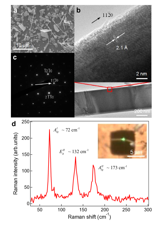
The Bi2Se3 nanoribbons studied here were synthesized via gold catalyzed vapor-liquid-solid mechanism using a horizontal tube furnacePeng10 ; Kong10 . The source material, Bi2Se3 shots (Alfa Aesar, 99.999%), was placed in the center of the hot furnace where the temperature was kept at C during the growth. A Si (100) substrate dispersed with gold catalyst particles ( nm in diameter) was placed downstream at the cold region zone. The tube was flushed with Ar several times before the growth to remove residual oxygen. A 60 sccm Ar flow was kept at 1 Torr at the base pressure of mTorr during the growth. The furnace was cooled down to room temperature after a 1 hour and 30 minute growth. Figure 1a shows a scanning electron microscopy (SEM) image of an as-grown sample. A typical growth usually produces nanoribbons with thickness nm, width nm and length . Figure 1b shows a high resolution transmission electron microscopy (TEM) image from the edge of a typical nanoribbon. The interplanar distance along the nanoribbon growth direction is 0.21 nm, which is consistent with the Bi2Se3 lattice constant ( nm, nm). Figure 1c is a selected area electron diffraction pattern from the same ribbon: all the nanoribbons we have studied so far show a growth direction along . The clear lattice fringes and the electron diffraction pattern indicate that these ribbons are single crystals with little disorder.
We obtained additional confirmation about the crystalline phase of the samples using Raman spectroscopy of individual Bi2Se3 nanoribbons. Figure 1d shows a typical room temperature Raman spectrum from a single Bi2Se3 nanoribbon supported over one of the holes in a TEM grid; the data were taken with 514.5 nm excitation and the geometry ensures that the back scattered light only originates from the nanoribbon of interest. The incident radiation was polarized parallel to the nanoribbon growth direction and the scattered radiation was unpolarized. The measurements were performed with a very low incident laser power (W with a spot size of m) to avoid sample overheating. Three characteristic Raman modes are observed: 72 cm-1, out of plane vibration mode; 132 cm-1, in plane vibration mode; and 173 cm-1, out of plane vibration mode. All these modes are consistent with those observed from bulk Bi2Se3Richter77 .
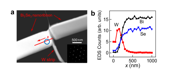
We fabricated electrical transport devices by transferring as-grown Bi2Se3 nanoribbons to a Si substrate with a 1 thick Si3N4 insulating layer and then depositing superconducting tungsten and/or normal platinum (Pt) electrodes using a dual beam focused ion beam (FIB) etching and deposition system. The tungsten contacts are contaminated with carbon and gallium, and consequently have a high superconducting transition temperature (4 K 5 K) and a large critical field ( kOe) Wang_2010 . The correspondingly large superconducting energy gap ( meV) allows good energy resolution in differential conductance measurements. Furthermore, the large critical field lends such devices to explorations of possible vortex formation in regions of proximity-induced superconductivity. The FIB method also has the advantage of forming good ohmic contacts with Bi2Se3 nanoribbons, albeit at the price of localized damage in the contact area. TEM measurements of test structures (Fig. 2a) show that the nanoribbons remain in the single crystal Bi2Se3 phase after FIB deposition, apart from the region immediately underneath the tungsten contacts. The typical electrode is about nm wide and nm high. X-ray energy dispersive profile scans in scanning TEM studies (Fig. 2b) shows that the tungsten spreads about 250 nm from the visible edge of the contact. We conservatively estimate that the contacts have a resistance-area product m2. To rule out the possible shorting between closely spaced tungsten contacts, we also carried out a control measurement by depositing two tungsten strips with a visible edge-to-edge separation of 460 nm on a Si3N4 substrate; we found that the (two-probe) resistance of this configuration was larger than 0.5 M at mK, well below the superconducting transition temperature of the tungsten contacts. To further rule out insidious spreading effects that could occur in a nanostructure geometry, we also examined (undoped) ZnSe nanowires with tungsten contacts and again found no signs of superconducting shorts below the transition temperature of the contacts.
We measured a total of 6 Bi2Se3 nanoribbon devices with tungsten contacts; their characteristics are summarized in Table 1. In addition, we also measured two devices with non-superconducting (Pt) contacts. Although the nanoribbons were all fabricated in the same synthesis run, their dimensions and electrical properties (resistivity) show an inhomogeneous distribution.We are unable to determine the carrier density and carrier mobility because the nanoribbons are too narrow to carry out Hall effect measurements; however, the electrical resistivity of all the devices ( 1 mcm) is of the same order as typical values observed in thin films of Bi2Se3, suggesting similar carrier densities (). We measured the bias-dependent differential conductance in single Bi2Se3 nanoribbon devices using a dc current source and a lock-in amplifier at a frequency of 97 Hz over a temperature range 0.5 K 6 K and in magnetic fields up to 80 kOe. The measurements were performed in both four probe and two probe geometries; the latter measurements are carried out in a “pseudo-four-probe” scheme, with two wires on each contact pad.
III Transport measurements with normal metal (Pt) contacts
Before we discuss transport measurements of Bi2Se3 nanoribbons with superconducting electrodes, we first study transport properties of two devices with non-superconducting electrodes in the four probe geometry. Figures 3a and 3b plot the temperature dependent conductivity for device G and H respectively, showing a variation, consistent with 2D quantum corrections due to weak anti-localization and electron-electron interactionsWang_2011 . Detailed fitting of vs becomes more complicated because of the many fitting parameters: as we show below, fitting the magnetoconductivity to the weak localization theory suggests that there are multiple channels participating in the quantum corrections. Since the slope of vs. is strongly affected by the dependence of , it is not appropriate to assume all channels contribute equally, as this assumes the coherence length for each of the channels is the same as the others. Figures 3c and 3d show the magnetoconductivity for device G and H at K (squares) and K (circles) in fields perpendicular to the nanoribbon plane. We fit the magnetoconductivity using the Hikami-Larkin-NagaokaHLN_1980 equation:
| (1) |
where depends on the dominant scattering mechanism and is the digamma function. in the limit of weak spin orbit and magnetic scattering; in the limit of strong spin orbit scattering and weak magnetic scattering; and when magnetic scattering is strong. For completeness, we also include the 2D correction from electron-electron interactionsLee_1985 given by:
| (2) |
where
| (3) |
and is a function of the average of the static screened Coulomb interaction over the Fermi surface. The solid lines in Figs. 3c and 3d are fits to the above equations, using as fitting parameters the phase breaking length , the parameter and the screening parameter . For device G, the fits yield nm, and at K and nm, and at K. For device H, the fits yield nm, and at K; nm, and at K. Note that the values of the phase breaking length are somewhat smaller than typically seen in thin film samples of Bi2Se3Wang_2011 .
IV Transport measurements with superconducting (tungsten) contacts: observation of a supercurrent and multiple Andreev reflections
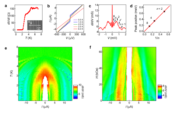
Figure 4a shows the temperature dependence of the two probe zero bias differential resistance () of device A with width nm and thickness nm. The resistance is measured between contacts with edge-to-edge separation (SEM image in the inset). Spreading of the tungsten contacts implies a conservatively estimated Bi2Se3 channel length of nm. The figure shows the onset of the proximity effect at K when the W contacts become superconducting, eventually transitioning to a zero resistance supercurrent state at K. Figure 4b plots the characteristics of this device at different temperatures, showing a critical current A at mK. The product (where is the normal state resistance) has a small value (V ), similar to observations in exfoliated Bi2Se3 layers Sacepe2011 . As expected, decreases with increasing temperature until the supercurrent is completely suppressed at K.
Figure 4c plots vs. at mK, revealing “subharmonic gap structure” due to multiple Andreev reflections at , where is the gap of the W electrodes and is an integer octavio1983 ; Cuevas2006 ; Xiang2006 ; Heersche . The arrows identify a consistent series of subharmonic peaks in corresponding to (Fig. 1d) for a superconducting energy gap meV. Using the BCS relation , this corresponds to K, which is close to K obtained from the temperature dependent zero bias differential resistance. The absence of some values of is not understood, but is not an uncommon occurrence Xiang2006 . The peak assignment in Fig. 4c results in an anomalous location of the prominent peak at 1.194 meV instead of the expected location meV (indicated by the arrow in Fig. 4c). We attribute this to heating at higher bias, noting that similar anomalies have been seen in other SNS devices Xiang2006 . The origin of the peak identified as meV is unclear; it could be a signature of a quasiparticle minigap that is expected to arise when (i.e. when the Thouless energy roughly equals the superconducting gap of the S contacts) Cuevas2006 . The data in Figs. 1a-d provide a clear indication of proximity-induced superconductivity in Bi2Se3. In Figs. 4e and 4f, we map out the detailed variation of as a function of temperature and magnetic field, respectively. These plots show that – as expected from the temperature and field dependence of the superconducting gap of the tungsten electrodes – the multiple Andreev reflection features and are quenched with increasing temperature and field.
Observation of a supercurrent and multiple Andreev reflections in an SNS device requires a normal channel length shorter than two principal length scales: the thermal length which characterizes the spatial decay of the pair amplitude in the N channel and the electron phase-breaking length . At low temperatures, the cut-off is typically determined by . For diffusive channels ( ), , while for ballistic channels ( ), . Here, is the diffusion constant, is the Fermi velocity, is the Boltzmann constant and is temperature. Since we do not directly know the carrier density in our samples, we estimate and based upon some reasonable assumptions. In the normal state, the magnitudes of the resistivity and magnetoresistance of this nanoribbon (cm) are similar to measurements in Bi2Se3 thin filmsRichardella with a carrier density . We thus use this carrier density as an upper limit for and use the Drude model ( ) to yield 50 nm i.e. transport in the channel must be diffusive. Using the experimentally reported effective mass for Bi2Se3, , at roughly this carrier density and for transport normal to the c-axis Hyde_1974 , we estimate a Fermi velocity from and a bulk diffusion constant from . This yields nm at K. We note that even if the assumed nanoribbon carrier concentration was an order of magnitude lower (i.e. ), the corresponding mean free path would be nm and thermal length nm at 1.8 K, both of which are still smaller than the channel length. Next, we estimate a lower bound for by extracting the electron inelastic length from weak antilocalization fits to the magnetoconductance of Bi2Se3 nanoribbons with normal metal (Pt) contacts. (The large for the W contacts precludes a direct measurement of the low temperature magnetoconductance in samples with superconducting contacts.) In the two devices measured (Fig. 3c and 3d), we find nm at K.
Thus, our analysis shows that we are observing a supercurrent and multiple Andreev reflections in SNS junctions with N channel lengths that are significantly longer than the values for and deduced from the diffusive normal state transport. The simplest explanation for this apparent inconsistency is the coexistence of ballistic (surface) and diffusive (bulk) transport channels. We speculate that the latter may dominate the transport in the normal state, but that the proximity-induced superconductivity preferentially occurs in the ballistic surface channel. The validity of this conjecture can be checked by estimating in the ballistic limit, using the value of the Fermi velocity for the TI surface state in Bi2Se3Zhangh09 ; this yields a value nm at K, which is more consistent with the observation of a supercurrent at comparable channel lengths.
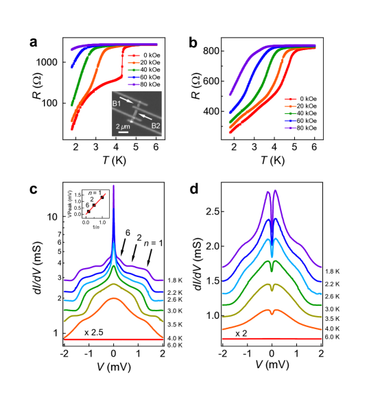
Our hypothesis of a ballistic surface channel that preferentially supports proximity-induced superconductivity is bolstered by transport measurements in three other Bi2Se3 nanoribbon devices. Figure 5 presents data taken on device B, a Bi2Se3 nanoribbon of thickness nm and width nm. The normal state resistivity of this nanoribbon (1.37 mcm) is almost three times greater than device A, yielding shorter estimated elastic and thermal lengths ( 20 nm, 40 nm). This device has two measurable channels (B1 and B2 in the inset to Fig. 5a) with conservatively estimated channel lengths m and m, respectively. Figures 5a-b show the onset of the proximity effect in these channels, while Figs. 5c-d show the bias-dependent differential conductance. The presence of multiple Andreev reflections in channel B1 and their absence in channel B2 are both consistent with our earlier estimate of nm for a clean surface channel since . We have also observed subharmonic gap structure in two additional nanoribbons (not shown). The overall behavior is similar to that discussed above.
V Transport measurements with superconducting (tungsten) contacts: anomalous magnetoresistance oscillations
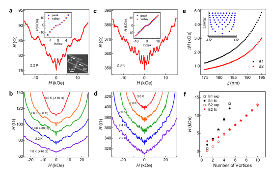
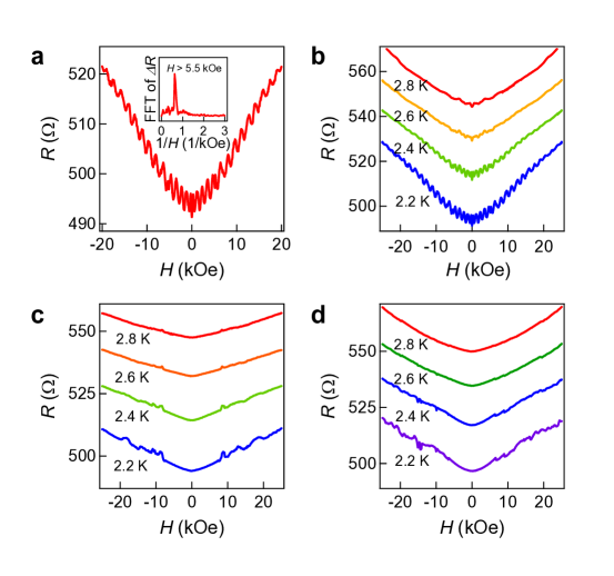
We now discuss the occurrence of unusual MR oscillations in Bi2Se3 nanoribbons under conditions where the contacts become superconducting but where a supercurrent has not yet been established. In order to make consistent comparisons, we carried out both sets of measurements in the two probe geometry on device B, recalling that the electrode configuration shown in Fig. 5a precludes a true four probe measurement for the shorter channel. As a check, we also measured channel B2 in the four probe geometry and found identical behavior as the two probe measurements. Figure 6a shows the MR for channel B1 at = 2.2 K with a magnetic field applied perpendicular to the plane of the nanoribbon. At low field ( kOe), we observe a sharp cusp characteristic of weak anti-localization, similar to earlier results from Bi2Se3nanoribbons contacted with normal electrodes. However, at higher fields, we find well defined and reproducible MR oscillations superimposed on a smooth background. The inset to Fig. 6a plots the magnetic field position of both peaks and valleys. If we exclude the low field region, we find that the MR oscillations are periodic in with a period kOe. Figure 6b shows that the oscillation amplitude varies non-monotonically with temperature, reaching a maximum in the vicinity of = 2.2 K and vanishing at both lower and higher temperatures. Similar behavior is observed in channel B2 except with a smaller period kOe (Figs. 6c and 6d). Similar oscillatory MR has also been observed in 2 other devices. For example, Fig. 7 shows the MR of device D in three primary field orientations: perpendicular to the plane of the nanoribbon (Fig. 7a and 7b), parallel to the nanoribbon axis (Fig. 7c), and parallel to the plane but perpendicular to the axis of the nanoribbon (Fig. 7d). While similar MR oscillations that are periodic ( kOe) at higher field were observed when the field is perpendicular to the nanoribbon plane, they were not observed in the other two primary field directions.
The observed MR oscillations cannot be explained using standard scenarios. The Shubnikov-de Haas effect is ruled out since the oscillations are not periodic in . The Aharonov-Bohm effect of surface currents Peng10 is also ruled out for several reasons: the oscillations are only observed when the magnetic field is perpendicular to the nanoribbon plane and not when it is parallel; the oscillation amplitude has a non-monotonic temperature dependence; finally, MR oscillations are absent when using normal metal contacts (e.g. Pt down to K or W contacts above the superconducting transition temperature), clearly indicating that important role of superconductivity. We note that the Aharonov-Bohm oscillations were not observed in device D in parallel field due to the dominance of the normal transport in a long channel () even when the electrodes are in the superconducting state. We also discount another conventional explanation for the oscillatory MR, namely fluxoid quantization which requires a multiply connected geometry where flux can penetrate normal regions encompassed by a superconductor Sochnikov10 . Assuming fluxoid quantization, the observed oscillation period implies a characteristic geometrical area and for channels B1 and B2, respectively. This is far smaller than any relevant geometrical regions in our devices. The scaling of the oscillation period with the length of the Bi2Se3 channel (B1 and B2), roughly doubling when the channel length is halved, further rules out any insidious fluxoid quantization that might be associated with FIB damage in the contact region.
Having dismissed standard explanations for our observations, we resort to a new model that predicts MR oscillations when a thin, narrow superconducting strip is placed in a perpendicular magnetic field Pekker ; Johansson05 . We are cautiously aware that this “Weber blockade” model was developed for a genuine superconductor, while we are assuming that it can also be applied to a normal metal supporting proximity-induced superconductivity. There is theoretical basis for the formation of vortex-like pair correlations in the N region of diffusive SNS junctions Cuevas_2007 , but we are unaware of a similar prediction for a ballistic case such as the proximity effect in a high mobility TI surface state. In the Weber blockade model, the perpendicular magnetic field controls the number of Pearl vortices in the superconducting strip. Maximum dissipation (i.e. maximum resistance) occurs when the energies of configurations with and vortices are degenerate, and the MR then has a period related to the sequential addition of vortices with increasing magnetic field. Certain observations are immediately consistent with this model: for instance, the onset of periodic oscillations occurs only after a finite field (see insets to Figs. 6a and 6c) and the oscillation period is larger than that expected using fluxoid quantization in the geometric area of the channel. Assuming that a proximity induced superconductor can be described by a uniform superconducting coherence length (distinct from the length scale of the diffusion of Cooper pairs into the superconductor), this model can be extended to predict in the region of proximity induced superconductivity for our geometry.
Using the geometrical parameters for our nanoribbons, we calculated the period of the MR oscillation as a function of the coherence length (i.e. the size of a vortex). Figure 6e shows the result of this calculation for channels B1 and B2, with channel width of 430 nm and nominal channel lengths of 0.94 (squares) and 1.55 (circles), respectively. A comparison with the experimentally observed period yields nm for channel B1 (B2). This length scale corresponds to the size of a vortex in the Bi2Se3 channel and, as expected, is much larger than the coherence length of a typical superconductor (such as the tungsten contacts). The inset to Fig. 6e shows, in a model calculation, how vortices distribute in a nanoribbon as the energy (magnetic field) increases. In Fig. 6f, we plot the number of vortices in the channel as a function of the applied magnetic field, assuming the fitted values of in Fig. 6e. The model assumes a uniform superconducting gap; this may account for the disagreement between the experiment and the calculation using the fitted value of for the first few vortices (Fig. 6f).
VI conclusions
In summary, we have demonstrated proximity-induced superconductivity in Bi2Se3 nanoribbons contacted with superconducting electrodes. Our experiments suggest that even when diffusive bulk conduction coexists with ballistic surface conduction in a 3D TI, the proximity effect may preferentially couple to the latter. Furthermore, the superconductor-TI device configuration demonstrated here provides a viable route for creating vortices near the interface between these two classes of materials. The formation of these vortices is manifest in MR oscillations whose period can be well explained using a simple model. Thus, our experiments show that superconductivity – and possibly vortices – can be realized in experimental geometries that are directly relevant to the search for Majorana fermions in condensed matter systems Fu2008 ; Sau2010 ; Franz2011 .
VII acknowledgement
This work was supported by the Penn State Center for Nanoscale Science under the MRSEC program (NSF grant DMR-0820404). We also acknowledge partial support from ONR. We thank Liang Fu and David Pekker for insightful discussions.
References and Notes
- (1) B. Pannetier and H. Courtois, J. Low Temp. Phys., 118, 599 (2000).
- (2) M. Z. Hasan and C. L. Kane, Rev. Mod. Phys., 82, 3045 (2010).
- (3) X. -L. Qi and S. -C. Zhang, arxiv:1008.2026.
- (4) L. Fu and C. L. Kane, Phys. Rev. Lett. 100, 096407 (2008).
- (5) J. D. Sau, R. M. Lutchyn, S. Tewari, and S. Das Sarma, Phys. Rev. B 82, 094522 (2010).
- (6) A. Cook and M. Franz, arXiv:1105.1787.
- (7) T. D. Stanescu, J. D. Sau, R. M. Lutchyn, and S. Das Sarma, Phys. Rev. B 81, 241310(R) (2010)
- (8) J. Wang, C. -Z. Chang, H. Li, K. He, M. Singh, X. -C. Ma, M. Xie, Q. -K. Xue, and M. H. W. Chan arXiv:1105.6174.
- (9) A. Y. Kasumov, O. V. Kononenko, V. N. Matveev, T. B. Borsenko, V. A. Tulin, E. E. Vdovin, and I. I. Khodos, Phys. Rev. Lett. 77, 3029 (1996).
- (10) L. Fu, C. L. Kane, and E. J. Mele, Phys. Rev. Lett. 98, 106803 (2007).
- (11) D. Hsieh, D. Qian, L. Wray, Y. Xia, Y. S. Hor, R. J. Cava, and M. Z. Hasan, Nature 452, 970 (2008).
- (12) B. Sacepe, J. B. Oostinga, J. Li, A. Ubaldini, N. J. G. Couto, E. Giannini, and A. F. Morpurgo, arXiv:1101.2352.
- (13) Y. S. Hor, A. J. Williams, J. G. Checkelsky, P. Roushan, J. Seo, Q. Xu, H. W. Zandbergen, A. Yazdani, N. P. Ong, and R. J. Cava, Phys. Rev. Lett. 104, 057001 (2010).
- (14) L. A. Wray, S. -Y. Xu, Y. Xia, Y. S. Hor, D. Qian, A. V. Fedorov, H. Lin, A. Bansil, R. J. Cava, and M. Z. Hasan, Nature Phys. 6, 855 (2010).
- (15) D. Pekker, G. Refael, and P. M. Goldbart, arxiv:1010.4799.
- (16) H. L. Peng, K. Lai, D. Kong, S. Meister, Y. Chen, X. -L. Qi, S. -C. Zhang, Z. -X. Shen, and Y. Cui, Nature Mater. 9, 225 (2010).
- (17) D. S. Kong J. C. Randel, H. Peng, J. J. Cha, S. Meister, K. Lai, Y. Chen, Z. -X. Shen, H. C. Manoharan, and Y. Cui, Nano Lett., 10, 329 (2010).
- (18) W. Richter, H. Kohler, and C. R. Becker, Phys. Status Solidi B, 84, 619 (1977).
- (19) J. Wang, M. Singh, M. Tian, N. Kumar, B. Liu, C. Shi, J. K. Jain, N. Samarth, T. E. Mallouk, and M. H. W. Chan, Nature Phys., 6, 389 (2010).
- (20) J. Wang, A. M. DaSilva, C. -Z. Chang, K. He, J. K. Jain, N. Samarth, X. -C. Ma, Q. -K Xue, M. H. W. Chan, Phys. Rev. B, 83, 245438 (2011).
- (21) S. Hikami, A. I. Larkin and Y. Nagaoka, Prog. Theor. Phys. 63, 707 (1980).
- (22) P. A. Lee and T. V. Ramakrishnan, Rev. Mod. Phys., 57, 287 (1985).
- (23) H. Steinberg, J. -B. Laloe, V. Fatemi, J. S. Moodera, P. Jarillo-Herrero, arxiv:1104.1404.
- (24) M. Octavio, M. Tinkham, G. E. Blonder, and T. M. Klapwijk, Phys. Rev. B 27, 6739 (1983).
- (25) J. C. Cuevas, J. Hammer, J. Kopu, J. K. Viljas, and M. Eschrig, Phys. Rev. B 73, 184505 (2006).
- (26) J. Xiang, A. Vidan, M. Tinkham, R. M. Westervelt, and C. M. Lieber, Nature Nanotech. 1, 208 (2006).
- (27) H. B. Heersche, P. Jarillo-Herrero, J. B. Oostinga, L. M. K. Vandersypen, and A. F. Morpurgo, Nature 446, 56 (2007).
- (28) A. Richardella, D. M. Zhang, J. S. Lee, A. Koser, D. W. Rench, A. L. Yeats, B. B. Buckley, D. D. Awschalom, and N. Samarth, App. Phys. Lett. 97, 262104 (2010).
- (29) G. R. Hyde, H. A. Beale, I. L. Spain, and J. A. Woollam, J. Phys. Chem. Solids 35, 1719 (1974).
- (30) H. J. Zhang, C. -X. Liu, X. -L. Qi, X. Dai, Z. Fang, and S. -C. Zhang, Nature Phys. 5, 438 (2009).
- (31) I. Sochnikov, A. Shaulov, Y. Yeshurun, G. Logvenov, and I. Bozovic, Nature Nanotech. 5, 516 (2010).
- (32) A. Johansson, G. Sambandamurthy, D. Shahar, N. Jacobson, and R. Tenne, Phys. Rev. Lett. 95, 116805 (2005).
- (33) J. C. Cuevas and F. S. Bergeret, Phys. Rev. Lett. 99, 217002 (2007).
| Device | Length | Width | Thickness | Contact width | Resistivity at 6 K | Contact material |
|---|---|---|---|---|---|---|
| (m) | (nm) | (nm) | (nm) | (mcm) | ||
| A | 1.08 | 600 | 60 | 200 | 0.51 | W |
| B1 | 0.94 | 430 | 60 | 430 | 1.37 | W |
| B2 | 1.55 | 430 | 60 | 430 | 1.37 | W |
| C | 2.47 | 284 | 276 | 316 | 0.79 | W |
| D | 2.30 | 240 | 77 | 240 | 0.70 | W |
| E | 5.12 | 300 | 98 | 122 | 0.69 | W |
| F | 1.00 | 700 | 60 | 300 | 3.53 | W |
| G | 5.73 | 270 | 60 | 234 | 0.39 | Pt |
| H | 0.94 | 370 | 50 | 280 | 0.48 | Pt |
