Slow conductance relaxation in insulating granular Al: evidence for screening effects
Abstract
It is shown that the conductance relaxations observed in electrical field effect measurements on granular films are the sum of two contributions. One is sensitive to gate voltage changes and gives the already reported anomalous electrical field effect. The other one is independent of the gate voltage history and starts when the films are cooled down to low temperature. Their relative amplitude is strongly thickness dependent which demonstrates the existence of a finite screening length in our insulating films and allows its quantitative estimate (about at ). This metallic-like screening should be taken into account in the electron glass models of disordered insulators.
pacs:
72.80.Ng, 61.20.Lc, 73.23.Hk.During the last 20 years, slow and glassy conductance relaxations were found in several disordered insulating systems FirstExpElectronGlass ; OvadyahuPRB02 ; GrenetEPJB07 . These relaxations have been revealed and often studied by means of field effect measurements. In such experiments, disordered insulating films are used as (weakly) conducting channels of MOSFET devices which allow us to measure their conductance response to gate voltage () changes. After a quench at e.g. , a slow and endless decrease of the conductance is found as long as is kept constant, and any change triggers a new conductance relaxation. Moreover, the system keeps some memory of its history: Any stay under a fixed value remains printed for some time in sweeps as a conductance dip centered on this value. We have also shown recently in granular thin films that these induced relaxations display aging, i.e. the dynamics of the system depends on the time spent at low temperature, a characteristic property of glassy systems GrenetAging10 .
Several experimental findings suggest that these slow conductance relaxations could reflect the properties of the ”electron glass” OvadyahuPRL98 ; OvadyahuElectronGlass , a glassy state theoretically predicted in the 1980s for disordered insulators DaviesPRL82 ; ElectronGlass80 . According to theoretical and numerical studies, a system of electrons with ill-screened interactions and disorder will need an infinite time to reach its equilibrium state at low temperature, the relaxation towards equilibrium being characterized by a conductance decrease of the system RecentEGTheory . Up to now, the electron glass problem has received considerable theoretical developments but only few experimental illustrations, which explain the interest in the electrical field effect results. Moreover, most of the experiments have focused on the electrical conductance and its -induced relaxations but less is known concerning the dielectric properties and their possible time evolution at low .
Since even after a long stay under a fixed the conductance decrease shows no sign of saturation, it is not possible to define the conductance relaxation relative to the equilibrium value, which is unknown. Instead, short excursions to values never explored before are often used to define a history-free reference conductance OvadyahuPRL98 ; OvadyahuPRB02 ; GrenetEPJB07 ; GrenetAging10 . This history-free conductance was sometimes called the ”off-equilibrium” conductance since the system has never been allowed to equilibrate at these s. In the present Letter, we show that is not constant in time after a cool down to in granular films thicker than . We also show that this feature demonstrates the existence of a screening length in our insulating granular films and allows its quantitative estimate.
Our granular films were prepared by e-gun evaporation of under a partial pressure of , as described elsewhere GrenetEPJB07 . By changing the pressure, we can tune the resistance of the films from metallic to insulating. For insulating samples, x-rays and TEM studies have revealed an assembly of crystalline grains with a typical size of a few nanometers. They are believed to be separated by thin insulating layers. MOSFET devices are made by deposition of granular films on top of heavily doped wafers (the gate) covered by a thick thermally grown layer (the gate insulator).
The film conductance was measured by using a two terminal ac technique, employing a FEMTO current amplifier DLPCA 200 and a lock in amplifier SR 7265. Source-drain voltage was such that stays in the Ohmic regime. All the electronic equipments sensitive to room temperature drifts were placed in a thermalized chamber with a stability better than . This last point was crucial in order to follow variations with a precision of during weeks of measurements.
For measurements, the MOSFET devices are mounted in a box filled with He exchange gas and plunged into a liquid He dewar. The sample temperature follows the variations of the liquid He bath around and a carbon glass thermometer close by was used to correct these temperature variations. The time required to cool down the sample from room temperature to is about .
For Fig. 1a, a MOSFET device with a thick granular channel was cooled down to and maintained at this temperature under . Fast sweeps from to ( long) were taken every after the cool down. All the curves display a conductance dip centered on which reflects the memory of the relaxation associated with the stay under . Far enough from (here for ), is roughly constant and this baseline reflects the ”off-equilibrium” conductance previously mentioned. Looking at the time evolution of curves, two features are salient. First, the amplitude of the dip increases as a function of time. This result is well known from previous studies OvadyahuPRL98 ; OvadyahuPRB02 ; GrenetEPJB07 ; GrenetAging10 : the longer the stay under , the more pronounced the dip is. Second, and this is the new feature we aim to discuss here, the baseline conductance also decreases as a function of time. As highlighted in Fig. 1b, the decrease is well described at any s by a dependence, more pronounced in the dip region because of the superposed baseline relaxation and dip growth.
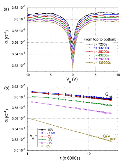
To be more quantitative, we can define a parameter whose physical meaning will become clear later, the slope ratio of the relaxation slope in Fig. 1b at to the relaxation slope (at for example). For the sample of Fig. 1, . We have measured 4 different thick films with values from to . A baseline relaxation was always observed, with at between and . For one film, the gate and the gate insulator were respectively and alumina and consistent results were obtained which excludes any role of a specific gate insulator material. Detailed investigation of the vertical electrical homogeneity of the films has also shown that the baseline relaxation is not related to a specific layer close to the film-substrate interface SupplementaryMaterial .
We checked that this baseline relaxation was independent of the history by using the ”two dip” protocol OvadyahuPRL98 . After some time under , was changed to for the rest of the experiment. We observed the formation of a new dip at and the erasure of the old one at (as already known OvadyahuPRL98 ; GrenetEPJB07 ), but the baseline relaxation in any range far enough from and continue as if no change was imposed.
One may think that the baseline relaxation is induced by the sweeps themselves. Indeed, when measuring curves, a small dip starts to form at each measured point. The baseline thus reflects a short time relaxed value ( being typical for our sweep parameters). We know from the ”two dip” protocol results that a dip formed during will be erased roughly in about OvadyahuPRB02 ; GrenetEPJB07 . In our case, we wait for between two sweeps, thus no memory of the previous sweep is expected out of the dip region. In one experiment, we checked that the baseline relaxation was unaffected by the suspension of sweeps during .
An experimental artifact that may explain the baseline relaxation is the existence of a drift after the cool down. Because of the rapid divergence of the films resistance at low , the observed baseline variations correspond typically to drifts of few ( for the whole relaxation observed at in Fig. 1). We have performed different tests (thermometer stability, comparison with and without exchange gas) which indicate that the drifts are much smaller than the baseline relaxation amplitude. The effect of the film thickness discussed below will definitely ruled out any interpretation in terms of a drift.
If the baseline relaxation is a property of the granular film itself, how can we explain it? A simple hypothesis is to state that the granular film, although electrically insulating, has a metallic-like screening length that is smaller than its thickness ( in Fig. 1). Then, only the layer of the film located at a distance smaller than from the gate insulator is sensitive to changes. The conductance dip reflects the relaxation of this layer, whereas the conductance baseline reflects the relaxation of the rest of the film. The conductance relaxation measured at is then the sum of the two contributions: . Since the relaxations at any are well described by a dependence, we can write and . The slope ratio is by definition equal to . If the film is homogeneous, it is natural to suggest that and are respectively proportional to (the sensitive layer thickness) and (the insensitive layer thickness). Then, as long as . The results for the films ( between 2 and 3) give estimates for the screening length between and .
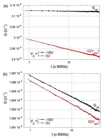
If our simple model is correct, then the baseline relaxation relative to that measured at must change with the thickness of the films. This is illustrated in Fig. 2, where the experiment of Fig. 1 was reproduced for two granular films and thick. A clear thickness dependence is visible. Qualitatively, the baseline relaxation is almost absent for the thick film (Fig. 1a, ) while it is almost equal to that measured at for the thick film (Fig. 1b, ). The agreement with the above simple picture is also quantitative. These values gives estimates of about , close to the results obtained from thick films (). We stress that the variations observed for different thicknesses are much more important than those observed for a given thickness and different .
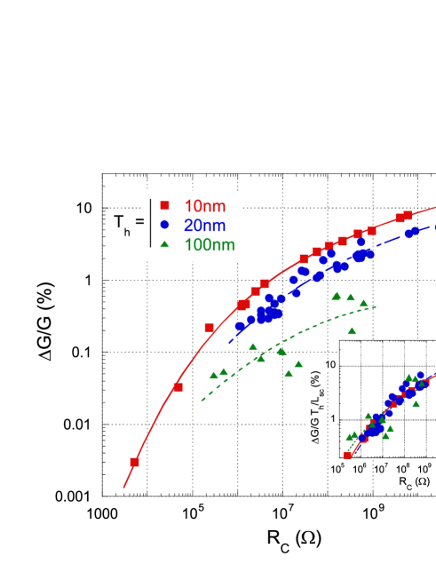
Our simple model also predicts a thickness dependence for the amplitude of the conductance dip . data, measured for , and thick films are shown in Fig. 3 as a function of their percolation critical resistance ESBook84 . In 2D films ( less than the percolation radius ), , but for thicker ones, . Taking DelahayeEPJB08 , we estimate as for and films and for films. All the samples were measured after being kept under for after a cool down at . As can be seen and was already reported FirstExpElectronGlass ; GrenetEPJB07 , increases significantly with . Besides, a clear reduction of is visible for a given as increases, in qualitative agreement with the fact that the conductance dip originates from a layer of a fixed thickness. The agreement is also quantitative. As long as , does not depend on . Let us note its value (of course depends on ). When , one has (). Then, plotting for all the samples should give one single curve . This is confirmed in the inset in Fig. 3 for which we have assumed a screening length of for all the films.
Finally, our model provides a natural explanation for the increase of the data scatter with the thickness, as observed in Fig. 3. Small variations of the pressure or of the evaporation rate are always present during the deposition of granular films. Thus in thick samples, the measured (and the estimated ) does not necessarily reflect the resistance of the unscreened thick layer deposited on top of the gate insulator which determines the amplitude of the dip. The quality of the scaling in the inset in Fig. 3 is indeed an indirect test of the vertical homogeneity of the films, as discussed in details in Ref. SupplementaryMaterial .
We now come to a discussion of our results. First, note that the thickness dependence of clearly demonstrates that the conductance relaxation exists in the ”bulk”” of the film and is a property of the granular itself (and not of its interface with the gate or the surface oxide layer). The ”bulk” relaxation after a cool down at is well described by a dependence without any sign of saturation over weeks of measurement. Such a dependence was also observed for the time increase of the conductance dip amplitude after a cool down OvadyahuPRB02 ; GrenetEPJB07 (more complex laws are observed when is fixed a time after the cool down, see GrenetAging10 ). It is a natural relaxation law for a system having a distribution of relaxation times, as expected for an electron glass AmirRecent .
In our granular thin films, the electronic transport at finite is believed to result from electron tunneling between metallic grains. A lower bound for is then the typical grain size, which was found in recent TEM measurements to be . A second important microscopic length scale is the percolation radius of the critical resistance network. Since in our films , the diffusion of charge carriers through the critical resistance network is expected to be faster than the time scale of the measurements (the intergrain capacitance and the capacitance of the granular channel to the gate are respectively and ). Thus, should be an upper bound for as indeed observed: estimates from conductance fluctuations measurements are between and DelahayeEPJB08 , a few times our value.
We note that no baseline relaxation was reported on thick indium oxide films which may indicate that in this system. Interestingly enough, was found to be in ”crystalline” films OrylanchikPRB07 , i.e. times our estimate for granular films, reflecting a less dense percolating network in indium oxide consistent with a larger screening length.
Our observations address the important question of screening in a disordered insulator, a subject which has been little explored both theoretically and experimentally. Electron glass models are generally developed in the limit of strongly localized electrons DaviesPRL82 ; ElectronGlass80 ; RecentEGTheory (Ref. VignalePRB87 ; Dobrosavljevic are exceptions). But in real systems, there is a mobility of the charge carriers at finite which will give rise to a metallic-like screening. Numerical studies on disordered insulators have indeed found a transition between a metallic screening at high where most of the electrons are diffusive and a slow dielectric response at low where most of the electrons remain located in finite size clusters XuePRL88 ; DiazPRB99 ; KoltonPRB05 . Such a transition was observed around in capacitive measurements on a doped semiconductor DonMonroePRL87 . According to the usual formula, , where is the thermodynamic DOS. In a glassy phase and for a finite time , the system cannot explore all the configurations and the thermodynamic DOS has to be replaced by a pseudo-equilibrium DOS for which only relaxations faster than are allowed. The first theoretical attempts to do so DaviesPRL82 ; MullerPRB07 have found that the short time ( Maxwell time) screening length diverges as goes to 0 and decreases as a function of time MullerPRB07 .
In summary, we have described in insulating granular films the existence of a insensitive conductance relaxation. Its thickness dependence demonstrates the existence of a metallic screening length of about at . Our results provide a new way to study the screening length and its relaxation in disordered insulators where an anomalous electrical field effect has been found. They also point to the need for more theoretical studies: how are the classical electron glass models predictions affected by the existence of a metallic screening length ?
This research has been partly supported by the French-National Research Agency ANR (contract ).
References
- (1) M. Ben-Chorin et al., Phys. Rev. B 44, 3420 (1991); G. Martinez-Arizala et al., Phys. Rev. Lett. 78, 1130 (1997); T. Grenet, Eur. Phys. J. B 32, 275 (2003).
- (2) A. Vaknin et al., Phys. Rev. B 65, 134208 (2002).
- (3) T. Grenet et al., Eur. Phys. J. B 56, 183 (2007).
- (4) T. Grenet et al., to be published in Eur. Phys. J. B.
- (5) A. Vaknin et al., Phys. Rev. Lett. 81, 669 (1998).
- (6) Z. Ovadyahu, Phys. Rev. Lett. 99, 226603 (2007); Z. Ovadyahu, Phys. Rev. B 78, 195120 (2008); Z. Ovadyahu, Phys. Rev. Lett. 102, 206601 (2009).
- (7) J. H. Davies et al., Phys. Rev. Lett. 49, 758 (1982).
- (8) M. Grünewald et al., J. Phys. C 15, L1153 (1982); M. Pollak and M. Ortuño, Sol. Energy Mater. 8, 81 (1982).
- (9) For recent Ref., see C.C. Yu, Phys. Rev. Lett. 82, 4074 (1999); D.N. Tsigankov et al., Phys. Rev. B 68 184205 (2003). M. Müller and L. Ioffe, Phys. Rev. Lett. 93, 256403 (2004); V. Malik and D. Kumar, Phys. Rev. B 69, 153103 (2004); D.R. Grempel, Europhys. Lett. 66, 854 (2004); E. Lebanon and M. Müller, Phys. Rev. B 72, 174202 (2005); A.M. Samoza et al., Phys. Rev. Lett. 101, 056601 (2008).
- (10) See EPAPS Document for a discussion of the vertical electrical homogeneity of the granular films.
- (11) B.I. Shklovskii and A.L. Efros, Electronic Properties of Doped Semiconductors (Springer-Verlag, New York 1984).
- (12) J. Delahaye et al., Eur. Phys. J. B 65, 5 (2008). The existence of a screening length was not taken into account in this Ref. and the values reported for films must be divided by a factor .
- (13) A. Amir et al., Phys. Rev. B 77, 165207 (2008); A. Amir et al., Phys. Rev. Lett. 103, 126403 (2009).
- (14) V. Orlyanchik and Z. Ovadyahu Phys. Rev. B 75, 174205 (2007).
- (15) G. Vignale, Phys. Rev. B 36, 8192 (1987).
- (16) A.A. Pastor and V. Dobrosavljević, Phys. Rev. Lett. 83, 4642 (1999); V. Dobrosavljević et al., Phys. Rev. Lett. 90, 016402 (2003).
- (17) W. Xue and P.A. Lee, Phys. Rev. B 38, 9093 (1988).
- (18) A.B. Kolton et al., Phys. Rev. B 71, 024206 (2005).
- (19) A. Díaz-Sánchez et al., Phys. Rev. B 59, 910 (1999).
- (20) Don Monroe et al., Phys. Rev. Lett. 59, 1148 (1987).
- (21) M. Müller and S. Pankov, Phys. Rev. B 75, 144201 (2007).