Tunable thermal conductivity in defect engineered nanowires at low temperatures
Abstract
We measure the thermal conductivity () of individual InAs nanowires (NWs), and find that it is 3 orders of magnitude smaller than the bulk value in the temperature range of 10 to 50 K. We argue that the low arises from the strong localization of phonons in the random superlattice of twin-defects oriented perpendicular to the axis of the NW. We observe significant electronic contribution arising from the surface accumulation layer which gives rise to tunability of with the application of electrostatic gate and magnetic field. Our devices and measurements of at different carrier concentrations and magnetic field without introducing structural defects, offer a means to study new aspects of nanoscale thermal transport.
pacs:
Thermal transport measurements on semiconducting nanowires (NWs) have attracted a lot of attention in the last few years. Measurements of thermal transport in nanostructures are important as they provide a platform to test the existing descriptions of phonons in confined structures and across complex interfaces complexthermoreview , and have the potential to result in technological applications as thermoelectric systems complexthermoreview ; cahillreviewJAP ; cahillreviewJHT . Different materials are benchmarked using the thermoelectric figure of merit , where is the Seebeck coefficient, is the electrical resistivity, is the thermal conductivity and is the absolute temperature. can be increased by appropriate engineering of nanostructures. One of the ways to increase is by reducing without degrading its electrical conductivity and Seebeck coefficient hicks . As a result, an ideal thermoelectric material is a glass for phonons and ordered for electronic transport. Recently, several theoretical models as well as experimental studies have been carried out in different semiconductor NWs like Si, Ge, Bi2Te3 etc. deyu ; mingo2 ; renkun ; hochbaum ; jimheathsinanowire . It is found that for Si NWs, the value of is reduced by two orders of magnitude deyu ; hochbaum ; jimheathsinanowire compared to bulk values by tuning the roughness of the surface. III-V semiconductors are also known to be good thermoelectric materials, and theoretical studies suggest that InSb and InAs NWs are good candidates for better mingo1 . InAs NWs have been studied extensively to probe their charge and spin-transport inas-spin-orbit-samuelson ; our-inas ; newpaper . An aspect of InAs NWs that makes studying their thermal transport, hitherto little explored persson ; shiinasnw , of interest is the ability to tune the density of twin defects and polytypes along its length by varying growth parameters twin-hiruma ; xiong ; caroffp ; InP ; petta-inas . Exploiting this control over crystal structure can help synthesize defect-engineered NWs, whose lattice has aperiodic array of twins along its length that modify phonon behavior, without significantly compromising their electrical properties petta-inas . Such NWs satisfy the key criteria for a good thermoelectric material – localization of phonons without localizing electrons.
In this work we explore the of suspended InAs NW field effect transistors (FETs); the NWs have high density of aperiodic twins and polytypes perpendicular to their axis twin-hiruma ; xiong ; caroffp ; petta-inas . The random nature of defects suppresses (the phonon contribution to ) resulting in reduction of thermal conductivity by 3 orders of magnitude from bulk. Our method also has an advantage which is to study as a function of carrier concentration without introducing additional impurities. We observe significant change in the thermal conductivity with the application of gate voltage suggesting finite electronic contribution, and we propose that this contribution comes from the conduction electrons at the surface accumulation layer which is inherent to low band gap semiconductors like InAs and InN petrovykh ; Tilburg ; thickness . To confirm the role of electronic contribution we apply magnetic field and see considerable changes in the thermal conductivity.
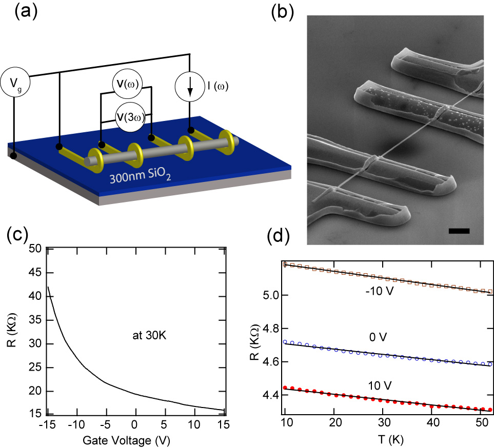
The InAs NWs used to fabricate the devices in this work were grown in a metal organic chemical vapour deposition (MOCVD) system using the vapor-liquid-solid (VLS) technique on a oriented GaAs substrate. NWs of 100 - 200 nm diameter were used in this experiment. 10-12 m long NWs were chosen for making four probe suspended devices on a nm thick, SiO2 coated degenerately doped Si wafer, which serves as the back gate (growth and device fabrication details are given in supplementary S1 supp ). Fig. 1(a) shows the schematic of the device and the circuit for electrical and thermal measurements. Fig. 1(b) shows a scanning electron microscope (SEM) image of a device. The gold electrodes provide mechanical support and Ohmic contacts with negligible contact resistance to the suspended NW besides thermally anchoring it at four points to the bath temperature Tb. The electrical properties of the device are characterized as a function of gate voltage (Vg) and temperature before detailed thermal transport measurements. Fig. 1(c) shows the resistance (R=) of a typical device as a function of Vg at a fixed value of Tb. The n-type field effect transistor (FET) behavior of the suspended NW devices is clearly seen. Fig. 1(d) shows the evolution of R as a function of temperature, T, and also the corresponding linear fit in the temperature range 10-50 K.
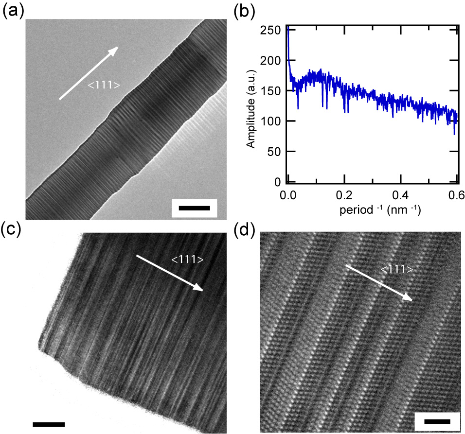
High resolution transmission electron microscopy (TEM) studies were used to characterize the microstructure of our twin-engineered NWs. Fig. 2(a) shows a large scale TEM image of a NW where we observe an aperiodic arrangement of the twin superlattice perpendicular to its axis. The fact that the lattice has defects but lacks a long-range periodicity is reflected in the Fourier amplitude (seen in Fig. 2(b)) that has no sharp peaks along the length of the NW. Figs. 2(c) & (d) show a detailed view of the twins and polytypes twin-hiruma ; xiong ; caroffp ; petta-inas . The typical spacing of these defects is 3-5 nm. Once electrical and structural characterization is done, we perform simultaneous thermal and electrical measurements.
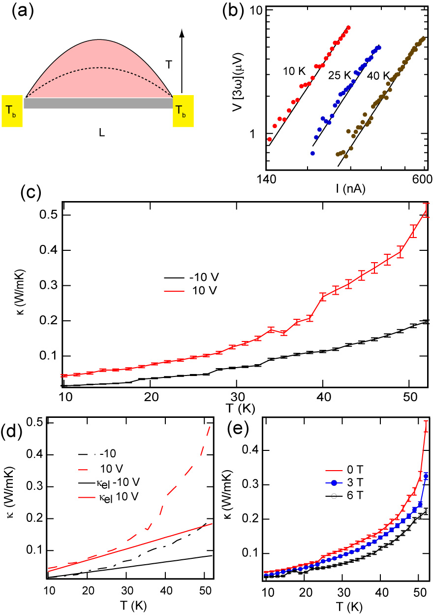
One method of measuring thermal properties of nanostructures uses a modification of the 3 technique cahill3omega for and specific heat measurement. The modified 3 technique 3omega ; dames3omega ; nickelnanowire relies on fabricating suspended four probe devices with the conducting NW serving both as a heater and a thermometer. The magnitude of V() can be related to (in the limit ) as 3omega ; dames3omega
| (1) |
where is the angular frequency of the AC current, is its amplitude, and are the resistance and the derivative of resistance with respect to temperature respectively, is the length of the NW between the two middle probes and , its cross section. 3omega ; dames3omega . For our devices, is m and the thermal time constant can be estimated to be s (details of phase information of signal in the limit of are given in the supplementary S2 supp ).
To measure at each temperature value, we vary the current (I) and obtain from the fitting of Equation 1 to the measured V as a function of injected I. Fig. 3(b) shows the evolution of V with I along with the cubic power-law relationship that is essential to ensure that the technique is applicable within the applied current regime (to eliminate other source that can possibly show cubic scaling see supplementary S4 supp ). As we vary the temperature, we also record the resistance. We determine from the derivative to the linear fit to the plot (see Fig. 1(d)). The variation of with becomes small and non-monotonic above 50-60 K this is the reason we choose the temperature range of 10-50 K in our experiment. The phase of the signal is measured to be zero at all temperatures (see supplementary Fig. S2 supp ). This procedure of fitting the power law given by Equation 1 at each instance of parameter space allows us to extract as a function of Vg and temperature. We have calibrated our technique using lithographically fabricated 170 nm wide 75 nm thick gold NWs in the temperature range of our measurement and obtained a Lorenz number around (see supplementary S3 supp ) which calibrates the measurement technique we have used.
Fig. 3(c) shows the plot of measured as a function of temperature at two values of Vg. The overall magnitude of is about 1000 times smaller than the bulk values inasbulkkappa (see supplementary Fig. S14 supp ). This is a significant reduction in and the measured value is similar to the minimum thermal conductivity model of Cahill et al. cahill-minimumthermal (CWP model) based on the assumption that the material is highly disordered. Similar reduction in , beyond the CWP model, was also observed in disordered WSe2 which is a layered structure wse2 . Later we return to a model to understand this better. Similar evolution of is also observed at different values of Vg in all the measured devices (see supplementary Fig. S 10-12 supp ).
Now we consider the effect of Vg on . It is clear that the electrical conductance of the semiconducting NW FET can be modified as a function of Vg (Fig. 1(c)). However, the effect of electron density variation is not expected to affect in most semiconducting materials, as phonons are the dominant carriers of heat zimanbook . Direct calculation from electrical conductivity using the Wiedemann-Franz (WF) law gives a small value of the electronic contribution () which does not explain the variation we see with Vg (see supplementary S6 supp ). To understand the origin of large we have to first understand the material property of the InAs wire. It is well known that in InAs there is an accumulation of charge at the surface. The resultant downward band bending pins the surface Fermi level above the conduction band minimum petrovykh ; thickness ; Tilburg . In a geometry where the surface to volume ratio is large, such as NWs, this surface accumulation charge (SAC) plays a major role in the electrical transport. The SAC takes part in the electrical conduction and scatters due to roughness at surface, which is also the reason for low electron mobility in InAs NWs compared to bulk our-inas ; Tilburg . We have passivated our devices using (NH4)Sx but this passivation leads to further enhancement to the surface charge density ( petrovykh and consequently excellent Ohmic contacts. Fig. 1(c) shows that our device is always in conducting state throughout the gate range with low resistance value, strongly suggesting the presence of the accumulation layer. To estimate the we have to consider the thickness of the layer of this SAC since it will reduce the effective cross sectional area through which heat is transported by electrons. The electrons in the bulk and in the accumulation layer can be thought of two parallel channels conducting heat and we can define a effective layer thickness () to find out the actual from the WF law,
| (2) |
where and are length and radius of the wire respectively, R is the electrical resistance at temperature and is Lorenz number. We can get a rough estimate of from above equation by assuming that at lowest temperature the phonon contribution () is small and . For the NW of length 2.6 m and radius 70 nm we get from our data as 20 nm and 10 nm for applied gate voltages of -10V and +10V respectively. Now we use Equation 2 to find for all , the result is plotted as solid lines in Fig. 3(d). This estimated from a simplified picture captures the variation we see in our data with . Another confirmation about this non negligible comes from our magnetic field measurement. One way to suppress the electronic contribution is to apply a magnetic field zimanbook ; royal , as it will reduce the electronic mean free path for heat transport by deflecting the semiclassical trajectory of electrons. We have done measurement in magnetic field up to 6T and see considerable reduction of thermal conductivity (see in Fig. 3(e)). Magnetic field can affect phonons via electron-phonon interaction, the amount of change in however, is much smaller elph than the effect we see in our measurement.
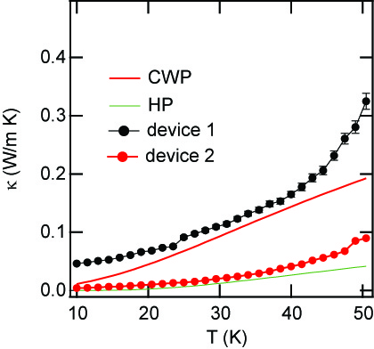
The total is small and it is important to understand the origin of reduction in . It is clear from the structural analysis in Fig. 2 that our NWs have a high density of twins. The twin defects introduce additional interfaces and also cause the surface to be rough, with typical roughness 2-3 nm. The heat conduction in bulk is dominated by phonons whose mean free path is much larger than the spacing between defect planes throughout the temperature range of our measurements (see supplementary Fig. S16 supp ). The average number of defect interfaces is 500 per m – this makes the problem challenging to model comprehensively. However, previous experiments on ordered superlattice-venky ; hurley-superlattice , quasiperiodic superlattices hurley-aperiodic and calculations with modulation of superlattice mahan-minimumthermalconductivity ; ren-superlattice on similar lengthscale suggest that suppression of takes place in such structures. Our devices have aperiodic interfaces (see Fig. 2(a)) and they are likely to attenuate a wide band of phonons. Additionally, modeling indicates that heat transport across grain boundaries can offer significant thermal impedance maiti-acrossgrainboundaries . In order to understand the magnitude of the observed , we use a model by Hopkins et al. minimumkappainterface (denoted by HP model) which explicitly takes into account the role of interfaces for calculating minimum in layered materials. We have calculated the predicted values of the model of Cahill et al. cahill-minimumthermal (denoted by CWP model) and the HP model for InAs (see supplementary S9 supp ). There is a range of measured for devices made from different NW samples (see supplementary S5 supp ); data from two such devices at 0 Vg is shown in Fig. 4. Without introducing any free parameters, the predictions of the CWP and HP models result in values that are comparable to the range in measured in our experiments.
In summary, we demonstrate that thermal conductivity of InAs NWs with twin defects and polytypes is 1000 times smaller than bulk values which will make our devices suitable candidates for good thermoelectric materials. We show the electronic contribution becoming significant due to presence of the surface charge accumulation. The ability to tune thermal conductivity electrostatically can lead to novel ways of probing heat transport in defect engineered nanostructures, and possible device applications.
We would like to acknowledge the Government of India for support (TIFR grant numbers 11P803, 11P809 and 11P812).
References
- (1) G. J. Snyder & E. S. Toberer Nat Mater 7, 105–114 (2008).
- (2) D. G. Cahill et al. J. Appl. Phys 93, 793–818 (2003).
- (3) D. G. Cahill, K. Goodson & A. Majumdar J. Heat Trans. 124, 223–241 (2002).
- (4) L. D. Hicks, M. S. Dresselhaus Phys. Rev. B 47, 12727–12731 (1993).
- (5) L. Deyu et al. Appl. Phys. Lett. 83, 2934–2936 (2003).
- (6) N. Mingo, L. Yang, D. Li & A. Majumdar Nano Lett. 3, 1713–1716 (2003).
- (7) R. Chen et al. Phys. Rev. Lett. 101, 105501 (2008).
- (8) A. I. Hochbaum et al. Nature 451, 163–167 (2008).
- (9) A. I. Boukai et al. Nature 451, 168–171 (2008).
- (10) N. Mingo Appl. Phys. Lett. 84, 2652–2654 (2004).
- (11) C. Fasth et al. Phys. Rev. Lett. 98, 266801 (2007).
- (12) S. Dhara et al. Phys. Rev. B 79, 121311 (2009).
- (13) S. Nadj-Perge et al. Nature 468, 1084-1087 (2010).
- (14) A. I. Persson et al. Nano Lett. 9, 4484–4488 (2009).
- (15) A. Mavrokefalos et al. In Thermoelectrics, 2006. ICT ’06. 25th International Conference on, 234–237 (2006).
- (16) K. Hiruma et al. J. Appl. Phys. 77, 447–462 (1995).
- (17) Q. Xiong, J. Wang & P. C. Eklund Nano Lett. 6, 2736–2742 (2006).
- (18) P. Caroff et al. Nat Nano 4, 50–55 (2009).
- (19) R. E. Algra et al. Nature 456, 369–372 (2008).
- (20) M. D. Schroer & J. R. Petta Nano Lett. 10, 1618-1622 (2009).
- (21) D. Y. Petrovykh, M. J. Yang, L. J. Whitman Surface Science 523, 231–240 (2003).
- (22) J. W. W van Tilburg et al. Semicond. Sci. Technol. 25, 024011 (2010).
- (23) S. A Dayeh, E. T Yu, D. Wang Small 5, 77-81 (2009).
- (24) See supplementary material at [http://www.tifr.res.in/ nano/] for details.
- (25) D. G. Cahill Rev. Sci. Instrum. 61, 802–808 (1990).
- (26) L. Lu, W. Yi & D. L. Zhang Rev. Sci. Instrum. 72, 2996–3003 (2001).
- (27) C. Dames & G. Chen Rev. Sci. Instrum. 76, 124902–124914 (2005).
- (28) M. N. Ou et al. Appl. Phys. Lett. 92, 063101–063103 (2008).
- (29) P. V. Tamarin & S. S. Shalyt Sov. Phys. Semicond. 5, 1097–1098 (1971).
- (30) D. G. Cahill, S. K. Watson & R. O. Pohl Phys. Rev. B 46, 6131 (1992).
- (31) C. Chiritescu et al. Science 315, 351–353 (2007).
- (32) J. M. Ziman Electrons and phonons: the theory of transport phenomena in solids (Oxford University Press, Oxford, 1960).
- (33) K. Mendelssohn, H. M. Rosenberg P. Roy. Soc. Lond. A MAT. 218, 190-205 (1953).
- (34) J. P. Eisenstein, A. C. Gossard, V. Narayanamurti Phys. Rev. Lett. 59, 1341–1344 (1987).
- (35) V. Narayanamurti et al. Phys. Rev. Lett. 43, 2012 (1979).
- (36) D. C. Hurley et al. Phys. Rev. Lett. 58, 2446 (1987).
- (37) D. C. Hurley et al. Phys. Rev. B 37, 8829 (1988).
- (38) M. V. Simkin & G. D. Mahan Phys. Rev. Lett. 84, 927 (2000).
- (39) S. Y. Ren & J. D. Dow Phys. Rev. B 25, 3750 (1982).
- (40) A. Maiti, G. D. Mahan & S. T. Pantelides Sol. St. Comm. 102, 517–521 (1997).
- (41) P. E. Hopkins & E. S. Piekos Appl. Phys. Lett. 94, 181901–181903 (2009).