Solid phase epitaxy amorphous silicon regrowth : some insight from empirical molecular dynamics simulation
Abstract
The modelling of interface migration and the associated diffusion mechanisms at the nanoscale level is a challenging issue. For many technological applications ranging from nanoelectronic devices to solar cells, more knowledge of the mechanisms governing the migration of the silicon amorphous/crystalline interface and dopant diffusion during solid phase epitaxy is needed. In this work, silicon recrystallisation in the framework of solid phase epitaxy and the influence on orientation effects have been investigated at the atomic level using empirical molecular dynamics simulations. The morphology and the migration process of the interface has been observed to be highly dependent on the original inter-facial atomic structure. The interface migration is a quasi-planar ideal process whereas the cases and are much more complex with a more diffuse interface. For , the interface migration corresponds to the formation and dissolution of nanofacets whereas for a defective based bilayer reordering is the dominant re-growth process. The study of the interface velocity migration in the ideal case of defect free re-growth reveals no difference between and and a decrease by a mean factor of 1.43 for the case . Finally, the influence of boron atoms in the amorphous part on the interface migration velocity is also investigated in the case of orientation.
pacs:
68.55.A-Nucleation and growth and 81.15.AaTheory and models of film growth1 Introduction
Advanced technological research work dedicated to silicon materials process engineering needs to control the silicon recrystallisation process at the nanometer scale for nanoelectronic Duffy07 ; Saenger07 or photo-voltaic devices Agaiby ; Huet09 . The silicon film re-growth occurs during annealing when amorphous regions or layers are created by parasitic phenomena like in vapor-liquid-solid (VLS) grown silicon nanowires or intentionally, to limit diffusion effects like in advanced junction depth processing Duffy04 . However, it is really difficult to reach a deeper understanding of the many effects taking place during regrowth. For example, the rich interplay between the nucleation rate, the interface roughening, the defects generation or dissolution and the dopant diffusion is difficult to characterise by using only experimental fabrication and characterisation techniques.
From the theoretical point of view, there is a debate on the general physical description of crystal growth Chernov04 . The concept of a localised interface approach where the nucleation and growth process take place was first introduced by Burton, Cabrera and Frank BCF51 . On the other hand, the concept of a diffuse interface where an ordering flux is associated to the interface migration is also proposed. This flux is assumed to be generated by the counterbalance between the atomic forces interaction induced by the short-range order and the thermal motion Chernov04 . In this framework, solid phase regrowth is often described as an thermal activated process shown by the following equation :
| (1) |
where T is the interface temperature, v0 is the exponential prefactor and Ea is the activation energy. For silicon phase epitaxy, the debate focused on the nature of defects (dangling bonds, kink sites, vacancies, interstitials) on their location (crystal, interface, amorphous part) and on their influence on the limited growth rate Aziz91 . The influence of interface orientation, stress or dopant is also under debate. Atomistic process modelling Pelaz09 in the framework of molecular dynamics is expected to help to clarify the physical picture. This method could probably provide more insight into the re-growth mechanisms taking place at the amorphous/crystalline interface during thermal annealing. Dopant incorporation and the associated diffusion effects during re-growth are much more complex to simulate compared to the bulk case Cuny06 . Moreover, information technology achieved significant progress and enabled the simulation of relatively large atomic configurations that could match experimental systems.
Preliminary simulation studies of the silicon solid phase epitaxy related to junction processing by molecular dynamics were performed by Mootoka et al. Motooka00 . But many open questions remain on solid phase epitaxy like the substrate orientation influence despite clear technological interest. More knowledge is available in the case of melt-interfaces re-growth Grabow89 . This problem has also been investigated using a finite elements based method or lattice Kinetic Monte Carlo (KMC) Bragado09 but numerous challenges are faced to take into account the complex reordering processes at the atomic level. The main objective of this paper is to present the work performed in order to investigate the influence of orientation and dopant effects on the amorphous silicon re-growth mechanisms. The first section briefly describes the computational details and the method used in this work. Some complementary tests related to the influence of the initial properties of the disordered layer are also provided. In a second part, most important results concerning the influence of the interface orientation on recrystallisation mechanisms are presented and discussed. Preliminary results on the influence of Boron atoms on the interface migration velocity are also provided. Finally, some important conclusions are drawn in the last section.
2 Methods
2.1 Computational details
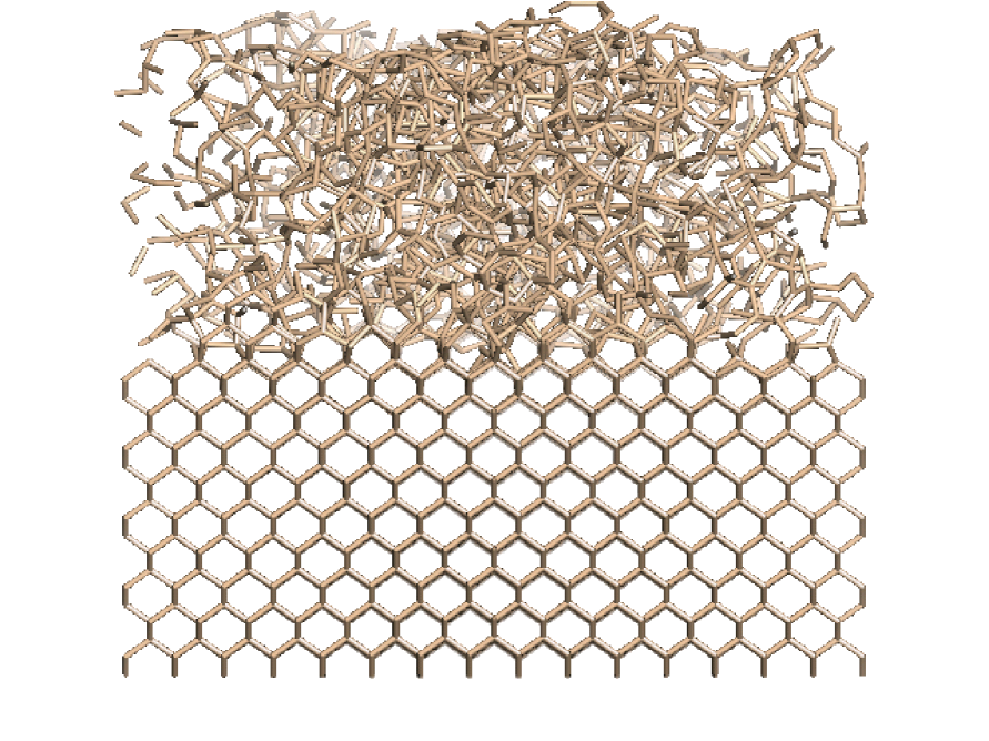
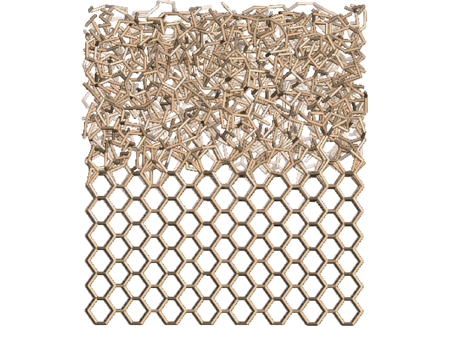
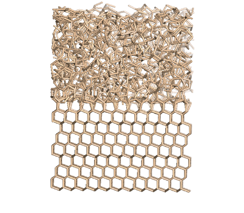
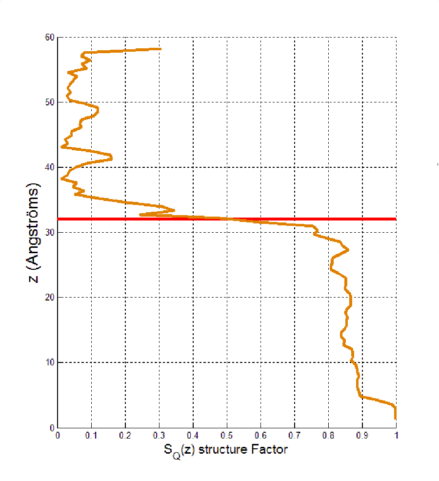
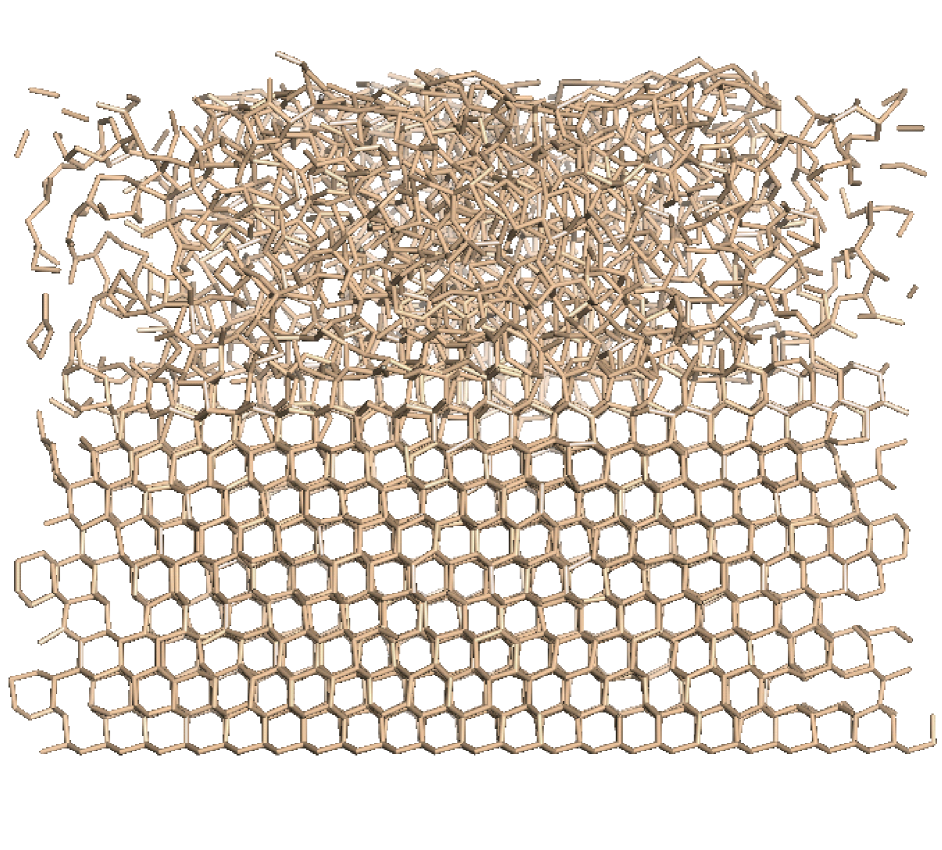
Empirical molecular dynamic simulations have been undertaken in this work in order : i) to generate the amorphous and ii) to simulate the annealing step and the recrystallisation of an amorphous/crystalline silicon interface. In order to generate the disordered part, a melting process simulated by a thermal annealing at high temperature with a low quenching rate Ishimaru97 is considered. The procedure has been repeated for the three clusters built along directions , and and containing respectively 4928, 5120 and 5184 atoms. The cell size parameters (8 8 10) is a trade-off between reasonable computational costs and a possible influence of the periodic conditions on regrowth rate. Fig 1 illustrates the various initial configurations. In order to simulate the layer re-growth, the Molecular Dynamics (MD) technique can also be applied to estimate the various atomic displacements at a given temperature in the framework of a Nosé-Hoover thermostat Nose-Hoover . The two most used empirical potentials Tersoff Tersoff and Stillinger-Weber (SW) SW are under study in this work. The regrowth velocity determination is based on the evolution of the -Si/-Si or -Si interface. This location is estimated by using a plane structure factor as a function of the depth Mattoni04 as shown in Fig. 2. The temperature range for annealing is a function of the empirical potential and is given in Table 1. Only lateral periodic boundary conditions are considered leaving the possibility to the stack to expand or contract. In order to perform a uniform doping in the amorphous part, a specific approach has been developed. The amorphous part is sliced in various trenches of different thicknesses. Boron atoms are introduced in the amorphous lattice in a substitutional way. After the dopants introduction, the equilibration of the cluster is performed by a short annealing step leading to a final dopants distribution located in the amorphous part. Different concentration levels of boron are considered from the lowest one (0.2%) up to (5.4-6%). In the case of Molecular Dynamics with doped boron systems, only the Tersoff potential has been used. It is often claimed that no empirical potential describes properly the subtle Si-B and B-B interactions. In this work, the approach of Pérez-Martín et al. Perez_Martin04 is followed where boron atoms are assumed to adopt a similar behaviour in silicon like carbon atoms.
2.2 Recrystallisation velocity and disordered part properties
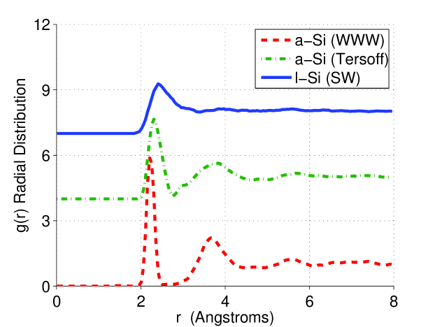
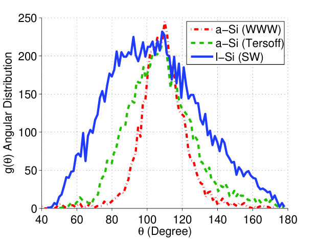
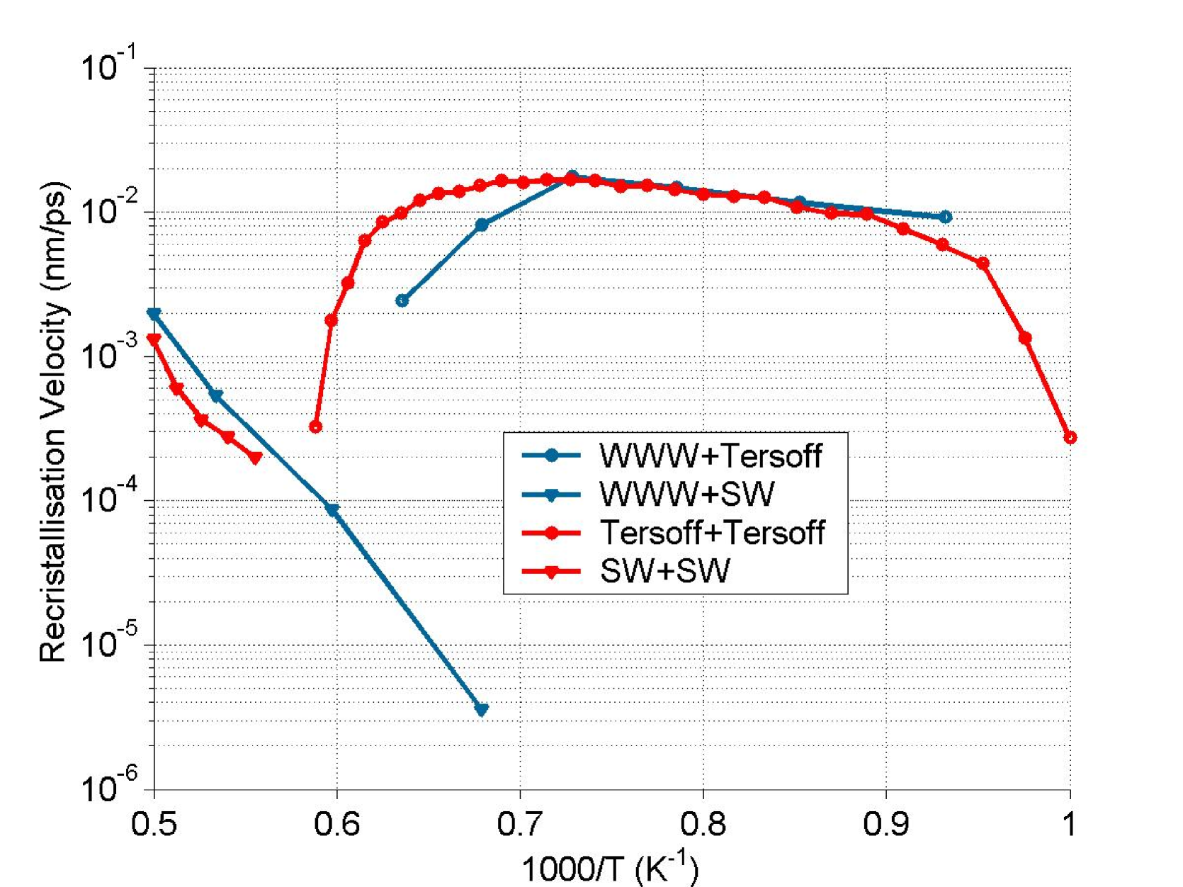
In a previous work, it has been shown that for the simulation of silicon solid phase epitaxy the empirical potential must be taken carefully into account with the high sensitivity to describe or preserve an amorphous structure during annealing Krzeminski07 . However, there is a debate on the influence of the initial properties of the disordered part and the recrystallisation velocity obtained by molecular dynamics. In this work, the quality of the initial interface has been enhanced in comparison to previous studies where only a Wooten Winer Weaire’s amorphous cluster on a crystalline box was considered. The two main usual methods for generating a virtual amorphous cluster (Monte-Carlo bond switching Wooten85 or by melting-quench) are confronted. The melting temperature used to generate a liquid part and next the quenching rate is described in Table 1. As shown in Fig. 3 and also in table 2, large differences for the different properties (from radial and angular distribution to the mean coordination number distribution) in the disordered part can be observed. Fig. 4 reports the recrystallisation velocity of the -Si or -Si/-Si interface for the two main potentials Tersoff and Stillinger-Weber (SW). For the recrystallisation velocity obtained using a Tersoff potential, Arrhenius kinetics have been observed for the two different amorphous in relative close agreement characterised with the same activation energy of 2.9 eV. The situation is completely different in the case of a simulated annealing using Stillinger-Weber. Despite the fact that in the first case, an initial -Si/-Si structure whereas in the second case a completely different -Si/-Si interface is under consideration, small differences can be observed. Clear liquid phase epitaxy characteristics with velocity re-growth of about a few m/s in a wide temperature range limited by the melting of the crystalline part is observed slightly above a temperature of 1675K. These results strengthen our previous conclusions about the major influence of the empirical potential used for the estimation of the recrystallisation velocity and on the variability of empirical potentials to preserve an amorphous structure upon annealing Krzeminski07 .
3 Results and discussion
3.1 Orientation effects and solid phase epitaxy
3.1.1 Regrowth mechanisms
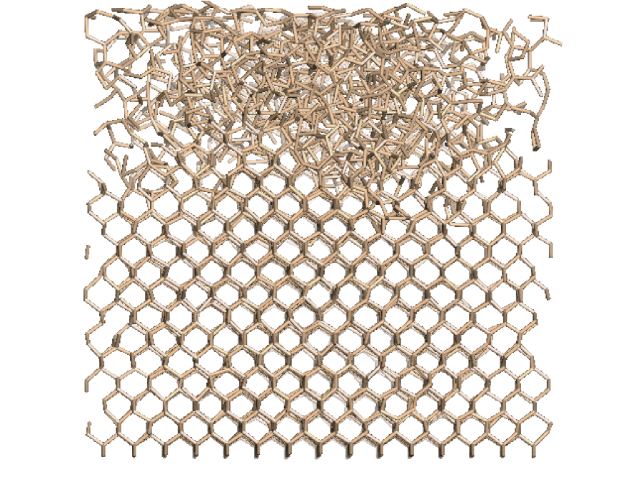
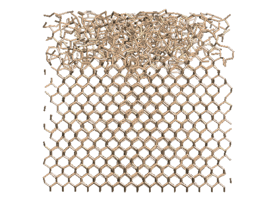
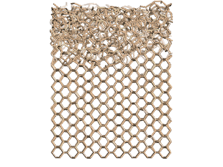
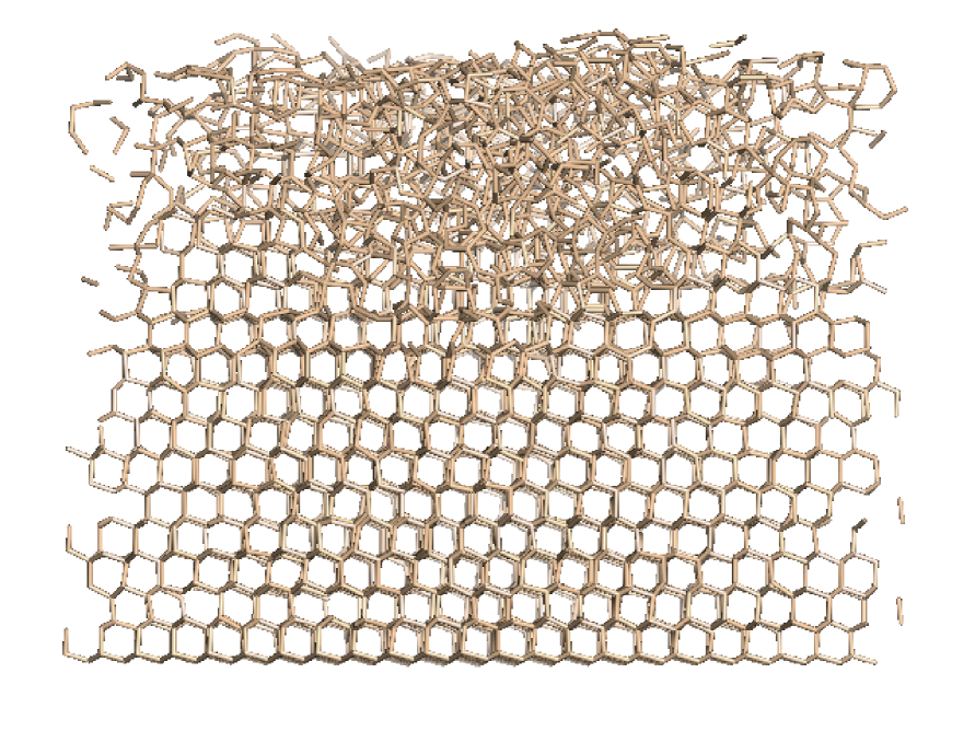
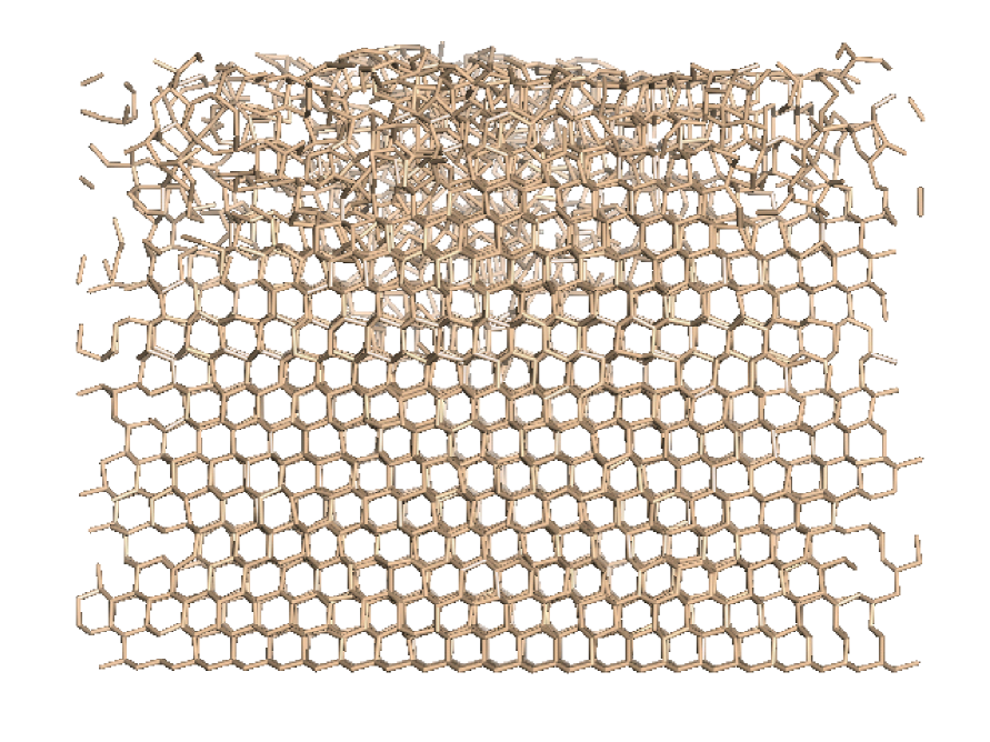
The influence of the interface orientation effect on the re-growth mechanism has been investigated. The interface migration process is studied for the different crystalline orientations , and . Fig. 5 presents the -Si/-Si for an interface migration at 1700K during thermal annealing. For , the re-growth front is governed by first a diffusion process in the disordered part, then by a partial ordering at the interface and finally by a one-by-one atom incorporation. The propagation of the crystalline front proceeds in a quasi-planar -Si/-Si interface with some partial reordering which could extend to one or two planes.
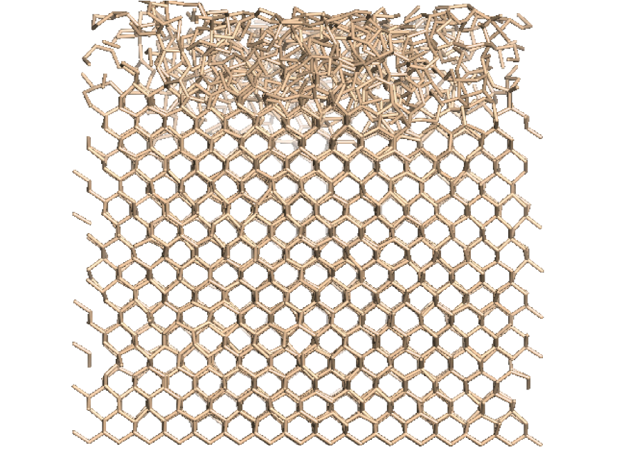
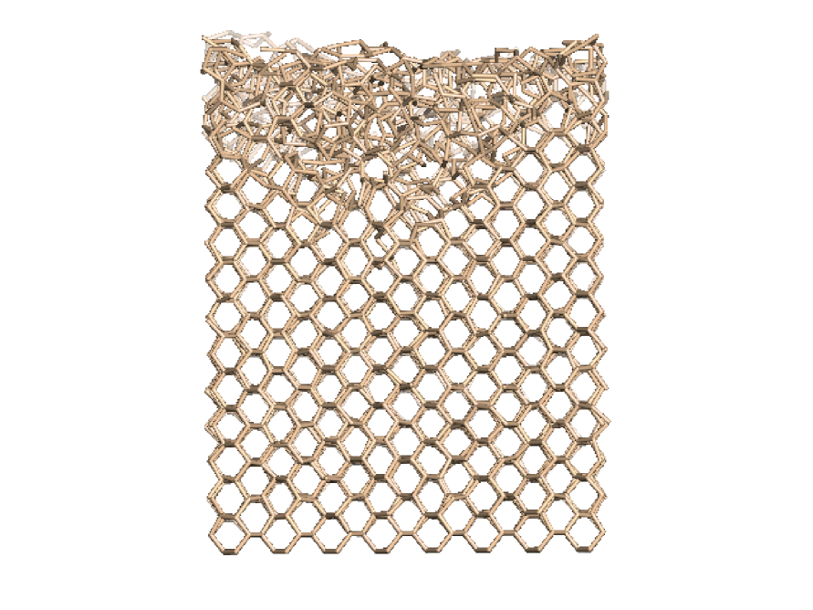
For the orientation a relative different mechanism has been observed in Fig. 6. Two silicon atoms have to be incorporated at the recrystallisation front and then to bind with each other. In order to get a second atom and to complete the crystalline plane, the recrystallisation is observed to propagate also vertically in another nucleation site. The re-growth front predicted by simulation is made of nanofacets leading to the formation of a sawtooth interface of about 3-4 atomic planes. For , the interface is more diffuse and characterised by a more important roughness as a partial ordering extend to several atomic planes.
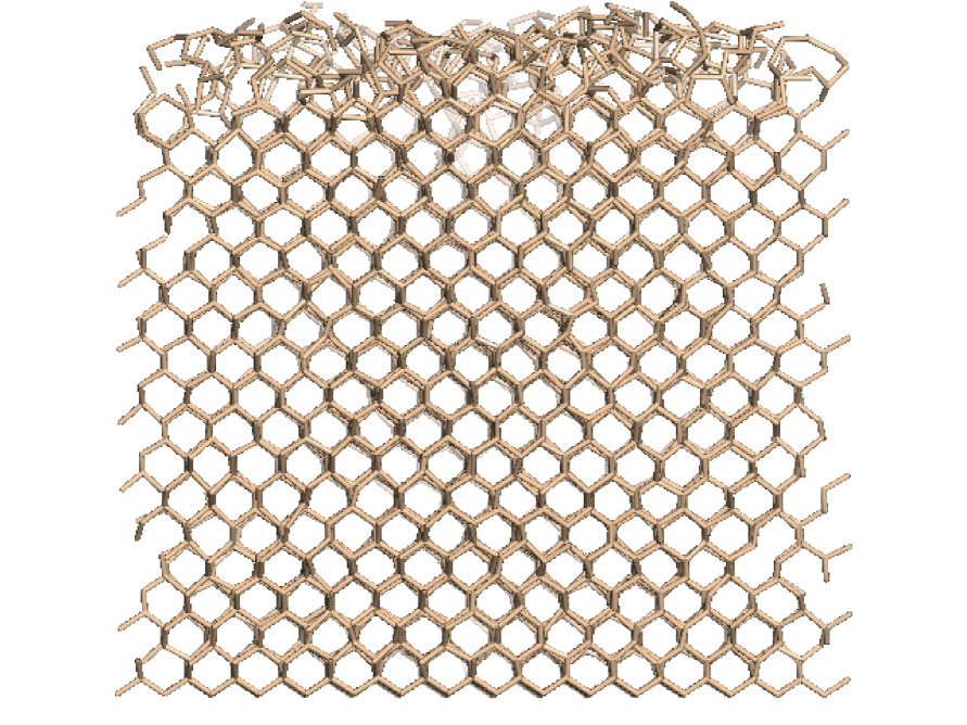
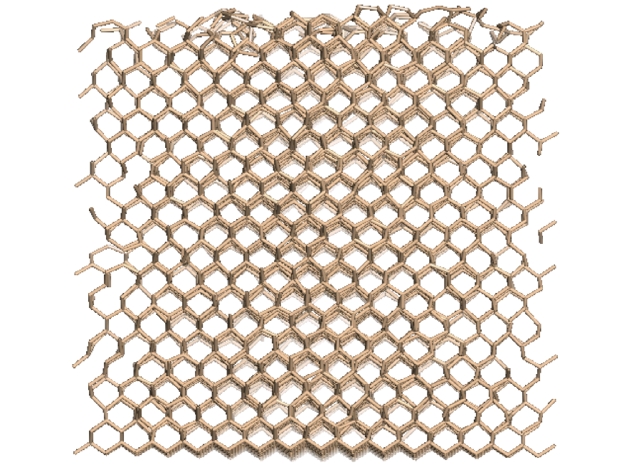
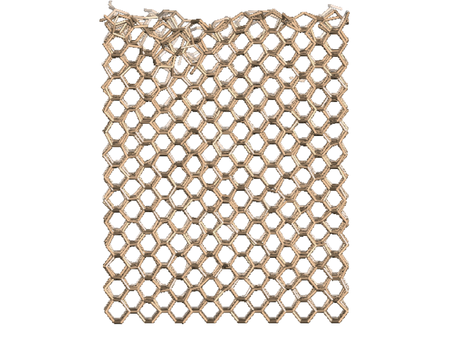
For the case , the recrystallisation mechanisms are observed to be even more complex (Fig. 7) in comparison with and . The migration from -Si to -Si occurs by the rearrangements of complete or partial bilayers. For example, in the case of Fig. 7 incomplete bilayers form on the right and left part, while the central part is slowly rearranging (10 ns and 20 ns) letting suddenly appear several crystalline layers (25 ns). A buried defect at the top surface remains. The interface migration is made of successive plateaus whose height correspond to the distance (or a multiple of the distance) between the bilayers . The formation of one or more twins in planes has been observed in nearly all the temperatures simulated. Other defects are observed in about 50 % of the simulations. The interface recrystallisation interface is also completely different and mostly based on a bilayer process. For , the silicon atoms tends to organise partially in bilayer with a significant time necessary for the atomic arrangements within the the bilayer as three atoms of the bilayer are involved in the atomic process for the creation of a six-fold rings. Again, in the case , the recrystallisation process is not strictly planar with a large interplay between in and out of plane nucleation.
3.1.2 Orientation dependent recrystallisation velocity
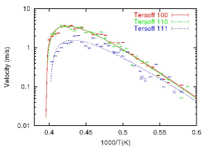
One main open question concerns the influence of the re-growth mechanisms related to orientation effects at the -Si/-Si interface. Fig. 8 presents an example of the interface velocity extraction in the intrinsic case for the three orientations under study. This corresponds to the case where it was possible to define an -Si/-Si interface using a planar structure factor. This is not possible for in-plane and extended defects which generate too much disorder to allow a proper interface definition. All the systems considered are free from defects except for systems containing only twin parallel defects. In this particular case, the orientation is estimated to be kept since it is only a default in the stacking plane sequence. The results as a function of the temperature and for the three orientations are given in Fig. 8 in the temperature range that could be considered with a reasonable computing time. It can be observed that while being very close in the orientations and , the velocity is lower along the direction by a factor 1.43. For the orientation , the activation energy can be extracted using the classical theory of thermally activated growth Lu91 . Considering the fact that the interface velocity reported in the Arrhenius plot is superimposed or either parallel, there was no reason to consider a different activation energy for the cases and .
3.2 Discussion
The theoretical picture given by molecular dynamics simulations stresses the importance of the initial interface orientation on the growth mechanisms. It has been observed that solid phase epitaxy mechanisms are strongly dependent on the interface orientation with a quasi-planar migration for the interface. This propagation is compatible with most analytical modelling based on a sharp interface migration. For and , the situation is relatively different with the formation respectively of nanofacets for and a bilayer mechanism leading to the formation and the migration of a more complex and diffuse interface associated with the generation of defects. Even if the physical reality described by molecular dynamics is more complex, some connections could be made with the phenomenological model of Drosd and Washbrun Drosd82 which described the initial recrystallisation steps Lampin09 . The results on the interface recrystallisation velocity are more complicated to confront with experimental results. One main issue in our study is to define an interface migration velocity in the case where the -Si/-Si interface is more diffuse and characterised by the presence of defects. In this paper, only free-defect re-growth is considered. It corresponds to an ideal physical picture which is not observed experimentally Drosd82 . The resulting activation energy of the process for the various orientation is 2.87 eV in accordance with the experimental range of [2.4-2.9]eV Drosd82 ; Olson88 ; Csepregi78 . This activation energy cannot be associated with a simple active process like self-diffusion or defects migration. This energy seems rather associated with the energy barrier at the interface as suggested by Posselt et al. Posselt09 . Since some bond breaking and exchange between the amorphous and the silicon phase and exchange are often observed in our simulation in order to allow a proper definition and propagation of the -Si/-Si interface. Some links could be made with the picture given by molecular dynamics and the approach of Lu et al. Lu91 which considered the dangling bond breaking, moving and trapping mechanism as the main process responsible for the growth rate limitation Aziz91 . The prefactor for orientation (1.2107 m/s) is reduced by a factor 1.43 compared to and suggesting that the atomic incorporation mechanism based on three atoms at interface [111] slows down the overall interface migration compared to the other orientation. Only a small part of the velocity reduction can be explained by our molecular dynamics simulation. Since experimentally more interface recrystallisation velocity reduction is observed for and , the role and the influence of defects on the nucleation velocity should be investigated more in depth at the theoretical level. A remaining open question that should be addressed concerns the influence of the cell size particularly in a large presence of defects. It seems to be the most plausible hypothesis to explain the reduction velocity effects.
3.3 Regrowth of a doped -Si:B/-Si interface
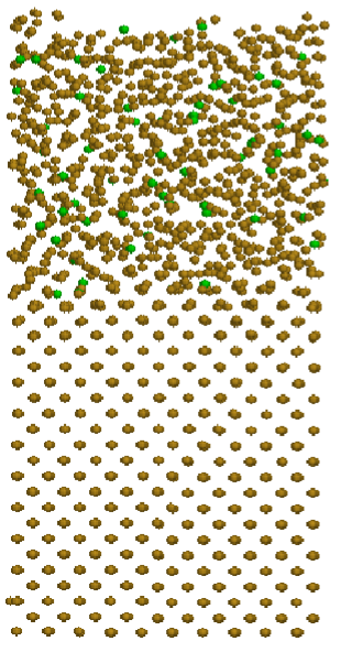
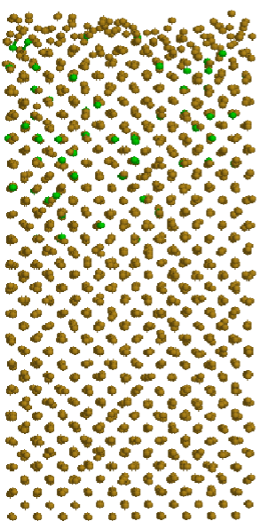
The possible influence of boron atoms in the silicon amorphous part has been investigated in the case of interface . The implantation step has not been Fig. 9 presents an example of initial doped -Si (doped)/-Si interface and illustrates the final state where the amorphous part is completely recrystallised with most of the boron atoms incorporated in substitutional positions of the crystalline matrix. This result is in agreement with a previous study on the annealing of damage generated by octodecaborane implantation Marques06 . The results concerning the interface recrystallisation velocity are first detailed just below and then discussed in further subsection.
3.3.1 Interface recrystallisation velocity
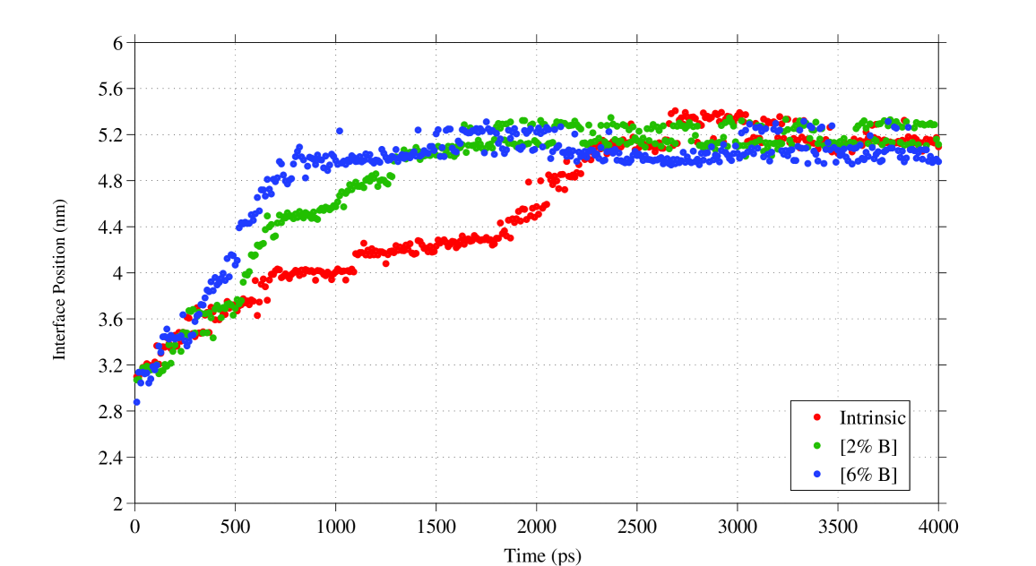
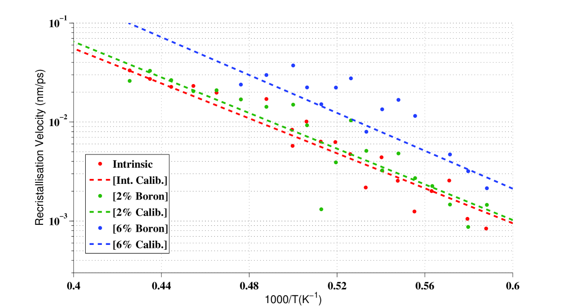
Fig. 10 reports the evolution of the interface position at 2000K 111which would correspond to a rescaled temperature of about 1000∘C for different boron concentrations. In this case, it is clearly shown that the presence of boron is increasing the velocity of the interface migration. Fig. 11 summarises all the computer experiments performed in the intrinsic case and for 2 % and 6 % boron concentration configurations. Basically, for most temperatures, it can be observed that there is no significant difference between the intrinsic case and the 2 % case. The calibration by an Arrhenius law for the last case gives the same activation energy and a small difference for the prefactor (6.2 %). For a very large boron concentration (6 %), a small increase in the solid phase epitaxy velocity is observed leading to an increase in the prefactor by a ratio 1.34.
3.3.2 Discussion
In this work, a complete different behaviour has been observed compared to similar previous molecular dynamics simulations performed by Mattoni et al. Mattoni03 . Using molecular dynamics in the framework of the Stillinger-Weber empirical potential, an increase of the re-growth velocity at low boron concentrations (below 1%) has been observed whereas for larger concentrations (1% up to 10%) the velocity is reduced. On the experimental side Olson88 , it has been observed that below 0.06 %, the boron concentration has almost no influence on the recrystallisation velocity. However, around 0.2 %, a significant increase is observed up to a factor 10 at a low temperature annealing (C). Our results obtained using Tersoff are much more in agreement with the experimental picture and the observed minor influence of boron at low concentration. Probably, in the case of Stillinger-Weber simulation, the mechanism is more compatible with a framework of liquid phase epitaxy with the high tendency of SW based -Si for melting even at low temperature Krzeminski07 . Compared to the experimental results, it would not be so surprising that the influence of dopant is largely underestimated by our empirical molecular dynamics simulation since the Fermi level variations in our system are not taken into account theoretically. Generalised Fermi-Level Shifting (GFLS) model and the influence of charged defects at the interface are often assumed empirically with some success to estimate the enhancement of the normalised re-growth rate defined by the ratio of the doped recrystallisation velocity in the doped with the intrinsic one Johnson08 :
| (2) |
where Ef and Ed are respectively the Fermi level and the defect level in the band gap whereas is the degeneracy factor. As pointed out by Johnson et al. Johnson08 more work is needed in this direction in order to confirm the validity of the GFLS approach. First, a more refined description level which incorporates electronic structure and Fermi shift such as tight-binding or ab-initio molecular dynamics would probably be mandatory for such a purpose. Next, the ideal system under study (doped -Si:B/-Si interface) has probably to be improved in order to match the experimental picture since for example dopant implantation is known to generate large amounts of defects (end of range defects, interstitials ,…) and surface roughness.
.
4 Conclusions
Empirical molecular dynamics simulation have been undertaken in order to investigate the silicon re-growth at the atomic level. Earlier results on the influence of the empirical potential and the large sensibility of the virtual silicon amorphous to the atomic force description have been again illustrated. On the other hand, it has been observed that the interface migration velocity estimated is not so sensitive to the way a virtual amorphous silicon cluster is generated provided the amorphous character is preserved during annealing. The influence of orientation effects has been investigated at the atomic level showing a large influence of the surface orientation effects on the recrystallisation mechanism. The physical picture described by molecular dynamics is more complex than the classical re-growth theory since the relation between the atomistic structure of the interface and the defects generation is clearly underlined. The concept of a sharp interface often used in the classical theory must be put in perspective as molecular dynamics suggests a more diffuse interface. More attention is probably needed to investigate more in depth the influence of defect on velocity re-growth. Concerning doping effects, a small increase in the recrystallisation velocity has been observed at large doping concentration. Further work is clearly needed in this direction to study if the influence of charged defects could be introduced empirically in molecular dynamics simulation in order to validate or not the generalised Fermi-level shifting model often assumed by the classical re-growth theory.
Acknowledgements.
The authors are grateful to Jean-Michel Droulez for his regular support on information technology aspects and to Fabrizio Cleri for stimulating discussion on molecular dynamics. This work has been supported partly by the European Commission as a contribution to the project PULLNANO under contract n∘ IST-026828 from the Information Society Technologies Programme (IST).References
- (1) R. Duffy, M. J. H. Van Dal, B. J. Pawlak, M. Kaiser, R. G. R Weemaes, B. Degroote, E. Kunnen, E. Altamirano, Appl. Phys. Lett., 90, 241912, (2007).
- (2) K. L. Saenger, J. P. de Souza, K. E. Fogel, J. A. Ott, C. Y. Sung, D. K. Sadana, H. Yin, J. Appl. Phys., 101, 024908, (2007).
- (3) R. M. B. Agaiby, M. Becker, S. B. Thapa, U. Urmoneit, A. Berger, A. Gawlik, G. Sarau and S. H. Christiansen, J. App. Phys., 107, 3319654, (2010).
- (4) S. Huet, P. Juliet, X. Ducros, F. Sanchette, United States Patent, 7592198 B2, (2009).
- (5) R. Duffy, V. C. Venezia, A. Henriga, B. J. Pawlak, M. J. P. Hopstaken, G. C. J. Maas, Y. Tamminga, T. Dao, F. Roozeboom and L. Pelaz, Appl. Phys. Lett., 84, 4283 (2004).
- (6) A. A. Chernov, J. Cryst Growth, Vol. 264, Issue 4, p. 499-518, (2004).
- (7) W. K. Burton, N. Cabrera, F. C. Frank, Phil. Trans. R. Soc. Lond. A, Vol. 243, 866, p. 299-358, (1951).
- (8) Guo-Quan Lu and Eric Nygren and Michael J. Aziz, J. Appl. Phys., Vol. 70, 5323, (1991).
- (9) L. Pelaz, L. A Marqués, M. Aboy, P. López and I. Santos, J. Eur. Phys. B, 72, 323 (2009).
- (10) V. Cuny, Q. Brulin, E. Lampin, E. Lecat, C. Krzeminski and F. Cleri, Europhys. Lett., 76, 842, (2006).
- (11) T. Motooka, K. Nisihira, S. Munetoh, K. Moriguchi, A. Shintani, Phys. Rev. B, 61, 8537, (2000).
- (12) M. H. Grabow, G. H. Gilmer and A. F. Bakker, in Atomic Scale Calculations in Materials Science, edited by J. Tersoff, D. Vanderbilt, and V. Vitek, Mater. Res. Soc. Symp. Proc., Vol. 141, Pittsburgh, (1989).
- (13) I. Martin-Bragado and V. Moroz, Appl. Phys. Lett., 95, 123123, (2009).
- (14) M. Ishimaru, S. Munetoh, T. Motooka, Phys. Rev. B, 56, 15133, (1997).
- (15) S. Nosé, Molec. Phys.52, 255 (1984). W. G. Hoover, Phys. Rev. A 31, 1695 (1985).
- (16) J. Tersoff, Phys. Rev. B 38, 9902 (1988).
- (17) F. H. Stillinger and T. A. Weber, Phys. Rev. B 31, 5262 (1985).
- (18) A. Mattoni and L. Colombo, Phys. Rev. B, 69, 045204, (2004).
- (19) A. Mari Carmen Pérez-Martín, José J. Jiménez-Rodriguez, José Carlos Jiménez-Sáez, Applied Surface Science, 234, 228, (2004).
- (20) C. Krzeminski, Q. Brulin, V. Cuny, E. Lecat, E. Lampin, F. Cleri, J. Appl. Phys., 101, 2743089 (2007).
- (21) F. Wooten, K. Winer and D. Weaire, Phys. Rev. Lett. 54, 1392 (1985).
- (22) R. Drosd, J. Washburn, J. Appl. Phys., 53, 1982.
- (23) E. Lampin and C. Krzeminski, J. Appl. Phys., 106, 063519 (2009).
- (24) G. L. Olson and J. A. Roth, Mater. Sci. Rep. 3, 1 (1988).
- (25) Csepregi, E. F. Kennedy, J. W. Mayer, T. W. Sigmon, J. Appl. Phys.,49, (1978).
- (26) M. Posselt and A. Gabriel, Phys. Rev. B, 80, 045202, (2009).
- (27) G.-Q. Lu, E. Nygren and M. J Aziz, J. Appl. Phys., 70, 5323, (1991).
- (28) L. A. Marqués, L. Pelaz, I. Santos and V. C. Venezia, Phys. Rev. B, 74, 201201(R), (2006).
- (29) A. Mattoni and L. Colombo, EPL (Europhysics Letters), 62, 6, (2003).
- (30) B. C. Johnson, P. Gortmaker, J. C. McCallum, Phys. Rev. B, 77, 214109, (2008).
| Potential | Annealing Range (K) | Melting (K) | Quenching Rate (K/ps) |
|---|---|---|---|
| Tersoff | [1700-2500] | 3500 | |
| SW (Standard) | [1000-1700] | 2200 |
| Conditions | CN | 2fold | 3fold | 4fold | 5fold | 6fold |
|---|---|---|---|---|---|---|
| -Si, WWW | 3.63 | 7.6 % | 19.7% | 70.8 % | 0.9% | 0% |
| -Si, Tersoff | 4.17 | 0.7 % | 9.9% | 63.4 % | 24 % | 1.9 % |
| -Si, SW | 2.92 | 24. % | 38.5% | 25.67% | 3.4 | 0.16 % |
