Surface Scattering via Bulk Continuum States in the 3D Topological Insulator Bi2Se3
Abstract
We have performed scanning tunneling microscopy and differential tunneling conductance () mapping for the surface of the three dimensional topological insulator Bi2Se3. The fast Fourier transformation applied to the image shows an electron interference pattern near Dirac node despite the general belief that the backscattering is well suppressed in the bulk energy gap region. The comparison of the present experimental result with theoretical surface and bulk band structures shows that the electron interference occurs through the scattering between the surface states near the Dirac node and the bulk continuum states.
pacs:
73.20.-r, 72.20.Dp, 72.25.-b
Recent discovery of topological insulators has aroused great attention to the new state of quantum matter originating from the surface state that forms a massless Dirac cone centered at time-reversal invariant momentum Kane_PRL_05 ; Bernevig_PRL_06 ; Bernevig_Science_06 ; Konig_Science_07 ; Hsieh_Nature_08 ; Hsieh_Science_08 ; Xia_NatPhys_09 ; Chen_Science_09 ; Kuroda_PRL_10 ; Fu_PRB_07 ; Zhang_NatPhys_09 ; Hsieh_Nature_09 . Unlike the spin-degenerate Dirac fermions in graphene, this novel electronic state possesses helical spin textures protected by time-reversal symmetry, which creates the potential for spintronics devices without heat dissipation and for quantum computation applications. The topological insulator phase has been predicted to exist in a number of three-dimensional materials, Bi1-xSbx Fu_PRB_07 , Bi2Se3, Bi2Te3, and Sb2Te3 Zhang_NatPhys_09 . The spin-helical surface states have been experimentally observed by angle-resolved photoelectron spectroscopy (ARPES) Hsieh_Nature_08 ; Xia_NatPhys_09 ; Chen_Science_09 ; Kuroda_PRL_10 , also with spin resolution Hsieh_Science_08 ; Hsieh_Nature_09 ; Nishide_PRB_10 .
Among the binary chalcogenides, Bi2Se3 is regarded as the most promising candidate owing to the single ideal Dirac cone residing in a wide band gap (0.3 eV). Therefore, significant effort has been applied towards the realization of spintronics devices using the quantum topological transport in Bi2Se3 Checkelsky_PRL_09 ; Analytis_PRB_10 ; Eto_PRB_10 ; Butch_PRB_10 . The magnetotransport measurements showed Shubnikov-de Haas oscillations originating from the 3D Fermi surface, but no surface contribution to conduction has been observed in 3D topological insulators even at low carrier density Analytis_PRB_10 ; Eto_PRB_10 ; Butch_PRB_10 .
These observations pose the question of what limits the surface electron conduction in Bi2Se3. Band structure calculations of Ref. Xia_NatPhys_09 predict the Dirac point of the surface state in Bi2Se3 to be located below or close to the bulk valence band maximum, which may open a scattering channel from the surface states to bulk continuum states Xia_NatPhys_09 . In this Letter, we present scanning tunneling microscopy evidence of the near-surface scattering of the spin polarized surface states at the Dirac point in Bi2Se3 into spin-degenerate bulk continuum states.
The scanning tunneling microscopy (STM) and spectroscopy (STS) experiments were conducted at 78K and at 4.5K in an ultrahigh vacuum with a base pressure of 110-10 mbar using a low-temperature scanning tunneling microscope (LT-STM, Omicron NanoTechnology). The STM images were acquired in the constant-current mode with a bias voltage applied to the sample. The images were obtained simultaneously by recording the STM images using a lock-in technique. Bi2Se3 samples were cleaved in situ at room temperature in an ultrahigh vacuum to minimize the surface contamination. For comparison, a photoemission spectrum was measured with a hemispherical photoelectron analyzer (VG-SCIENTA R4000) at Hiroshima Synchrotron Radiation Center, Hiroshima University. The crystal structure of Bi2Se3 consists of weakly bonded 5-layer (quintuple layer) blocks composed of Se-Bi-Se-Bi-Se atomic layers. Therefore, the topmost Se layer is exposed to the ultra-high vacuum.

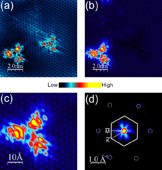
The STM topographic image and the map acquired at 78K for the sample bias voltage mV are shown in Figs. 1(a) and 1(b). We find two different defect images with clover- and triangular-shaped patterns superimposed on the atomically resolved periodic structure spreading over the entire surface area in the topographic STM image. In the image of Fig. 1(b) the clover-shaped pattern can still be seen, but not the triangular one. If we take a close look at the clover-shaped pattern in Fig. 1(c), we find the intensity modulation near the defect with a much longer wavelength than the surface lattice constant. A similar pattern has been observed in the pioneering STM study Urazhdin_PRB_02 and identified as a defect state induced by an excess Bi atom substituting the bottom Se site of the topmost quintuple layer. It was suggested that a resonance state is formed inside the bulk valence band due to the defect. Since the concept of topological insulator was not established at that time, we now need to revisit and reconsider the origin of the peculiar pattern in the STM image by taking into account the presence of the Dirac fermions with helical spin texture.
In Fig. 1(d) we show the fast Fourier transformation (FFT) of the image. Here the surface Brillouin zone (SBZ) boundaries are drawn from the obtained sharp FFT spots originated from the surface periodicity. The FFT image unambiguously tells us that an electron interference takes place as is seen from the flower shaped intensity distribution (Fig. 1(d)). The maximal intensity is seen to be along the direction of the scattering vector , exhibiting a node in the direction.
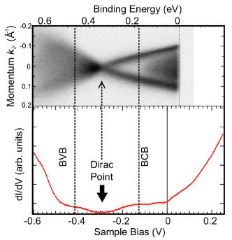
In order to further reveal the electron interference effect around the defects in Bi2Se3, we have performed the experiment at a liquid He temperature (4.5 K). Figure 2 shows the experimental local density of states (LDOS) measured as the differential tunneling conductance (STS) spectrum of Bi2Se3 surface. We find a V-shaped STS spectrum with a minimum at mV relative to the Fermi energy (), which corresponds to the Dirac point (DP). The slope of STS spectrum is seen to become much steeper below mV and above . By comparing the present STS spectrum with the reported ARPES energy dispersion Kuroda_PRL_10 , we find the bulk valence band (BVB) onset at meV leading to the enhancement of LDOS below this energy. The shoulder at meV coincides with the onset of bulk conduction band (BCB) as shown in Fig. 2.

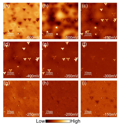
Figures 3(a)-3(i) represent the differential tunneling conductance images from to mV in the 50 nm nm scanning area. Here the clover-shaped defect again appears with a brighter contrast with respect to the rest part of the images in a limited bias window between and mV (Figs. 3(c)-3(f)), which is close to and a little below the DP. However, it loses contrast at higher voltages ( mV) and becomes even darker at mV (Figs. 3(a) and 3(b)).

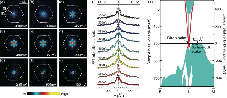
To quantify the observed electron interference effect and determine the relevant values, the FFT has been applied to the images in Figs. 4(a)-4(i). At first, we observe a characteristic continuous intensity distribution with sixfold symmetry inside the SBZ for , , , and mV, for which the clover-shaped patterns are observed in the corresponding images (Figs. 4(c)-4(f)). Of the four FFT images, the intensity is the most prominent at and mV, which coincides with the most distinct contrast in the clover-shaped pattern in Fig. 3(d) and 3(e). The characteristic six-fold pattern disappears above mV, where only a weak intensity remains around the SBZ center (Figs. 4(g)-4(i)). Below mV, the FFT patterns become less anisotropic and their intensity is weakened as the bias voltage decreases. It follows from the FFT analysis that the anisotropic interference is strongest between and mV, i.e., close to and slightly below the Dirac point.
To gain deeper insight into the origin of the unexpected interference pattern, the cross-sectional FFT patterns traced along direction are shown in Fig. 4(j). For the whole range of sample bias voltages, we observe the largest intensity at =0, which might originate from several extrinsic factors, such as a background noise whose modulation length would be much longer than the characteristic wavelength of the surface lattice periodicity and the electron interference.
On the topological insulator surface, the spins are locked with momenta, giving rise to helical Dirac fermions with lifted spin degeneracy. Owing to the strictly antiparallel spins at and , surface electrons are protected from backscattering, and no standing wave pattern arising from the interference with the backscattered wave can be observed for a single Dirac cone. On the other hand, there might be other scattering channels within the surface state cone with a finite parallel spin component, which could contribute to the scattering with small values of less than 0.2 Å-1 (the maximal radius of the cone is 0.1 Å-1). Although a detailed structure of surface state scattering is not resolved in the present data, the dominant contribution around =0 apparently originates from the extrinsic effect because a finite intensity at =0 persists and even enhances below mV, where the surface states are merged into the bulk valence band.
Let us now consider broad humps centered at Å-1, which are especially pronounced in the sample bias range from to mV as indicated by vertical bars in Fig. 4(j). The intensities in this cross sectional FFT profile are spread over a wide interval Å-1. Note that the FFT pattern is anisotropic, i.e., the intensity vanishes in the direction, see Figs. 4(c)-4(f). The observed magnitude of the scattering vector, Å-1, is too large to be explained by a scattering within the Dirac cone, especially near the DP. Besides, the profile is too broad to be explained by a scattering between the surface states well localized in . Also note that the intensity maxima of the hump are nearly independent of the bias voltage. Another important observation is that the hump almost disappears at 50 mV above the DP, which also excludes its origin from the surface state scattering. Since the scattering occurs at the near-surface defect, we need to consider both surface and bulk band structure to figure out a possible scattering channel other than the surface states of the Dirac cone.
We have performed a first principles calculation of the surface states with a slab of seven formula units with a two-component self-consistent (within the local density approximation) full-potential augmented plane wave method Krasovskii_PRB_99 . According to the theoretical band structure the DP is energetically located slightly below the bulk valence band maximum in the middle of the interval, whereas around the point the bulk band gap widens, so the states of the Dirac cone are energetically well separated from the bulk states with small vectors (Fig. 4(k)). The interference between a surface state with the lateral Bloch vector and a bulk state with caused by the scattering at the point defect results in spatial oscillations of LDOS with the wave vector . The possible transitions at the DP energy are seen to be centered at Å-1 in the direction. At the same time, in the direction such transitions are forbidden in a wide energy interval: the valence band maximum is located much lower in energy than in the direction. This striking anisotropy explains the negligible FFT intensity along line, which results in the flower-shaped distribution in Fig. 4. Since the bulk states are continuously distributed over the surface perpendicular momentum the interference pattern broadens, leading to a smeared hump in Fig. 4(j). Between the valence band maximum and the conduction band minimum there exists a large portion of the upper cone that does not energetically overlap with bulk states. This is consistent with the abrupt disappearance of the hump above mV (Fig. 4(j)). This means that the surface-bulk scattering is strongly suppressed above the DP, which supports our interpretation of the hump at Å-1 as due to the scattering into bulk states. A similar scattering may also occur via the bulk conduction band for -100 meV with a smaller scattering vector Å-1, which is beyond the resolution limit of this measurement. Most probably, it is this process that gives rise to the triangular-shaped pattern in Fig.1, as it appears in the topographic image and disappears in the dI/dV map.
In summary, we have shown by scanning tunneling microscopy and differential tunneling conductance measurements that a strong surface state – bulk continuum scattering occurs near the Dirac node at the surface of the three dimensional topological insulator Bi2Se3, contrary to the belief that the surface state in the bulk energy gap around point is protected from scattering Xia_NatPhys_09 . This may have implications for the construction of spintronic devices. In particular, it has been proposed to tune the DP at the top and the bottom surfaces of a thin film below and above the chemical potential in the dual-gate device configuration Yazyev_PRL_10 . To suppress the scattering one would have to separate both the lower and the upper Dirac cone from the bulk states. Also, in order to realize the anomalous Hall effect by an appropriate magnetic doping, one must precisely tune the chemical potential right at the Dirac point to achieve the surface insulating state by opening the energy gap Ru_Science_10 . Thus, we expect the present results to stimulate future band engineering in order to isolate the Dirac surface state from the bulk continuum and facilitate topological quantum transport.
We thank Shuichi Murakami of Tokyo Institute of Technology for valuable discussion. The ARPES measurement was performed with the approval of the Proposal Assessing Committee of HSRC (Proposal No. 09-A-52). This work was financially supported by the JSPS Grant-in-Aid for Scientific Research (B) 20340092.
References
- (1) C.L. Kane, and E.J. Mele, Phys. Rev. Lett. 95, 146802 (2005).
- (2) B.A. Bernevig and S.C. Zhang, Phys. Rev. Lett. 96, 106802 (2006).
- (3) B.A. Bernevig, T.L. Hughes, and S.C. Zhang, Science 314, 1757 (2006).
- (4) M. König, S. Wiedmann, C. Brüne, A. Roth, H. Buhmann, L.W. Molenkamp, X.L. Qi, S.C. Zhang, Science 318, 766 (2007).
- (5) D. Hsieh, D. Qian, L. Wray, Y. Xia, Y.S. Hor, R.J. Cava and M.Z. Hasan, Nature 452, 970 (2008).
- (6) D. Hsieh, Y. Xia, L. Wray, D. Qian, A. Pal, J.H. Dil, J. Osterwalder, F. Meier, G. Bihlmayer, C.L. Kane, Y.S. Hor, R.J. Cava, and M.Z. Hasan, Science 323, 919 (2008).
- (7) Y. Xia, D. Qian, D. Hsieh, L. Wray, A. Pal, H. Lin, A. Bansil, D. Grauer, Y.S. Hor, R.J. Cava and M.Z. Hasan, Nature Phys. 5, 398 (2009).
- (8) Y.L. Chen, J.G. Analytis, J.-H. Chu, Z.K. Liu, S.-K. Mo, X.L. Qi, H.J. Zhang, D.H. Lu, X. Dai, Z. Fang, S.C. Zhang, I.R. Fisher, Z. Hussain, Z.-X. Shen, Science 325, 178 (2009).
- (9) K. Kuroda, M. Arita, K. Miyamoto, M. Ye, J. Jiang, A. Kimura, E. E. Krasovskii, E. V. Chulkov, H. Iwasawa, T. Okuda, K. Shimada, Y. Ueda, H. Namatame, and M. Taniguchi, Phys. Rev. Lett. 105, 076802 (2010). The energy offset of the Dirac point in the ARPES spectrum by 0.05 eV relative to its location in the STS spectrum is most probably due to the molecular adsorption during the measurement, which is known to slightly change the surface state energy.
- (10) L. Fu, and C.L. Kane, Phys. Rev. B 76, 045302 (2007).
- (11) H. Zhang, C.X. Liu, X.L. Qi, X. Dai, Z. Fang, and S.C. Zhang, Nature Phys. 5, 438 (2009).
- (12) D. Hsieh, Y. Xia, D. Qian, L. Wray, J.H. Dil, F. Meier, J. Osterwalder, L. Patthey, J.G. Checkelsky, N.P. Ong, A.V. Fedorov, H. Lin, A. Bansil, D. Grauer, Y.S. Hor, R.J. Cava, and M.Z. Hasan, Nature 460, 1101 (2009).
- (13) A. Nishide, A.A. Taskin, Y. Takeichi, T. Okuda, A. Kakizaki, T. Hirahara, K. Nakatsuji, F. Komori, Y. Ando, and I. Matsuda, Phys. Rev. B 81, 041309(R) (2010).
- (14) J.G. Checkelsky, Y.S. Hor, M.H. Liu, D.X. Qu, R.J. Cava, and N.P. Ong, Phys. Rev. Lett. 103, 246601 (2009).
- (15) J.G. Analytis, J.H. Chu, Y. Chen, F. Corredor, R.D. McDonald, Z.X. Shen, and I.R. Fisher, Phys. Rev. B 81, 205407 (2010).
- (16) K. Eto, Z. Ren, A.A. Taskin, K. Segawa, and Y. Ando, Phys. Rev. B 81, 195309 (2010).
- (17) N.P. Butch, K. Kirshenbaum, P. Syers, A.B. Sushkov, G.S. Jenkins, H.D. Drew, and J. Paglione, Phys. Rev. B 81, 241301(R) (2010).
- (18) S. Urazhdin, D. Bilc, S.H. Tessmer, S.D. Mahanti, T. Kyratsi, and M.G. Kanatzidis, Phys. Rev. B 66, 161306 (2002).
- (19) Y.S. Hor, A. Richardella, P. Roushan, Y. Xia, J.G. Checkelsky, A. Yazdani, M.Z. Hasan, N.P. Ong, and R.J. Cava, Phys. Rev. B 79, 195208 (2009).
- (20) T. Zhang, P. Cheng, X. Chen, J.F. Jia, X. Ma, K. He, L. Wang, H. Zhang, X. Dai, Z. Fang, X. Xie, and Q.K. Xue, Phys. Rev. Lett. 103, 266803 (2009).
- (21) Z. Alpichshev, J.G. Analytis, J.-H. Chu, I.R. Fisher, Y.L. Chen, Z.X. Shen, A. Fang, and A. Kapitulnik, Phys. Rev. Lett. 104, 016401 (2010).
- (22) E.E. Krasovskii, F. Starrost, and W. Schattke, Phys. Rev. B 59, 10504 (1999).
- (23) O.V. Yazyev, J.E. Moore, and S.G. Louie, Phys. Rev. Lett. 105, 266806 (2010).
- (24) R. Yu, W. Zhang, H.J. Zhang, S.C. Zhang, X. Dai, Z. Fang, Science 329, 61 (2010).