Transport in disordered two-dimensional topological insulator
Abstract
We study experimentally the transport properties of ”inverted” semiconductor -based quantum well, which is related to the two-dimensional topological insulator, in diffusive transport regime. We perform nonlocal electrical measurements in the absence of the magnetic field and observe large signal due to the edge states. It demonstrates, that the edge states can propagate over long distance , and, therefore, there is no difference between local and non local electrical measurements in topological insulator. In the presence of the in-plane magnetic field we find strong decrease of the local resistance and complete suppression of the nonlocal resistance. We attribute this observation to the transition between topological insulator and bulk metal induced by the in-plane magnetic field.
pacs:
73.43.-f, 73.43.QtRecently, a novel class of the topological state of a quantum matter has emerged, called topological insulator kane ; bernevig ; Qi ; konig . The first famous example of the two dimensional topological insulator (2DTI) is the integer quantum Hall effect (QHE) state on the resistance minima prange . Such system represents the 2D electron gas in the presence of the strong perpendicular magnetic field, when all current is carried by the edge states, while electrons in the bulk region are localized. The number of the edge states are determined by the Landau level filling factor . The edge states are unidirectional because of the breaking of the time-reversal (TR) symmetry due to the magnetic field and robust against impurity scattering. Note, that disorder plays the crucial role in establishment of the Hall plateau in the finite region of the magnetic field or electron density.
Another class of 2DTI is the quantum spin Hall effect state, which can be realized in 2D system with strong spin-orbit interaction in the absence of the magnetic field kane ; bernevig ; Qi ; konig . It has been shown that an ”inverted” semiconductor HgTeCdTe quantum well bernevig ; konig , possess the insulating phase having the gap in the bulk electron spectrum and a single pair of counterpropagating or helical edge states for the two opposite spin polarizations. Remarkable consequence of the presence of the edge states in ballistic 2DTI is a quantized longitudinal resistance , which has been observed in micrometer scale Hall bars konig . The edge states are expected to be insensitive to weak, nonmagnetic impurity scattering due to destructive interference between two backscattering paths of the helical edge states ( see review hasan ). It is worth noting that the backscattering does not destroy the edge states, therefore any 2DTI sample represents almost ideal natural one dimensional (1D) wire localized near the sample edge.
In this letter we present an experimental study of the transport properties of ”inverted” -based quantum well which possesses a pair of counter-propagating or helical edge states strongly mixed by spin flip scattering. When the Fermi level passes the bulk insulating gap, the devices revel unusual behaviour, which is characterized by high resistance with metallic temperature dependence. Since the scattering between helical edge states is topologically protected due to time reversal symmetry, we attribute high level of the resistance to spin flip scattering induced by spin-orbital interaction, or two-particle backscattering, which breaks TR symmetry. Therefore, the edge state at the periphery of the disordered TI constitutes the single one-dimensional wire. We perform nonlocal electrical measurements and dramatically demonstrate that edge-state transport truly exists over macroscopic distance of in the absence of the magnetic field. The in-plane magnetic field strongly suppresses local magnetoresistance an completely destroys resistance measured in nonlocal configuration. This observation is attributed to in-plane magnetic field induced transition from 2D TI state to bulk metal state.
The quantum wells with the (013) surface orientation and a different thickness of 8 and 8.3 nm were prepared by molecular beam epitaxy. A detailed description of the sample structure has been given in kvon ; gusev . The schematic view of a typical micro-fabricated device is shown in Figures 1a,b. Device consists of 3 narrow ( of width) channels (segments) with different lengths ( consequently), and 8 side branches (probes). The ohmic contacts to the two-dimensional gas were formed by the in-burning of indium. To prepare the gate, a dielectric layer containing 100 nm and 200 nm was first grown on the structure using the plasmochemical method. Then, the TiAu gate was deposited. Dimension of the gate is macroscopic (), which is crucial for creating of the long length edge states. The density variation with gate voltage was . The magnetotransport measurements in the described structures were performed in the temperature range 0.050-4.1 K and in magnetic fields up to 15 T using a standard four point circuit with a 2-3 Hz ac current of 0.1-1 nA through the sample, which is sufficiently low to avoid the overheating effects.
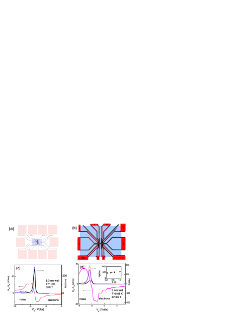
Figures 1c,d show the data in zero magnetic field and standard quantum Hall effect measurements in 8.3 nm (c) and 8.0 nm (d) HgTe wells, which indicate high quality of our sample. The measured mobility of electrons is approximately and mobility of holes , which is comparable to that found in HgTe well of wider width kvon ; gusev . Sweeping gate voltage from the positive to the negative value than depopulates electrons states and populates hole states. We may see it from Hall resistance behaviour: changes smoothly through zero from its negative quantized value on the electron side to a positive quantized value on the hole side, whereas moves from a zero on the electron side through a maximum at the bulk energy gap to another zero-minimum on the hole side. Note that the resistance at maxima sharply decreases with magnetic field.
In the following we will concentrate on the electronic behavior around the bulk energy gap in zero magnetic fields and at low temperatures. It is expected that the transport properties in this region are determined by pair of counterpropagating or helical edge states states for the two opposite spin polarizations, and resistance is quantized at value . However, we find finite resistance (8.3 nm well), which is significantly higher than . This agrees with previous results obtained in samples with a length of , which has been attributed to inelastic scattering between helical edge states konig2 . Nonuniversality of the resistance in the presence of the spin dephasing has been predicted by various theoretical models jiang ; strom . Inelastic mechanism, however, disagrees with absence of the temperature dependence of the resistance peak. The origin of the resistance is determined by the behaviour of the contacts regions, similar to the conventional quantum Hall effect. Contacts are assumed to be a thermal reservoirs buttiker , when full mixing of electron spin states can occur. Note, that in contrast to the standard QHE, when mixing of edge states occurs within metallic Ohmic contacts, in our samples potential mixing is provided by 2D electron gas in the region outside of the metallic gate due to finite bulk conductivity. Fig. 1b illustrates such geometry. We may see that the length of the edge states are determined by the perimeter of the sample part covered by metallic gate (mostly side branches) rather that the length of the microbridge. We calculate the length of 1D wires between probe contacts and find that it exceeds 1.0 mm. For such macroscopic distance it is naturally to expect strong backscattering between states with two opposite spin polarizations due to spin flip scattering or scattering by magnetic impurities. Elastic magnetic scattering is unlikely to explain our data, because the background magnetic impurity content of MBE machine is very low. The high resistance can be attributed to the spin flip scattering induced by spin-orbital interaction, somewhat similar to transition between spin split states in the quantum Hall effect regime, considered in the model khaetskii . Such elastic backscattering should lead, however, to localization, and T-dependent resistance. This is contrary to our observations. The alternative model based on two-particle excitation strom ; xu ; wu leads to suppression of localization, since the inelastic dephasing time becomes comparable with backscattering time, which can cancel out the temperature effect.
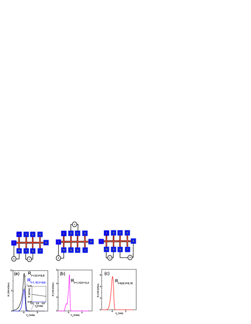
Note that the 2DTI in zero magnetic field is equivalent to the QHE state at near charge neutrality point in graphene considered in the model abanin . Within this model transport in graphene at strong magnetic field is dominated by the pair of gapless edge excitations, which however, have magnetic nature. In the absence of transport through the bulk, if both edges carry the same current, the resistance is , where is the mean free path for 1D backscattering, L is the length of 1D channel between contacts, or thermal reservoirs, which in our case are related to 2D electron gas. Comparing this model, which applies equally well to the transport in 2DTI in zero magnetic field, with our results we obtain . Estimation of the two-particle backscattering predicts corresponding length of the order of few meters ostrovsky . More theoretical work is desirable in order to understand spin flip dephasing mechanism in TI. We measured several samples from different wafers and found that peak resistance is varied from 300 kOhm to 2 MOhm, which likely stems from variation of the disorder parameters. The application of the current between any pair of the probes creates net current along the sample edge, and can be detected by any other pair of the voltage probes. In general, there is no difference between local and non local electrical measurements in topological insulator. Fig.2 shows several traces for local and nonlocal resistance taken at different configurations for 8 nm HgTe well. The data demonstrate that the nonlocal resistance is negligibly small in the region with homogeneous 2D electron and hole gas, outside of the TI peak, as expected for classical dissipative transport (see insert to figure 2a). The nonlocal resistance in TI regime has comparable amplitude and qualitatively the same position and width of the peak. The occurrence of the nonlocal resistance of comparable amplitude implies that potential difference extend over macroscopic distance away from dissipative bulk current path. It is only possible, if the bulk conductivity is completely suppressed and conductivity of the TI sample is determined by edge states. To analyze nonlocal resistance value we employ simple model which describes sample resistance as combination of resistors along sample edge, assuming that resistance value is proportional to the length of the 1D channel (Figure 2). For realistic configuration of the sample, shown in figure 1, we estimate this ratio , which roughly agrees with experimental value. Note that in ballistic case the nonlocal transport indeed has been observed in mesoscopic samples roth , when nonlocal resistance have been obtained within the general Landauer-Büttiker formalism buttiker .
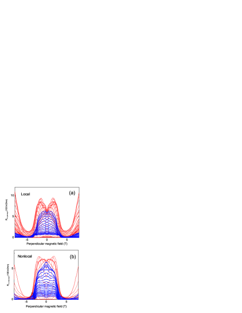
Application of the strong perpendicular, and in-plane magnetic field would be important to establish the physics of topological insulators, and one may ask if they can also exhibit other interesting phenomena. Previous experiments in ballistic structures konig demonstrated sharp spike at B=0 and decrease of the conductance with increasing of perpendicular magnetic field . No magnetoresistance has been observed in the presence of the in-plane magnetic field . This observation has been attributed to the opening of the gap between edge states due to Zeeman splitting. Alternative scenario has been suggested in paper maciejko , when orbital effects and effects of disorder have been included. In disordered TI we find different behaviour. Figure 3 shows the magnetoresistance in local and nonlocal configurations for different gate voltages, when the Fermi level passes from electron to hole side of the peak in figure 2. It is worth noting remarkable similarity between these two sets of curves. It confirms again that the transport in TI occurs only at the periphery of the sample. The magnetoresistance exhibits several features with magnetic field. First, sample reveals the spike a low magnetic field, which, however, has a smaller magnitude that one in ballistic devices, and shows remarkable evolution with gate voltage. Second, magnetorsistance exhibits several jumps and sawtooth oscillations with magnetic field, which are very different from conventional universal conductance fluctuations in 1D wires stone . Third, we may see giant magnetooscillations with magnitude , which is also very unusual in 1D wires. Finally, strong decrease of the resistance at T is observed, moreover, in electronic side of the peak, resistance approaches zero, which corresponds minima in the quantum Hall effect regime. Such rich magnetorsistance behavior requires more detailed analysis and comparison with theory, and indeed it will be done in forthcoming publications.
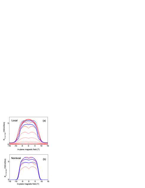
The Figure 4 shows the evolution of the local and nonlocal magnetoresistance with gate voltage in the presence of the in-plane magnetic field. Again we may see strong similarity between these two sets of magetoresistance curves. In contrast to previous measurements in ballistic devices konig2 we observe large positive magnetoresistance within 2 T. In magnetic field both resistances dramatically drop with increase of the in-plane field. Examination of traces in Fig 4 in magnetic field higher than 10 T immediately reveals drastic difference between and nonlocal resistance: the nonlocal resistance data with negligible small value in this region corresponds to large (10-50 kOhm) value of . Note, that in perpendicular magnetic field both resistances have comparable values in strong B ( figure 3). Thus, the external parallel magnetic field strongly suppresses and completely destroys nonlocal resistance. The nonlocal resistance is very small in the presence of the bulk dissipative transport. Therefore it is naturally suggest, that in-plane magnetic field destroys the edge state transport and at the same time induces electronic states in the bulk. Alternatively we may suggest that in-plane field induces unidirectional edge states similar to QHE state in perpendicular magnetic field. These states indeed are dissipationless, and voltage drop between probe contacts is zero. However, within this scenario, local should be zero too, which disagrees with our observation (see Fig.4a). Therefore our data demonstrate the existence of the in-plane magnetic field induced transition between 2DTI state and bulk metal state. More experimental work and theoretical effort has to be done in order to understand the origin of these emergent phenomena.
In summary, we report on the observation of disordered 2DTI state in HgTe quantum wells in zero magnetic field, and the emergence of conductive bulk state in the presence of the in-plane magnetic field. We demonstrate the similarity between local and nonlocal resistance measurements in zero and perpendicular magnetic field in TI regime. These data give the evidence that in realistic samples edge-state transport truly exists over macroscopic distance of in the absence of the magnetic field.
We thank O.E.Raichev and I.V.Gorny for helpful discussions. A financial support of this work by FAPESP, CNPq (Brazilian agencies), USP-COFECUB (Uc Ph 109/08), FAPESP-CNRS, RFBI (09-02-00467a and ofi-m) and RAS programs ”Fundamental researches in nanotechnology and nanomaterials” and ”Condensed matter quantum physics” is acknowledged.
References
- (1) C. L. Kane and E. J. Mele, Phys. Rev. Lett. 95, 146802 (2005).
- (2) B.A.Bernevig and S. C. Zhang, Phys. Rev. Lett. 96, 106802 (2006); B. A. Bernevig, T. L. Hughes, and S. C. Zhang, Science 314, 1757 (2006).
- (3) X. L. Qi, R. D. Li, J. D. Zang, and S. C. Zhang, Science 3̱23, 1184 (2009).
- (4) M. König et al, Science 318, 766 (2007).
- (5) The Quantum Hall Effect, 2nd Ed., edited by Richard E. Prange and Steven M. Girvin (Springer-Verlag, New York, 1990).
- (6) M. Z. Hasan, C. L. Kane, Rev.Mod.Phys. 82, 2045 (2010); X-L. Qi, S-C. Zhang, arXiv:1008.2026v1 (unpublished)
- (7) Z. D. Kvon, E. B. Olshanetsky, D. A. Kozlov, et al., Pis’ma Zh. Eksp. Teor. Fiz. 87, 588 (2008) [JETP Lett. 87, 502 (2008)].
- (8) G. M. Gusev et al, Phys. Rev. Lett. 104, 166401, (2010).
- (9) M. König et al, J. Phys. Soc. Jpn. 77, 031007 (2008).
- (10) H.Jiang, S.Cheng, Q.F.Sun, X.C.Xie, Phys. Rev. Lett. 103, 036803 (2009).
- (11) A.Ström, H.Johannesson, G.I.Japaridze, Phys. Rev. Lett. 104, 256804 (2010).
- (12) M. Büttiker, Phys. Rev. Lett. 57, 1761 (1986).
- (13) A.V.Khaetskii, Phys. Rev. B 45, 13777 (1992).
- (14) C. Xu, J.E.Moore, Phys. Rev. B 73, 045322 (2006).
- (15) C.Wu, B.A.Bernevig, S-C.Zhang, Phys. Rev. Lett. 96, 106401 (2006).
- (16) D.A. Abanin et al, Phys. Rev. Lett. 98, 196806 (2007).
- (17) P. M. Ostrovsky, I.V. Gornyi, A. D. Mirlin, Phys. Rev. Lett. 105, 036803 (2010).
- (18) A. Roth et al, Science 325, 294 (2009).
- (19) A. D. Stone, Phys. Rev. Lett 54 2692 (1985); G.Timp et al, Phys. Rev. Lett. 59, 732 (1987).
- (20) J. Maciejko, X-L. Qi, and S-C. Zhang, Phys. Rev. B 82, 155310 (2010).