Ultrafast nano-focusing with full optical waveform control
Abstract
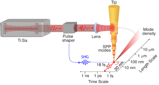
The spatial confinement and temporal control of an optical excitation on nanometer length scales and femtosecond time scales has been a long-standing challenge in optics. It would provide spectroscopic access to the elementary optical excitations in matter on their natural length and time scales Brixner et al. (2005) and enable applications from ultrafast nano-opto-electronics to single molecule quantum coherent control Assion et al. (1998). Previous approaches have largely focused on using surface plasmon polariton (SPP) resonant nanostructures Aeschlimann et al. (2007) or SPP waveguides Cao et al. (2010); Durach et al. (2007) to generate nanometer localized excitations. However, these implementations generally suffer from mode mismatch Schuck et al. (2005) between the far-field propagating light and the near-field confinement. In addition, the spatial localization in itself may depend on the spectral phase and amplitude of the driving laser pulse thus limiting the degrees of freedom available to independently control the nano-optical waveform. Here we utilize femtosecond broadband SPP coupling, by laterally chirped fan gratings, onto the shaft of a monolithic noble metal tip, leading to adiabatic SPP compression and localization at the tip apex Stockman (2004); Babadjanyan et al. (2000). In combination with spectral pulse shaping Weiner (2000); Xu et al. (2006) with feedback on the intrinsic nonlinear response of the tip apex, we demonstrate the continuous micro- to nano-scale self-similar mode matched transformation of the propagating femtosecond SPP field into a 20 nm spatially and 16 fs temporally confined light pulse at the tip apex. Furthermore, with the essentially wavelength and phase independent 3D focusing mechanism we show the generation of arbitrary optical waveforms nanofocused at the tip. This unique femtosecond nano-torch with high nano-scale power delivery in free space and full spectral and temporal control opens the door for the extension of the powerful nonlinear and ultrafast vibrational and electronic spectroscopies to the nanoscale Kubo et al. (2005); Bartels et al. (2000).
In order to achieve the goal of an efficient nanometer confined femtosecond light source with independent spatial localization and temporal control of the optical field, and which can freely be manipulated in 3D, the use of the unique properties of surface plasmon polaritons (SPP’s) has long been discussed as a potential solution. It is well established that the strong surface field localization and size and shape dependent resonances of SPP’s as electromagnetic surface waves associated with collective charge density oscillations at noble metal-dielectric interfaces allow for sub-wavelength spatial control of even broadband optical fields Schuller et al. (2010). Elegant solutions to overcome the SPP diffraction limit Yin et al. (2005) and achieve nano-focusing based on interference of localized SPP modes exist in the form of specially arranged cascaded, percolated, or self-similar chains of metal nanostructures as optical antennas Volpe et al. (2010); Aeschlimann et al. (2007); Gunn et al. (2010). However, the achievable optical waveforms at the nano-focus are often constrained by the phase relationship between the spectral modes already necessary to achieve the 3D nano-focusing Durach et al. (2007). This limits the degrees of freedom for full and structurally independent spatial and temporal control of the nano-focused field not . Related challenges persist for nano-devices in the form of tapered grooves, wires, or wedges Volkov et al. (2009); Fang et al. (2009); Cao et al. (2010). While they allow for nano-focusing via their propagating SPP waveguide properties with favorable power transfer, scalability, and broad bandwidth, many such geometries do not allow for full 3D spatial localization independent of spectral phase Durach et al. (2007); Cao et al. (2010), and a substrate-based design Volkov et al. (2009) makes spatially and spectrally non-dispersive nano-focusing difficult.
In contrast, a 3D tapered tip as an SPP waveguide stands out due to its unique topology as a cone. As has been proposed theoretically Babadjanyan et al. (2000); Stockman (2004), and recently demonstrated experimentally Ropers et al. (2007a); Neacsu et al. (2010); Sadiq et al. (2011), that geometry allows for true 3D focusing into a excitation volume as small as a few 10’s of nm size. The divergence of the effective index of refraction with decreasing cone radius experienced by an SPP propagating towards the apex leads to a continuous transformation of cylindrical modes and thus near adiabatic SPP nano-focusing into the apex of the tip.

Despite some constraints on power transfer from the propagating SPP to the apex localized excitation due to SPP absorption and reflection, this effect is only weakly wavelength-dependent and the nano-focusing mechanism is expected to be independent of spectral phase Issa and Guckenberger (2007). Therefore, for sufficiently broadband SPP excitation, independent nanometer spatial and femtosecond temporal control should be achievable.
As shown conceptually in Fig. 1 (for a detailed experimental description see supplementary material) for the experiment, laser pulses from a 10 fs Ti:Sa oscillator are passed through a pulse shaper for spectral amplitude and phase control Weiner (2000), and focused onto the shaft of a monolithic Au tip at 25∘ incidence using a long working distance objective. The tips are formed through an electrochemical etching process, resulting in 10 nm apex radius, as discussed previously Neacsu et al. (2010). SPP’s are launched onto the tip using a laterally chirped fan-shaped plasmonic grating element, allowing tunable broadband grating-coupling, in order to overcome the momentum mismatch between the incident wavevector and the SPP Ropers et al. (2007a). The light emission from the tip apex is collected through a separate objective, with spatial and spectral filtering, and detected using a spectrometer with a N2(l)-cooled CCD.

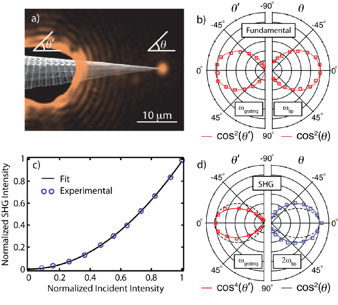
Fig. 2a) shows an SEM image of a tip with a broadband grating superimposed with an optical image showing the far-field illumination incident on the grating and subsequent re-radiation of the spatially confined apex SPP field from a region 25 nm in size, as demonstrated by scanning the tip over a nanometer edged reference sample Neacsu et al. (2010). The characteristic polarization anisotropy of both the apex-emitted fundamental and localized second-harmonic generation (SHG) light, arising from the broken axial symmetry at the apex Neacsu et al. (2005), show the expected intensity dependence expected for a point dipole emitter. Note the different fundamental grating input polarization dependencies with dependence for fundamental apex emission, and dependence for SHG emission. Typically, for 30 mW incident light on the grating we estimate the total apex emission to be 100 W fundamental and 10 pW SHG.
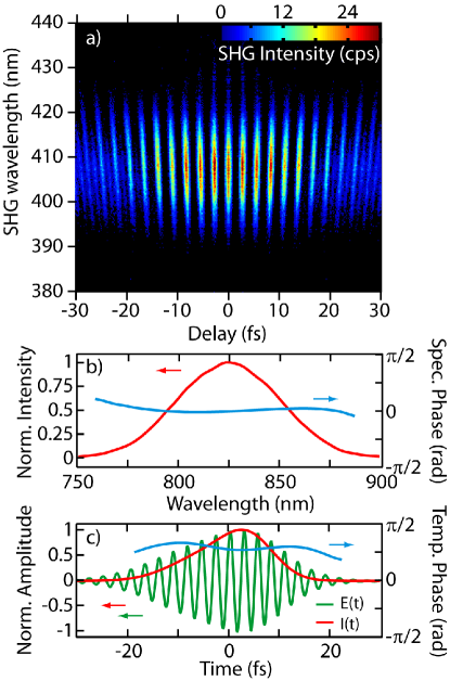
After optimizing the grating illumination and coupling parameters for maximum coupling bandwidth or SHG intensity depending on application, the optical waveform of the nano-focus is controlled using spectral pulse shaping with SHG as the feedback parameter for the multiphoton intrapulse interference phase scan (MIIPS) algorithm used Xu et al. (2006). The MIIPS-optimized pulses are then characterized via interferometric frequency resolved optical gating (IFROG) Anderson et al. (2010) and the pulse transient is reconstructed with phase and amplitude information from the DC portion of the spectrogram using a standard FROG retrieval algorithm. The pulse replicas as required for the IFROG autocorrelation measurements are themselves generated with the pulse shaper.

Fig. 3a) shows an IFROG trace for few-femtosecond broadband nanofocusing with corresponding reconstructed spectral (Fig. 3b) and temporal (Fig. 3c) intensity profiles (red) and phase (blue). After MIIPS optimized flattening of the spectral phase to within 0.1 rad for the primary portion of the pulse, we obtain a transform-limited pulse with a duration of 16 fs for the given coupling bandwidth of FWHM 60 nm in this case. The result is shown in Fig. 3c) along with the temporal electric field transient obtained (green).

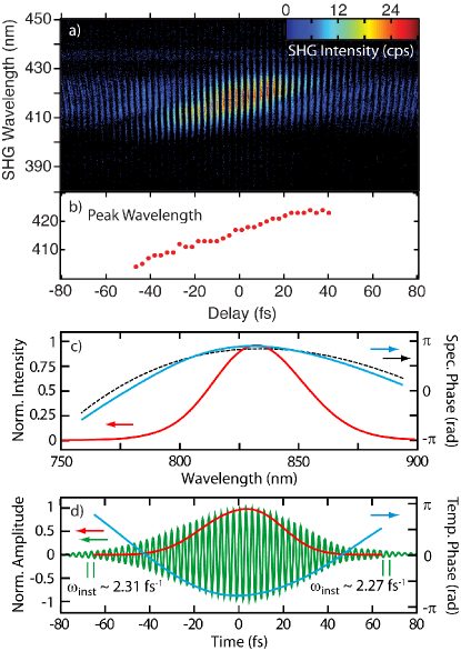
To demonstrate the capability to nanofocus a femtosecond pulse of arbitrary waveform we generate a chirped pulse with a group delay dispersion of fs2 at the tip apex as an example. Fig. 4a) shows the measured XFROG trace using a transform limited 16 fs pulse with identical spectrum as reference. Fig. 4b) shows the associated temporal variation in instantaneous carrier wavelength. The reconstructed spectral intensity of the chirped pulse is shown in Fig. 4c) (red). The comparison and good agreement between the reconstructed phase (solid blue) and the applied phase function of fs2 (black dashed) as set by the pulse shaper show the high degree of accuracy of this procedure. Shown in Fig. 4d) are the corresponding time-domain intensity (red), phase (blue), and electric field transient (green) with the shift in the instantaneous frequency indicated across the chirped pulse.
These two examples demonstrate the unique ability of the 3D tapered tip for simultaneous SPP nanofocusing and optical waveform control compared to the alternative geometries and approaches mentioned above. By relying on the diverging index of refraction experienced by propagating SPP’s with decreasing cone radius, the mode transformation into a nanoscale excitation at the tip apex remains continuous and impedance matched Stockman (2004), while the uniform taper surface prevents the otherwise typical scattering and reflection losses at structural discontinuities. Due to the radial symmetry and decreasing SPP group velocity, full nanoconfinement in all spatial dimensions is achieved Neacsu et al. (2010); Berweger et al. (2010); Sadiq et al. (2011).
In addition, the tips allow for the desired broadband excitation necessary for true femtosecond optical control. As predicted theoretically, the nanofocusing efficiency is maximal in the 800 nm range for a tip cone angle of 14∘ Issa and Guckenberger (2007) as used in our experiment with previously demonstrated monochromatic nanofocusing efficiencies of up to 9 Berweger et al. (2010). Since the SPP nanofocusing mechanism does not rely on localized SPP resonance conditions, its weak wavelength dependence provides phase-independent nanofocusing over a broad wavelength range as desired for ultrafast pulses as short as just a few femtoseconds Issa and Guckenberger (2007). As a direct consequence, the spectral phase and amplitude of the coupled pulse are retained as degrees of freedom that can be controlled independently.
In contrast to other nano-focusing structures based either on localized plasmon resonances Aeschlimann et al. (2007) or propagating SPP modes Durach et al. (2007); Cao et al. (2010) which exhibit a dependence of the spatial localization on the spectral and phase characteristics of the excitation field, we control the pulse duration and optical waveform at the tip apex via deterministic pulse shaping, as opposed to adaptive techniques, thus reducing the computation duration of the optimization procedure as well as algorithm complexity. Furthermore, in order to characterize the designed nanofocus waveform both in terms of spectral phase and amplitude, the nanofocused apex field conveniently generates local SHG due to the broken axial symmetry of the apex Neacsu et al. (2005). This structurally intrinsic coherent nonlinear response thus enables a direct means to apply appropriate spectrogram-based nonlinear wavemixing pulse characterization techniques (e.g., FROG, XFROG) for the complete optical waveform determination and optimization without the requirement for a separate nonlinear material or asymmetric structure for nonlinear optical frequency conversion.
The theoretical limit for the shortest attainable pulse duration at the tip apex is determined only by the coupling bandwidth and the dephasing time in the case of spectral overlap with a localized SPP of the tip apex. While the tips used in our off-resonant experiments shown here typically exhibit SPP resonances in the vicinity of 650 nm, the use of localized tip SPP’s with measured dephasing times of up to fs Anderson et al. (2010) can provide additional capability for tailoring the optical waveform with higher field enhancement, albeit at the expense of minimal pulse duration.
The details of the nanofocusing mechanism and the degree of adiabaticity are not yet completely understood as the optimal nanofocusing conditions require minimization of both SPP propagation damping and reflection losses, which increase and decrease with adiabatic conditions, respectively. This includes the propagation induced dispersion which is of particular interest for femtosecond nanofocusing. However, considering a group velocity dispersion of 0.4 fsm for an SPP propagating on a flat surface, the dispersion introduced by a propagation length of 20 m is expected to be small. This is in good agreement with comparison of grating-coupled and free-space MIIPS measurements showing little dispersion introduced by grating-coupling and subsequent SPP propagation and nanofocusing, although some tip-to-tip variability is observed. While arbitrary dispersion could be compensated within the capability of the pulse shaper using MIIPS, the apparent low dispersion provides favorable conditions for pulse optimization and characterization by yielding already large initial SHG levels.
The use of a grating as coupling element can provide high coupling efficiencies, but some scattering losses are inevitable. The fan-shaped gratings developed for this work enable a high coupling bandwidth with FWHM of up to nm (see supplementary material). Improvements in the form of grating structures with optimized groove depth and holographic geometries, chirped gratings including Bragg reflectors Lopez-Tejeira et al. (2007), broadband coupling via fabricated micro-prism onto the tip shaft Sánchez et al. (2002), spatial pulse shaping in the far-field excitation focus Piestun and Miller (2001), and tip fabrication with reduced surface roughness could further improve the tip performance for nanofocus optical waveform control. Without the need for resonance behavior in order for spatial localization to occur, the process can be extended to a wide range of wavelengths, limited in principle only by material damping at short wavelengths, and taper angle and reduced spatial field confinement at long wavelengths.
In summary, we have demonstrated independent nanometer spatial and femtosecond temporal optical waveform control, enabled by nanoscale field concentration via adiabatic SPP nanofocusing into monolithic gold tips, which is intrinsically broadband and independent of the instantaneous frequency and spectral phase of the excitation field. The in principle impedance matched far-field to near-field mode transformation allows for efficient power transfer into a nanoconfined volume at the tip apex. This light source with arbitrary waveform control at the nanoscale is of a fundamentally new quality compared to both conventional far- and near-field sources. It allows for the systematic extension of near background-free scanning probe microscopy Berweger et al. (2010); De Angelis et al. (2009); Sadiq et al. (2011) to the nanoscale implementation of many forms of nonlinear and ultrafast spectroscopies for spatio-temporal imaging Terada et al. (2010). This offers all-optical access to the study of nonequilibrium carrier and lattice excitations and their correlations on the level of their natural femtosecond time and nanometer length scales, thus providing unprecedented microscopic insight into the origin of complex biological, organic, or correlated electron materials. It allows for quantum coherent control of chemical reactions Assion et al. (1998) on the nanoscale, quantum information processing, provides a tool for nano-photonic circuit analysis, and, with the high field compression, new avenues for extreme nonlinear optics such as higher harmonic generation Bartels et al. (2000) or femtosecond electron pulse generation Ropers et al. (2007b).
Acknowledgements
We would like to acknowledge valuable discussions with Mark Stockman, Christoph Lienau, and Hrvoje Petek as well as funding from the National Science Foundation (NSF CAREER grant CHE 0748226).
Author contributions
S.B., X.G.X., and M.B.R. conceived the experiments as carried out and analyzed by S.B. and J.M.A. using the pulse shaper designed and built by X.G.X.; R.L.O. and S.B. designed the grating tips which were fabricated by R.L.O.; S.B., J.M.A., and M.B. R. prepared the manuscript. S.B. and J.M.A. contributed equally to this work.
References
- Brixner et al. (2005) T. Brixner, F. J. G. J. Schneider, and W. Pfeiffer, Phys. Rev. Lett. 95, 093901 (2005).
- Assion et al. (1998) A. Assion, T. Baumert, M. Bergt, T. Brixner, B. Kiefer, V. Seyfried, M. Strehle, and G. Gerber, Science 282, 919 (1998).
- Aeschlimann et al. (2007) M. Aeschlimann, M. Bauer, D. Bayer, T. Brixner, F. J. Garcia de Abajo, W. Pfeiffer, M. Rohmer, C. Spindler, and F. Steeb, Nature 446, 301 (2007).
- Cao et al. (2010) L. Cao, R. A. Nome, J. M. Montgomery, S. K. Gray, and N. F. Scherer, Nano Lett. 10, 3389 (2010).
- Durach et al. (2007) M. Durach, A. Rusina, M. I. Stockman, and K. Nelson, Nano Lett. 7, 3145 (2007).
- Schuck et al. (2005) P. J. Schuck, D. P. Fromm, A. Sundaramurthy, G. S. Kino, and W. E. Moerner, Phys. Rev. Lett. 94, 017402 (2005).
- Stockman (2004) M. I. Stockman, Phys. Rev. Lett. 93, 137404 (2004).
- Babadjanyan et al. (2000) A. J. Babadjanyan, N. L. Margaryan, and K. V. Nerkararyan, J. Appl. Phys. 87, 3785 (2000).
- Weiner (2000) A. M. Weiner, Rev. Sci. Intr. 71, 1929 (2000).
- Xu et al. (2006) B. Xu, J. M. Gunn, J. M. Dela Cruz, V. V. Lozovoy, and M. Dantus, J. Opt. Soc. Am. B 4, 750 (2006).
- Kubo et al. (2005) A. Kubo, K. Onda, H. Petek, Z. Sun, Y. S. Jung, and H. K. Kim, Nano Lett. 5, 1123 (2005).
- Bartels et al. (2000) R. Bartels, S. Backus, E. Zeek, L. Misoguti, G. Vdovin, I. P. Christov, M. M. Murnane, and H. C. Kapteyn, Nature 406, 164 (2000).
- Schuller et al. (2010) J. A. Schuller, E. S. Barnard, W. Cai, Y. C. Jun, J. S. White, and M. L. Brongersma, Nat. Mater. 9, 193 (2010).
- Yin et al. (2005) L. Yin, V. K. Vlasko-Vlasov, J. Pearson, J. M. Hiller, J. Hua, U. Welp, D. E. Brown, and C. W. Kimball, Nano Lett. 5, 1399 (2005).
- Volpe et al. (2010) G. Volpe, G. Molina-Terrizia, and R. Quidant, Phys. Rev. Lett. 105, 216802 (2010).
- Gunn et al. (2010) J. M. Gunn, S. H. High, V. V. Lozovoy, and M. Dantus, J. Phys. Chem. C 114, 12375 (2010).
- (17) The solution in the form of the emergent nano-plasmonic laser (surface plasmon amplification by stimulated emission of radiation, SPASER) can provide the desired highly localized power, but does not yet provide the required broad band gain and phase control for pulsed operation.
- Volkov et al. (2009) V. S. Volkov, S. I. Bozhevolnyi, S. G. Rodrigo, L. Martin-Moreno, F. J. Garcia-Vidal, E. Devaux, and T. W. Ebbesen, Nano Lett. 9, 1278 (2009).
- Fang et al. (2009) Y. Fang, H. Fei, F. Hao, P. Nordlander, and H. Xu, Nano Lett. 9, 2049 (2009).
- Ropers et al. (2007a) C. Ropers, C. Neacsu, T. Elsaesser, M. Albrecht, M. Raschke, and C. Lienau, Nano Lett. 7, 2784 (2007a).
- Neacsu et al. (2010) C. C. Neacsu, S. Berweger, R. L. Olmon, L. V. Saraf, C. Ropers, and M. B. Raschke, Nano Lett. 10, 592 (2010).
- Sadiq et al. (2011) D. Sadiq, J. Shirdel, J. S. Lee, E. Selishcheva, N. Park, and C. Lienau, Nano Lett. 11, 1609 (2011).
- Issa and Guckenberger (2007) N. Issa and R. Guckenberger, Plasmonics 2, 31 (2007).
- Neacsu et al. (2005) C. C. Neacsu, G. A. Reider, and M. B. Raschke, Phys. Rev. B 71, 201402 (2005).
- Anderson et al. (2010) A. Anderson, K. S. Deryckx, X. G. Xu, G. Steinmeyer, and M. B. Raschke, Nano Lett. 10, 2519 (2010).
- Berweger et al. (2010) S. Berweger, J. M. Atkin, R. L. Olmon, and M. B. Raschke, J. Phys. Chem. Lett. 1, 3427 (2010).
- Lopez-Tejeira et al. (2007) F. Lopez-Tejeira, R. S. R, L. Martin-Moreno, F. J. Garcia-Vidal, E. Devaux, T. W. Ebbesen, J. R. Krenn, I. P. Radko, S. I. Bozhevolnyi, M. U. Gonzalez, et al., Nat. Phys. 3, 324 (2007).
- Sánchez et al. (2002) E. J. Sánchez, J. T. Krug II, and X. S. Xie, Rev. Sci. Instrum. 73, 3901 (2002).
- Piestun and Miller (2001) R. Piestun and D. A. B. Miller, Opt. Lett. 26, 1373 (2001).
- De Angelis et al. (2009) F. De Angelis, G. Das, P. Candeloro, M. Patrini, M. Galli, A. Bek, M. Lazzarino, I. Maksiymov, C. Liberale, L. C. Andreani, et al., Nat, Nanotechnol. 5, 67 (2009).
- Terada et al. (2010) Y. Terada, S. Yoshida, O. Takeuchi, and H. Shigekawa, Nat. Photon. 4, 869 (2010).
- Ropers et al. (2007b) C. Ropers, D. R. Solli, C. P. Schulz, C. Lienau, and T. Elsaesser, Phys. Rev. Lett. 98, 043907 (2007b).