APPLICATION OF ELASTIC MID -IR -LASER -LIGHT SCATTERING FOR NON-DESTRUCTIVE INSPECTION IN MICROELECTRONICS
VICTOR P. KALINUSHKIN, VLADIMIR A. YURYEV, OLEG V. ASTAFIEV,
ALEXANDER N. BUZYNIN, AND NIKOLAY I. BLETSKAN
General Physics Institute of RAS, 38 Vavilov Street, Moscow,
117942, Russia
Research and Production Association ELMA,
Zelenograd, Moscow, 103482, Russia
ABSTRACT
Some possible applications of the low-angle mid-IR-light scattering
technique and some recently developed on its basis methods for
non-destructive inspection and investigation of semiconductor materials
and structures are discussed in the paper. The conclusion is made
that the techniques in question might be very useful for solving
a large number of problems regarding defect investigations
and quality monitoring both in research laboratories
and the industry of microelectronics.
INTRODUCTION
Over 15 years, the method of low-angle mid-IR-light scattering
(LALS) have been actively used by us for investigation of the large-scale
electrically-active defect accumulations (LSDAs) in semiconductors
(see e.g. Refs.[1–15] and references cited therein). We shall consider
below some possible
applications of LALS and techniques recently developed on its basis
for solving some specific problems of material and structure testing in
microelectronics.
BRIEF DESCRIPTION
For the beginning let us briefly remind the basic principles of LALS. This method is founded on elastic scattering of IR light by inhomogeneities of semiconductor crystals — like the method of laser tomography,— but in LALS, as distinct from the laser tomography, the scattering at relatively low angles is registered — from about 2∘ to less than 15∘ in crystal — and light with large wavelength is used as a probe emission — routinely the radiation of CO2- or CO-lasers with the wavelength of 10.6 m and 5.4 m, respectively, is applied. Application of mid-IR-light makes the technique sensitive to the presence of domains with enhanced concentration of free carrier or changed conductance type (FCAs) and measuring in the above interval of angles allows one to observe defects with the sizes from several microns to several dozens of microns.1,2,9,11 (Writing FCAs we mean both manmade domains with changed carrier concentration or conductance type — e.g. doped domains of semiconductor structures — and natural LSDAs which always are FCAs.)
A number of procedures has been developed, which enable the distinguishing of the scattering by FCAs from that by different defects. These procedures consist in the investigation of the light scattering with different wavelengths or measuring the dependencies of the light scattering intensity on sample temperature.9,12,14,15 In addition, the latter procedure and the investigation of the influence of photoexcitation on light scattering intensity allows one to determine thermal and optical activation energies of point centers in LSDAs.9,12 Moreover, LALS allows one to investigate large-scale recombination-active defects (LSRDs) and large-scale gluing centers (LSGCs) discriminating between those in near-surface layers — including epilayers — and those in substrate bulk: the former are studied by use of the surface optical excitation,16 while the latter are observed using the volume photoexcitation.1,8,10 (Typical examples of LSRDs are such defects as grain boundaries, dislocations, swirls, precipitates, their clusters and aggregations of recombination point centers.)


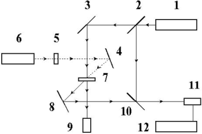
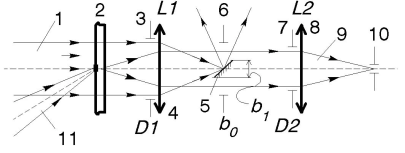
Presently, the two following schemes of LALS are developed. One of them — the conventional LALS or LALS with angular resolution — registers light scattered by all defects which are situated within the probe beam,2,10,12 see Fig.1. In the other — in scanning LALS microscopy or SLALS, which is a kind of the scanning laser microscopy,— every singular defects are visualized,17-20 see Fig.2. By combining these two schemes, one can determine concentration of defects, their spatial distribution, and hence, one can estimate the value of deviation of their dielectric constants from those of crystal bulk outside them (in the case of FCAs — and, as mentioned above, LSDAs always are FCAs,— the concentrations of free carriers in them, , can be evaluated).9,10,14,15
The LALS technique is of high sensitivity, it allows one to observe
defects with the variation of dielectric constant
down to 10-5–10-4 — i.e. with
down to 1013 cm-3. LALS is non-destructive and
contactless, it has no limitations on the tested wafer diameter.
INDUSTRIAL AND LABORATORY APPLICATIONS
Let us dwell on some possible specific applications of LALS as the
checking technique in the field of the industrial microelectronics.
Inspection of semiconductor wafer homogeneity
As mentioned above, LALS enables the observation of LSDAs with the sizes from several m to several tens m with point detect concentration in each of them down to 1013 cm-3. This method permits the investigation of the LSDA composition and the influence of various thermal treatments and operations of an industrial technological cycle on them. Wafer mapping is possible by means of SLALS. Incoming control with posterior utilization of substrates in the production process and technological step checking by using free chips are also possible.
These techniques are well developed now and a prototype of the instrument is available.
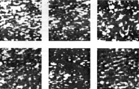
Fig.3 demonstrates the images of LSDAs in different bulk semiconductors obtained with the SLALS microscope (11 mm2 areas are presented). The microphotographs of LEC undoped InP , LEC InP:Fe , LEC SI GaAs annealed at 900∘C in a sealed quartz ampule when produced , CZ Si:B with high and low epd, and CZ Si:B coated with 1200 Å thick SiO2 layer are presented. White spots are the images of LSDAs. One can find more details on these pictures in Refs.[18-21].

The disadvantage of LALS (and SLALS) is its inability to
discriminate between LSDAs situated in crystal bulk and ones located
in near-surface layer. To remove this shortcoming, LALS tomography
with longitudinal resolution down to 10–20 m is now under development
on the basis of SLALS. The solution of the problem does not seem to meet any
difficulties. Its successful solving would enable the
testing of homogeneity of ”working” near-surface layers of wafers and
epitaxial layers. Note that layer inspection is possible even if it is
under coating or under other layer — up to the stage of metallization.
For instance, the homogeneity of a silicon wafer under
oxide layer may be checked — Fig.3— as well as
its near-surface layer .
Inspection of presence of LARDs in near-surface, near-interface and epitaxial layers
The methods of optical beam induced LALS (OLALS) and LALS with optical pumping,16 which may be used for such inspections, are the optical analogs of such well-known methods as EBIC and OBIC, yet they require neither Shottky barrier or junction nor complicated sample preparation. Like in the above case, a significant advantage of these techniques is their ability to test multilayer structures including layers covered with other layers. Also there are no limitations on sample size and resistivity in LALS. So wafer mapping, all-round incoming and step control with subsequent utilization of substrates in production cycle are possible.
Control of LSRDs in the substrate volume, including tomography, is also possible, but this is likely of interest for the production of -ray detectors, whose resolution is determined by LSDAs and LSRDs,10 various nuclear-ray counters, volume photodetectors, etc.
As of now, a cycle of experiments has been carried out, which have shown the possibilities of these methods.8,10,16,19,20

Fig.4 demonstrates the microphotographs of near-surface regions of
Si wafers subjected to different polishing and oxidation procedures
(11 mm2 areas are presented). The images of FZ Si:P
wafers after
chemico-dinamic and mechanical polishing procedures, and the
image of CZ Si:B wafer coated with 1200 Å thick SiO2
layer are given in this figure. The darker image, the shorter
non-equilibrium carrier effective lifetime is.
The focused 633-nm-wavelength radiation
of 55-mW He-Ne laser was used in this experiment for electron-hope pairs
photoexcitation in near-surface layers (see Fig.2).
Testing of specially doped areas
LALS may be also used for
the inspection of such parameters of specially doped domains of semiconductor
structures as their sizes, concentration of free carrier in them and
surface resistance. The inspection of these parameters is also
possible even after different layers are grown and coatings are given
(until metallized). The domains with the sizes greater than 1 m and
the variation of free carrier concentration greater than 1013
cm-3 can be tested.
Nowadays, the development of a prototype of such instrument is being
in the final stage.
Inspection of gettering process efficiency
We would like to specially emphasize that the above techniques might be very useful for the inspection of the gettering processes efficiency.22
The presence of the gettering precipitates at the internal gettering process can be checked by OLALS or LALS with quasi-bulk photoexcitation. The presence and parameters of impurity atmospheres around the gettering precipitates can be checked by the conventional (angle-resolved) LALS and SLALS microscopy. The ”working layer” may be tested by OLALS or LALS with surface photoexcitation.
The inspection of efficiency of the external gettering and gettering
by implanted
domains is also possible by the LALS-based techniques. The
procedures proposed for these inspections are analogous to those
described above for the internal gettering process.
CONCLUSION
So we can conclude that the LALS-based techniques might by a very
effective non-destructive tool for solving a wide class of problems of
materials and structures testing in modern microelectronics, which
might be used both in laboratories and directly in the production
cycle. We discussed only several most obvious possible
applications of these techniques in this paper. We are sure, however,
that they might find a great number of additional applications and be
useful in many branches of microelectronics science and industry.
REFERENCES
1. V.V. Voronkov, T.M. Murina, G.I. Voronkova
et al., Fiz. Tverd. Tela 20, 1365 (1978)
[Sov. Phys. Solid State 20 (5), 1365 (1978)].
2. V.V. Voronkov, G.I. Voronkova, B.V. Zubov et al.,
Fiz. Tverd. Tela 23 (1), 117 (1981)
[Sov. Phys. Solid State, 23 (1), 65 (1981)].
3. V.V. Voronkov, G.I. Voronkova, V.N. Golovina et al.,
J. Cryst. Growth 52, 939
(1981).
4. V.V. Voronkov, G.I. Voronkova, V.P. Kalinushkin et al.,
Fiz. Tekh. Poluprovodn. 18
(12), 2222 (1984)
[Sov. Phys. Semicond. 18 (12), 2222 (1984)].
5. S.E. Zabolotskii, V.P. Kalinushkin, T.M. Murina et al.,
Phys. Stat. Sol.(a) 88, 539
(1985).
6. N.V. Veselovskaya, V.V. Voronkov, G.I. Voronkova et al.,
Fiz. Tverd. Tela 27 (5), 1331
(1985)
[Sov. Phys. Solid State 27 (5), 1331 (1985)].
7. A.V. Voronkova, V.P. Kalinushkin, T.M. Murina, and N.S. Sysoyeva
Fiz. Tekh.
Poluprovodn. 19 (10), 1902 (1985)
[Sov. Phys. Semicond. 19 (10), 1902 (1985)].
8. V.P. Kalinushkin, D.I. Murin, T.M. Murina et al.,
Microelectronica 15 (6), 523 (1986)
[Sov. Phys. Microelectronics 15 (6), 523 (1986)].
9. S.E.Zabolotskii, V.P.Kalinushkin, D.I.Murin et al.,
Fiz. Tekh. Poluprovodn. 21 (8),
1364 (1987)
[Sov. Phys. Semicond. 21 (8), 1364 (1987)].
10. Victor P. Kalinushkin, in
Proc. Inst. Gen. Phys. Acad. Sci. USSR, Vol.4, Laser
Methods of Defect Investigations in Semiconductors and Dielectrics, edited by
A.A. Manenkov
(Nova, New York, 1988) pp. 1–75.
11. A.V. Batunina, V.V. Voronkov, G.I. Voronkova et al.,
Fiz. Tekh. Poluprovodn. 22 (7),
1308 (1988)
[Sov. Phys. Semicond. 22 (7), 1308 (1988)].
12. V.V. Voronkov, V.P. Kalinushkin, D.I. Murin et al.
J. Cryst. Growth 103, 126–130
(1990).
13. A.N. Buzynin, S.E. Zabolotskii, V.P. Kalinushkin et al.,
Fiz. Tekh. Poluprovodn. 24
(2), 264 (1990)
[Sov. Phys. Semicond. 24 (2), 264 (1990)].
14. V.P. Kalinushkin, V.A. Yuryev, and D.I. Murin,
Fiz. Tekh. Poluprovodn. 25, 798
(1991)
[Sov. Phys. Semicond. 25 (5), 798 (1991)].
15. V.P. Kalinushkin, V.A. Yuryev, D.I. Murin, and M.G. Ploppa, Semicond.
Sci.
Technol. 7, A255–A262 (1992).
16. V.P. Kalinushkin, D.I. Murin, V.A. Yuryev et al.,
in Second International
Symposium
on Advanced Laser Technologies, edited by V. Pustovoy and M. Jelínek, Proc. SPIE
2332, 146–153 (1994).
17. O.V. Astafiev, V.P. Kalinushkin, and V.A. Yuryev,
in Second International Symposium
on Advanced Laser Technologies, edited by V. Pustovoy and M. Jelínek, Proc. SPIE
2332, 138–145 (1994).
18. O.V. Astafiev, V.P. Kalinushkin, and V.A. Yuryev,
Mater. Sci. Eng. B (submitted for
publication).
19. V.P. Kalinushkin, V.A. Yuryev, and O.V. Astafiev,
presented at the First International
Conference on Materials for Microelectronics, Barcelona, Spain, October 18–23, 1994
(Mater. Sci. Technol, 1995) (submitted for
publication).
20. O.V. Astafiev, V.P. Kalinushkin, and V.A. Yuryev,
presented at the Ninth International
Conference on Microscopy of Semiconducting Materials, Oxford, UK, March 20–23, 1995
(IOP Conf. Ser.) (submitted for publication).
21. Vladimir A. Yuryev and Victor P. Kalinushkin, Mater. Sci. Eng. B
(in the press).
22. V.P. Kalinushkin, A.N. Buzynin, D.I. Murin, V.A. Yuryev,
O.V. Astafiev, and
A.I.Buvaltsev, presented at the First International Conference on Materials for
Microelectronics, Barcelona, Spain, October 18–23, 1994 (unpublished).