Recursive approach to study transport properties of atomic wire
Abstract
In this study, we propose a recursive approach to study the transport properties of atomic wires. It is based upon a real-space block-recursion technique with Landauer’s formula being used to express the conductance as a scattering problem. To illustrate the method, we have applied it on a model system described by a single band tight-binding Hamiltonian. Results of our calculation therefore may be compared with the reported results on Na-atom wire. Upon tuning the tight-binding parameters, we can distinctly identify the controlling parameters responsible to decide the width as well as the phase of odd-even oscillations in the conductance.
pacs:
73.63.-bElectronic transport in nanoscale materials and structures and 71.15.-mMethods of electronic structure calculation and 85.35.-pNanoelectronic devices1 Introduction
A mono-atomic quantum wire has a cross-section of one atom and is several atoms long. Such a system can be formed by pulling atomic contacts using a scanning tunneling microscope (STM) or a mechanically controllable break junction (MCBJ). The experimental evidences of formation of such atomic wires have been reported by Yanson et al 1 and Ohnishi et al add1 . However, issues involving electronic structure, transport properties and the influence of contacts with macroscopic conductors are still not fully settled. The most striking feature of such a mono-atomic wire is the non-monotonic behavior of its conductance as a function of the number of atoms along its length. Oscillatory behavior of conductance as a function of the length of the wire has been experimentally observed in Al, Pt and Ir wires by Smit et al 2 , in Au and Ag wires by Thijssen et al add2 , in Na wires by Krans et al ex1 and in wires of atoms of higher valency by Yanson et al 1 . This oscillatory behavior has been attributed to interference effect resulting from the changes in the connection between the wire and the edge of the electrode when new atoms are pulled into the wire.
Theoretically, the conductance of atomic wires can be calculated using the Landauer formalism in which one relates the conductance in the linear response regime to the transmittance at the Fermi energy, , as : . There are several numerical methods to calculate transmittance. They may be broadly classified into wavefunction and Green function methods. In wavefunction technique, one solves for scattering wavefunction of the system using methods like transfer matrix method huc1 ; huc2 ; trfm1 ; trfm2 ; trfm3 , finite difference method fdm or by solving Lippman-Schwinger equation lse1 ; lse2 . All these methods use various level of approximations to describe the electronic structure of the system, starting from semi-empirical models like extended Hückel huc1 ; huc2 to fully atomistic descriptions based on the density functional theory (DFT) of Kohn and Sham. In most of the wave function methods, however, the electronic structure of the scattering region is resolved in detail, while the leads are modeled by a free electron gas trfm1 ; trfm2 ; lse1 ; lse2 . Alternatively, conductance can be calculated by Green’s function method which does not require the explicit calculation of the scattering wave function. The main effort in this approach is to calculate the Green function of the central wire in the presence of the coupling to the leads. The effect of coupling to the leads is taken into account through self-energy terms. Various methods based on this approach, mainly differ in the choice of basis set used to represent the Hamiltonian and self-energy matrix, e.g Gaussians gs , numerical atomic orbitals lcao , wavelets wavelet and plane wave basis wannier . Although implementations within the Green function as well as the wavefunction approaches have been carried forward using various different techniques, it can be shown that the approaches are completely equivalent for non-interacting electrons10 . In this paper we propose a combination of the scalar and vector recursion techniques 26a ; 27 ; 26 as a viable and efficient means to study the transport properties within the general scheme of wavefunction approach of a lead-wire-lead system.
As a first step, starting from the junction point of the leads and the wire, we have used the recursion method of Haydock et al 26a ; 27 to map the quasi-1D semi-infinite leads with finite extensions along lateral directions onto equivalent chains. In the process, the information of the shape of the leads is encoded in the recursion coefficients. The recursion coefficients converge and the asymptotic part of the chains (or terminators) resembles periodic one-dimensional leads. This naturally divides the whole system unambiguously into an effective scattering region and two attached ballistic, periodic chain leads. The initial variation of the recursion coefficients contributes to the scattering region.
In the second step, the scattering matrix has been calculated by solving the Schrödinger equation using the vector or block recursion method of Godin and Haydock 26 and applying the wave-function matching conditions at the lead-wire interfaces.
In the final step, we have applied Landauer’s formula to express the conductance of the quantum wire.
The advantage of the proposed method is that it is a real space based method. Moreover, to solve the scattering problem, one does not need to calculate the wave function explicitly. By putting the boundary conditions at the lead-wire junctions and at the end of vector chain, one can directly calculate the scattering matrix. The basic inputs in the above described procedure are the tight-binding (TB) Hamiltonians for the wire and the leads. In order to illustrate the method we have applied it to a model system described by a single-band TB Hamiltonian. We demonstrate the validity of this approach by comparing the results obtained out of a simple model system with the reported results on monoatomic Na-wire calculated from first-principles. Moreover, by tuning the TB parameters of the wire and the leads we have provided a detailed understanding of the various features of the problem beyond what has been reported earlier 3 ; 5 ; 6 ; 7 ; 8 ; ex6 ; ex2 ; ex5 ; ex7 . The proposed technique being based on recursion, relies on the sparseness of the starting Hamiltonian. The coupling of this method to fully atomistic DFT description of the electronic structure, however, can be easily achieved in terms of Wannier function based Hamiltonian constructed out of DFT calculations.
2 Method
2.1 Converting quasi-1D lead to effective 1D chain and detection of effective scattering region
Each lead with finite lateral dimension of is described by a Hamiltonian in a tight-binding basis where labels a site and a particular channel, e.g. in a linear combination of atomic orbital (LCAO) type formulations, this would be the angular momentum labels :
| (1) |
where are the nearest neighbors of site on the lattice. To obtain the equivalent ‘chain’ or a tri-diagonal representation of the Hamiltonian, one needs to change the tight-binding basis to a new one : , obtained recursively.
Taking as the starting state, where 1 labels the site at the middle of the cross-sectional edge of the lead where it is connected to the wire (cf. Fig.1a) and is any one of the ‘orbital’ indices, we generate :
| (2) |
and
| (3) |
The equivalent Hamiltonian in this new basis is tri-diagonal (chain-like) :
| (4) |
where the index labels the ‘atoms’ of the equivalent linear chain for the channel and and signify its on-site and the hopping terms respectively. The sequences converge, so that for a given error tolerance , there exists an integer such that for and . The ‘terminator’ approximation puts for all . The initial ‘sites’ of both the equivalent input and output chain leads, therefore, contribute to the effective scattering region in addition to the wire. The wire of length 2 atoms is described by a Hamiltonian in the tight-binding basis as:
| (5) |
The opposite ends of the wire are coupled to the semi-infinite effective 1D leads via hopping matrix element . Note that as the starting state is same in the recursion process, the coupling coefficient remains same during the change of tight-binding basis set. The procedure therefore converts the whole system into an infinite linear chain in which effective scattering region is of extension sites and the rest represents the ballistic parts of the leads which do not participate in the scattering process.
2.2 Calculation of the scattering matrix
Let us consider and for convenience, rename the sites as follows (cf. Fig.1b) :
| (6) |
with
and
where and .
We then compute the scattering matrix of the above mentioned system using the block or vector recursion technique introduced by Godin and Haydock 26 . The essence of the vector recursion technique is the block tridiagonalization of the system Hamiltonian by changing to a new orthogonal set of vector basis, with the restriction that the ballistic part of effective 1D lead Hamiltonian remains unchanged. In this last aspect, it differs from the standard Lanczos method 27 . The numerical stability of this method 30 has been established in studying problems related to Anderson localization and quantum percolation model 31 and layering transition in 2D nano-strip 29 previously. Below we describe the method briefly.
Let us consider, for the sake of demonstration, that we have two 1D ballistic leads, one incoming and and another outgoing connected to the opposite ends of the scattering region at positions and (cf. Fig.1b). The leads and the scatterer have scattering channels. The member of the new basis are generated by clubbing the input and output leads together as the vector lead and so is the scattering region (cf. Fig.1c). The lead states are chosen to be
| (9) |
with and = . The starting state within the scattering region is chosen to be
The subsequent members of the basis are generated from
| (11) |
The matrix inner product is defined as the matrix
where the matrices and are :
If this matrix is then the states are called orthogonal.
It can be shown that the matrices and are block-tridiagonal members of the matrix representation of the Hamiltonian in the new basis:
| (12) |
so that the transformed Hamiltonian matrix can be divided in blocks, with only non-zero diagonal and sub-diagonal blocks.
The wave function may be represented in this new basis by
a set so that
= . These wave function amplitudes also satisfy an equation
identical with (11).
In the ballistic part of the effective 1D lead chain, the onsite and hopping terms do not vary. Therefore, electron potential must be periodic in this region and the solution to the Schrödinger’s equation in the channel of the ballistic leads are traveling Bloch waves : . As the wave travels in the leads, the phase of its wave function changes by , where is the energy of the incoming electron. In order to have only propagating solutions, we fix E as real and . This sets the energy window. This is reasonable because eventually only the propagating modes enter in the expression of transmission matrix elements, as evanescent modes do not contribute to the transmission directly. In the channel of the incoming lead, the incident and the reflected waves can be expressed as a sum
The second term is the reflected wave in the channel from incident waves in channels.
In the channel of the output lead there is a transmitted wave from incident waves in channels 33
and are the complex reflection and transmission coefficients. The boundary conditions are then imposed from the known solution in the leads at the junction labeled by 0 and 1:
| (15) |
| (18) |
The amplitude at the -th basis may be written as
| (19) |
where and satisfy the same recurrence relation as (11) with replacing and also satisfy the boundary conditions = and = , while = and = . Note that and are matrices and ’s are column matrices of dimension 2.
This new basis terminates after = steps, as the rank of the space spanned by the original tight-binding basis remains unchanged after the transformation. Hence the recursion also terminates after steps. This gives an additional boundary condition,
| (20) |
If we now interchange the incoming and outgoing leads, we get a similar pair of equations for and , the transmission and reflection coefficients for a wave incident from the second lead. Time-reversal symmetry demands that must be the same for waves of the same energy incident from either lead so that = In addition, and differ only by a phase factor. Solving these equations for the S-matrix in the effective scattering region, one has,
| (23) | |||||
where
The various steps of our approach are shown schematically in Fig. 1.

The conductance is then given by Landauer formalism. It expresses the electronic conductance in one-dimensional conductor as a quantum mechanical scattering problem and relates to the total transmission probability of the electron at the Fermi level32 , T(), as
| (24) |
We have assumed in our derivation the leads to have finite lateral dimensions, though in actual experiments, the leads are three dimensional. In order to study the influence of the extend of the lateral dimension of the leads, we have checked our results with increasing size of the lateral cross-section of the leads. Though the quantitative values do change with the change of the lateral dimension, the qualitative nature holds good in every case. In addition, we find for sufficiently large choice of lateral cross-section, the recursion coefficients (, ) for the leads converge to that of a bulk system (see for details section 3.1), indicating for such large lateral cross-section, the leads behave as truly three-dimensional leads. The other approach to the problem could have been inclusion of periodic boundary condition as have been adopted in various works lcao ; wavelet ; wannier ; 10 ; pbc1 ; pbc2 ; pbc3 . If we impose periodic boundary conditions on the lead surfaces, only those modes which are consistent with the boundary conditions can travel through them. In an earlier paper we have shown mtm , that it is possible to change over from a site to a mode basis and reformulate the vector recursion in the new basis. The lead is broken up into slices perpendicular to its length and the composite site label is partitioned into two : one is the slice label and the other is the position on this slice . The basis is then converted into a slice-mode basis and the Hamiltonian is expressed in this new basis. Exactly as the Hamiltonian (6) mixes orbital labeled channels because of off-diagonal terms , in the mode based formalism off-diagonal terms in the corresponding Hamiltonian causes the outgoing wave to be of a mixed mode type even if the incoming wave is in a single mode. Otherwise, the formal methodology is identical in the two cases. The interested reader is referred to the paper referenced above for the details.
3 Application
3.1 The model
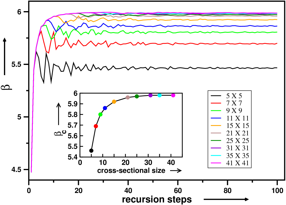
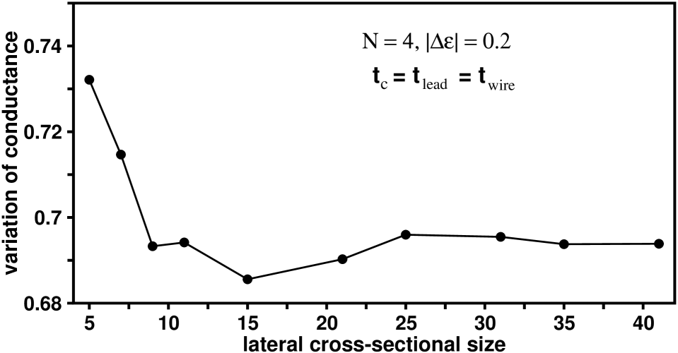
Since our aim here is to propose a method rather than to evaluate the properties of any particular system in quantitative detail, we present the study of a simple model system. It consists of a wire, few atoms long, sandwiched between two identical semi-infinite leads. Both the wire and the leads have only a single channel ( corresponding to single -band. The cross-sectional size of each lead in our calculation was 55. The atoms in the leads form a simple cubic lattice. Each lead is described by a single-band nearest-neighbor TB Hamiltonian. Two TB parameters in equation (1) : the on-site and the hopping terms, which are material specific in realistic cases, have been chosen as = = 0 and = = 2 in some arbitrary energy unit. As a first step, we performed scalar recursion on the leads to convert them into equivalent chains and determined the contribution of each lead to the effective scattering region. We took the starting state of recursion to be the sites which bound the leads to the wire. For a simple cubic lead, the recursion coefficients = 0 while the other coefficients fluctuate with recursion steps converging to an asymptotic value . The convergence of depends on the lattice structure and lateral cross-sectional size of lead. We have not used any periodic boundary conditions in the lateral direction. To see the finite size effect of lead in the lateral direction, we have repeated our calculations for different cross-sectional sizes. Convergence of with recursion steps for different cross-sectional sizes is shown in Fig.2. As the cross-section increases, the number of recursion steps required to converge decreases (i.e size of effective scattering region decreases which facilitates to easier computational execution). Variation of converged value () with lateral cross-sectional size of the lead is shown within the inset. Notice after a certain cross-sectional size (30 30 with the present choice of parameters), converges to that of the bulk cubic system, which is 6 for choice of = 0 and = 2.0. This implies that there is no further effect of finite cross-section on and therefore on conductance. In changing cross-section from 55 to 3030, changes by 9 % (The change is mostly coming in going from 55 to 1111 and after that change is very minute). The corresponding change in conductance is much smaller : 5 % for even numbered wire, less than 1 % for odd numbered wire (cf. Fig. 3). We have checked that qualitatively results are same for any cross-sectional size, but if one is concerned about the quantitative value, then convergence of with cross-sectional size has to be checked. For our chosen case, converged after around 80 recursions. So in our calculation, was taken to be 80 and for . For a model simple cubic lead, the Fermi energy is at = which is obvious from the dispersion relation for a half-filled band with Fermi wave number = . Fermi energy of the lead-wire-lead system tends to align with the Fermi energy of the semi-infinite lead. Conductance is therefore calculated at = .
3.2 Results and discussions
Our calculated conductance as a function of number of atoms in the wire is shown in Fig.4. The inter-atomic hopping within the wire was fixed to = 2 = . To consider the effect of charge transfer between the leads and the wire [ = - 0], we considered the cases = 0.2 and = 0.4 along with no charge transfer condition = 0. Non zero values of were achieved by changing . For each case, we considered three types of coupling between lead and atomic wire, given by lead-wire hopping coefficient : (i) = 0.9 for weak coupling, (ii) = for direct coupling and (iii) = 1.1 for strong coupling.
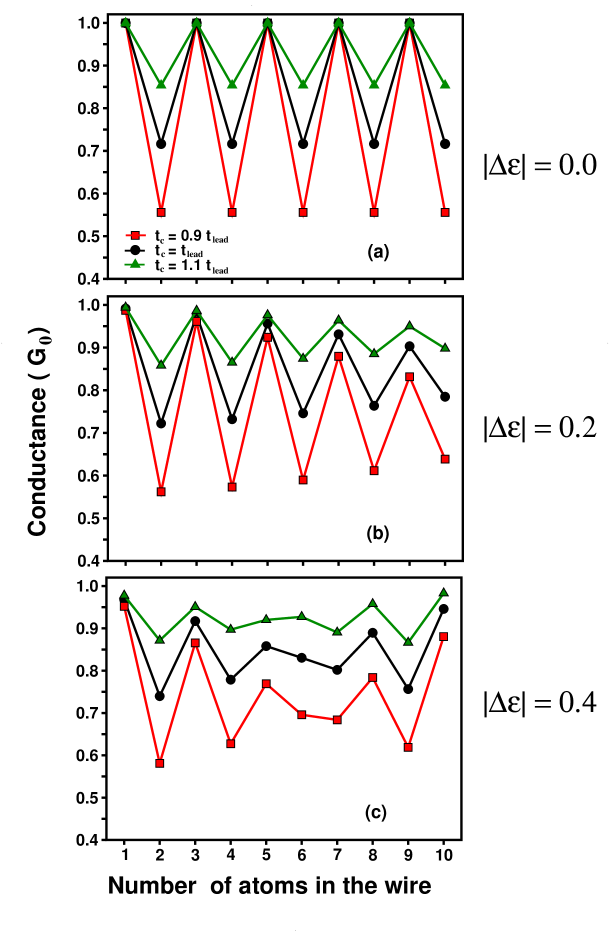
The odd-even oscillation in conductance for no charge transfer situation is obvious from Fig.4a i.e wires with odd-number of atoms have larger conductance as compared to the even numbered ones, for all the three types of couplings. In this ideal case of no charge transfer situation, all odd numbered atomic wires have conductances equal to quantum unit = for all the three coupling cases, while for even numbered wires the conductances are lower. The conductance of even-numbered wires decreases as one moves from strong to direct to weak coupling. This means that the amplitude of conductance oscillation is a maximum for the weak coupling case ( = 0.9 ) and it is a minimum for the strong coupling case ( = 1.1 ). Similar results have been predicted by Khomyakov et al for a system of 1D wire connected with 1D leads using tight-binding calculation 8 . The dependence of conductance on for even numbered wire is given by
It follows the same trend as observed in the top panel of Fig.4. Another point to notice from Fig.4a is that the length of the wire does not have any effect in this case either on amplitude or phase of the oscillation. All odd numbered atomic wires and also all even numbered atomic wires have equal conductances for a fixed coupling type. The odd-even oscillations for our single band model system is in agreement with the results on Na-atom wires3 ; 5 ; 6 ; 7 ; 8 ; ex6 ; ex2 .
For = 0.2 in Fig.4b, the odd-even oscillation in conductance is again obvious within the range of our plot. However, a close view to these curves, indicates that the conductance of the odd numbered atomic wires gradually decreases while that of the even numbered atomic wires slowly increases. If we increase the number of atoms in the wire to more than 10 (not shown in Fig.4), we find that the parity of conductance oscillation changes from odd-even to even-odd, i.e even numbered atomic wires now have larger conductance than the conductance of odd numbered atomic wires.
Increasing to 0.4, there will be larger charge transfer between the lead and wire. This causes a change in the parity of conductance oscillation from odd-even to even-odd for even shorter lengths : around wire lengths of 7 atoms as shown in Fig.4c. From our study, it is therefore clear that the amplitude of conductance oscillation is mainly controlled by coupling coefficient between the leads and the wire, while the parity of the oscillation is controlled by the length of the wire and onsite energy difference between wire and lead Hamiltonians. There are few reports ex6 ; ex5 which indicate the change of parity of conductance oscillation and variation of oscillation amplitude for Na-atom wire.
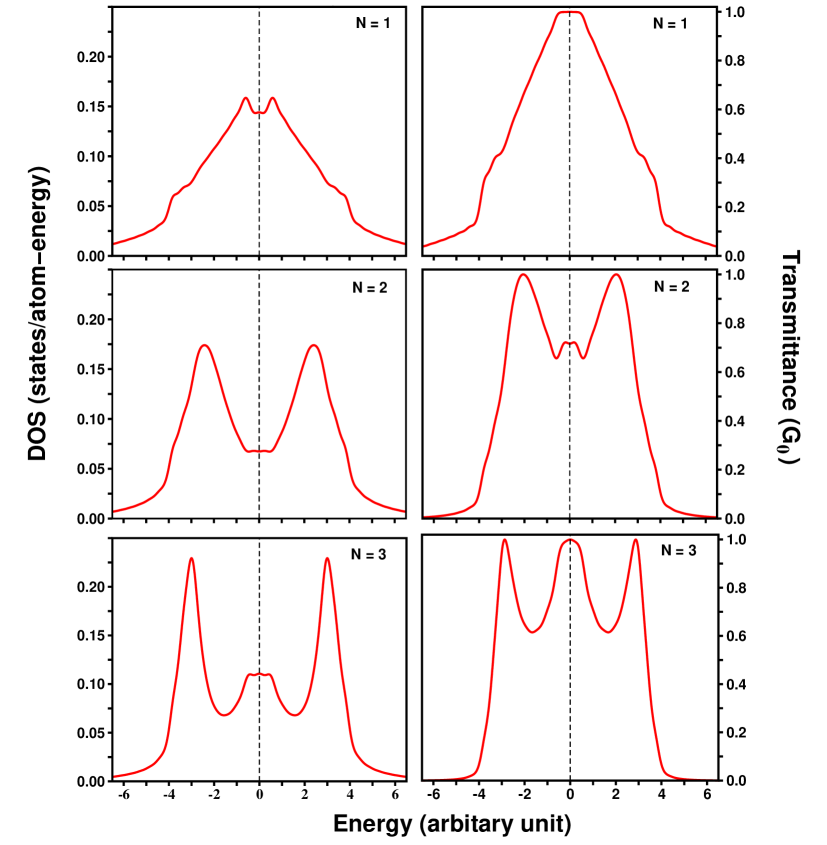
To understand the odd-even oscillation in the conductance, we have calculated the density of states (DOS) and transmittance as a function of energy for wires of lengths = 1, = 2 and = 3 for the case of zero charge transfer. The results shown in Fig.5 bring out the essential mechanism which has been discussed also in ref. 8 . For odd-numbered atomic wires, the Fermi-energy falls in the non-bonding peak and it gives a maximum in the transmittance at = . On the other hand, for even numbered wire, the Fermi level lies in the minimum between the bonding and non-bonding peaks and consequently it exhibits a less transmission at = .
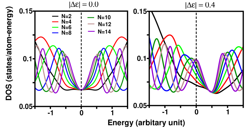
In order to explain the flipping of conductance oscillation from odd-even to even-odd, we have plotted in Fig.6 the DOS around Fermi energy of several even numbered atomic wires for two cases of no charge transfer and finite charge transfer situations. When there is no charge transfer ( = 0), all the even numbered wires have a minimum in DOS at . When we allow sufficient charge transfer to take place between wire and lead, DOS at gradually increases with increasing length and at a critical size, a peak will appear in DOS at . The opposite occurs for odd-numbered atomic wire (not shown in the Fig.6) and nature of conductance oscillations flips from odd-even to even-odd. If we increase the wire size further, again after another critical size, the odd-even nature of oscillations is restored. This repetition of even-odd or odd-even oscillation continues with increasing wire size.
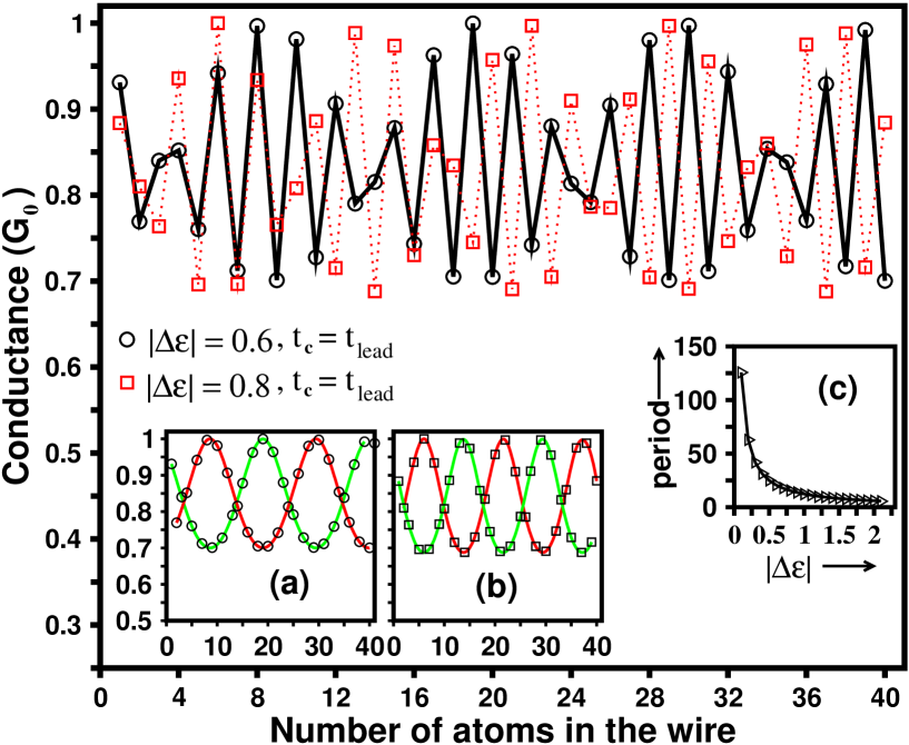
To investigate the effect of on the period of parity flip, we have plotted the conductance as a function of number of atoms in the wires in Fig.7 for two different values of keeping coupling parameter fixed. One can see clearly that as increases, frequency of parity flip increases i.e period of parity flip decreases. To get a better insight into parity flip, we have shown in Fig.7 the conductance variation of odd numbered and even numbered wires separately in insets (a) and (b) for = 0.6 and = 0.8 respectively. Each curve shows sinusoidal-like variations. Curves of even numbered and odd numbered wires together constitute loops. Length of one loop indicates the wire size required to flip the oscillation from odd-even to even-odd. The nodal points of loop indicate the boundaries between odd-even and even-odd. Two consecutive loops constitute a period. Number of loops in inset (b) is larger than in inset (a). Variation of period of parity-flip with is shown by right triangles in inset (c). For = 0, there is no parity flip i.e period is infinity. As increases, the period decreases. For sufficiently large value of (), odd-even nature of conductance oscillation no longer persists. Period of conductance oscillation then changes to more than two atoms which is the characteristic of wires consisting of atoms of higher valency. Within the odd-even nature of conductance oscillations, the period of parity flip goes roughly as with = 12.605 and = -0.253.
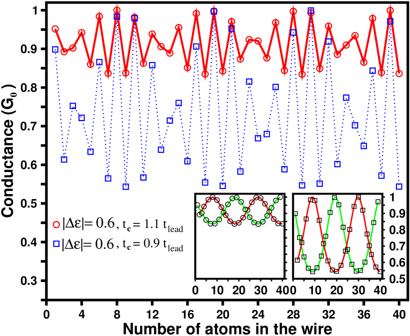
However, coupling parameter does not have any effect on period of parity flip. To check this, we have plotted the conductance variation with wire size in Fig.8 for two different coupling constant keeping fixed, while insets (a) and (b) show the conductance variation of odd numbered wires and even numbered wires separately. The number of loops in both the cases are same indicating has no effect on the period. Larger width of loops in inset (b) compared to that in inset (a) indicates that controls the amplitude of odd-even oscillations .
| wire length | tc1 = tlead | tc1 = tlead | tc1 = tlead |
|---|---|---|---|
| (N) | tc2 = tlead | tc2 = 1.1 tlead | tc2 = 1.2 tlead |
| 1 | 0.9996 | 0.9906 | 0.9672 |
| 2 | 0.7164 | 0.7876 | 0.8482 |
| 3 | 0.9996 | 0.9906 | 0.9672 |
| 4 | 0.7164 | 0.7876 | 0.8482 |
| 5 | 0.9996 | 0.9906 | 0.9672 |
So far we have studied the role of the charge neutrality on the conductance oscillations of monoatomic wires considering the mirror symmetry between the two junctions. We found odd-even oscillation in the conductance. Moreover, for no charge transfer situation, conductance of odd numbered wires is quantized to , while for even numbered wires conductance is less than . Now we consider the situation where mirror symmetry between two lead-wire junctions is broken by using two different coupling coefficients for two junctions, keeping charge-neutrality intact. Table 1 contains our result. Clearly, odd-even oscillations still occur, but the conductance quantization for odd numbered wires is weakened by reducing the value less than . This observation is in accordance with the previous study6 ; mirror .
To conclude, we have used combination of real-space based scalar and vector recursion techniques to study the transport properties of a lead-wire-lead system. Our study on model system described by single band TB Hamiltonian provides a detail understanding of the effect of lead-wire coupling on the conductance of monoatomic wire. Working with model system, gives us the freedom of changing the model parameters and allows us to work with much longer wires than usually considered in liturature. Odd-even oscillation in the conductance with increasing length of wire has been observed in agreement with earlier studies 3 ; 5 ; 6 ; 7 ; 8 ; ex6 ; ex2 ; ex5 ; ex7 . In presence of charge neutrality between the leads and the wire and in presence of perfect mirror symmetry between the incoming and outgoing leads, the conductance of odd numbered wires is quantized to , while it is less than for even numbered wires. As the charge neutrality is broken, the oscillation in conductance still exists, but with the distinction that for a given choice of charge transfer () and lead-wire hopping (), the conductance values of the odd numbered and even numbered wires are no longer fixed quantities as the size of the wires is changed. For such systems, we further found a change of phase of conductance oscillation from odd-even to even-odd with increasing number of atoms in the wire. We found that while the amplitude of oscillation depends on lead-wire coupling parameter , it is the amount of charge transfer between lead and wire, which affects the period of oscillation. Lifting of mirror symmetry between two lead-wire junctions in no charge transfer condition is found to reduce the conductance of odd numbered wires below the quantized value of . The proposed technique can be easily generalized for application to realistic cases. To apply this approach to real systems, one needs to generate TB parameters of lead and wire via self consistent calculations while multi-orbital effect can be taken into account via multi-channel generalization of Landauer-Büttiker formula (see equation 24). The proposed real space technique of calculation of conductance coupled with localized Wannier basis generated out of self-consistent DFT calculation wannier1 ; wannier2 can lead to a viable technique for study of quantum transmittance and conductance of nanoscale systems of various geometries in general. Work is in progress along this direction.
S.D thanks Council of Scientific and Industrial Research (Government of India) for financial support and TSD acknowledges Department of Science and Technology (Government of India) for support through Swarnajayanti fellowship.
References
- (1) A. I. Yanson, G. R. Bollinger, H. E. van der Brom, N. Agrait, J. M. van Ruitenbeek, Nature 395, 1998 783
- (2) H. Ohnishi, Y. Kondo, K. Takayanagi, Nature 395, (1998) 780
- (3) R. H. M. Smit, C. Untiedt, G. Rubio-Bollinger, R. C. Segers, J. M. van Ruitenbeek, Phys. Rev. Lett. 91, (2003) 076805
- (4) W. H. A. Thijssen, D. Marjenburgh, R. H. Bremmer, J. M. van Ruitenbeek, Phys. Rev. Lett. 96, (2006) 026806
- (5) J. M. Krans, J. M. van Ruitenbeek, V. V. Fisun, I. K. Yanson, L. J. de Jongh, Nature (London) 375, (1995) 767; A. I. Yanson, I. K. Yanson, J. M. van Ruitenbeek, ibid. 400 (1999) 144
- (6) P. Sautet, C. Joachim, Phys. Rev. B 38, (1988) 12238
- (7) E. G. Emberly, G. Kirzenow, Phys. Rev. B 58, (1988) 10911
- (8) K. Hirose, M. Tsukada, Phys. Rev. Lett. 73, (1994) 150
- (9) K. Hirose, M. Tsukada, Phys. Rev. B 51, (1995) 5278
- (10) H. J. Choi, J. Ihm, Phys. Rev. B 59, (1999) 2267
- (11) P. A. Khomyakov, G. Brocks, Phys. Rev. B 70, (2004) 195402
- (12) N. D. Lang, Phys. Rev. B 52, (1995) 5335; N. D. Lang, Phys. Rev. Lett. 79, (1997) 1357
- (13) M. D. Ventra, S. T. Pantelides, N. D. Lang, Phys. Rev. Lett. 84, (2000) 979
- (14) Y. Xue, S. Datta, M. A. Ratner, Chem. Phys. 281, (2001) 151
- (15) M. Brandbyge, J. L. Mozos, P. Ordejon, J. Taylor, K. Stokbro, Phys. Rev. B 65, (2002) 165401
- (16) K. S. Thygesen, M. V. Bollinger, K. W. Jacobsen, Phys. Rev. B 67, (2003) 115404
- (17) A. Calzolari, N. Marzari, I. Souza, M.B. Nardelli, Phys. Rev. B 69, (2004) 035108
- (18) P. Khomyakov, G. Brocks, V. Karpan, M. Zwierzycki, P. J. Kelly, Phys. Rev. B 72, (2005) 035450
- (19) R. Haydock, V. Heine, M. J. Kelly, J. Phys. C :Solid State Phys 5, (1972) 2845
- (20) R. Haydock, Solid State Physics, editor: H. Ehrenreich, F. Sietz, D. Turnbull (Academic, New York, 1980) volume 35
- (21) T. J. Godin, R. Haydock, Phys. Rev. B 38, (1988) 5237
- (22) T. J. Godin, R. Haydock, Comp. Phys. Comm. 64, (1991) 123
- (23) I. Dasgupta, T. Saha, A. Mookerjee, Phys. Rev. B 47, (1993) 3097
- (24) S. Datta, D. Choidhuri, T. Saha-Dasgupta, S. Sengupta, Eup. Phys. Lett. 73, (2006) 765
- (25) The process of vector recursion converts the lattice into a one-dimensional chain, which is then folded to clump two sites of the chain together to define the vector basis set . For a chain with folded configuration (see Ref. 26 for details) both the reflected and transmitted waves move in the opposite direction to that of the incident wave.
- (26) The Fermi energy of the lead-wire composite system is determined by the macroscopic lead Hamiltonian.
- (27) M. B. Nardelli, Phys. Rev. B 60, (1999) 7828
- (28) K. S. Thygesen, K. W. Jacobsen, Chem. Phys. 319, (2005) 111
- (29) P. A. Khomyakov and G. Brocks, Phys. Rev. B 70, (2004) 195402; K. Xia, M. Zwierzycki, M. Talanana and P. J. Kelly, Phys. Rev. B 73, (2006) 064420
- (30) K. Tarafder, T. Mitra and A. Mookerjee, Physica B 371, (2006) 100
- (31) N. D. Lang, Phys. Rev. Lett. 79, (1997) 1357
- (32) S. Tsukamoto, K. Hirose, Phys. Rev. B 66, (2002) 161402
- (33) H. -S. Sim, H. -W. Lee, K. J. Chang, Phys. Rev. Lett. 87, (2001) 096803
- (34) P. Havu, T. Torsti, M. J. Puska, R. M. Nieminen, Phys. Rev. B 66, (2002) 075401
- (35) P. Khomyakov, G. Brocks, Phys. Rev. B 74, (2006) 165416
- (36) R. Gutierrez, F. Grossmann, R. Schmidt, Acta Phys. Pol. B 32, (2001) 443
- (37) Y. Egami, T. Ono, K. Hirose, Phys. Rev. B 72, (2005) 125318
- (38) P. Major, V. G. Suarez, S. Sirichantaropass, J. Cserti, C. J. Lambert, J. Ferrer, G. Tichy, Phys. Rev. B 73 (2006) 045421
- (39) J. K. Viljas, J. C. Cuevas, F. Pauly, M. Hafner, Phys. Rev. B 72, (2005) 245415
- (40) H. -W. Lee and C. S. Kim, Phys. Rev. B 63, (2001) 075306
- (41) N. Marzari, D. Vanderbilt, Phys. Rev. B 56, (1997) 12847
- (42) O. K. Andersen, T. Saha-Dasgupta, Phys. Rev. B 62, (2000) R16219