Mid-IR-laser microscopy as a tool for defect
investigation in bulk semiconductors
O V Astaf iev, V P Kalinushkin and V A Yuryev
General Physics Institute of RAS, 38, Vavilov Street, Moscow,
117942, Russia
ABSTRACT:
A non-destructive optical technique described in
this paper is an effective new tool for the investigation of
defects in semiconductors. The basic instrument for this
technique — a mid-IR-laser microscope — being sensitive to
accumulations of free carriers enables the study of both
accumulations of electrically-active defects or impurities in
bulk semiconductors and doped domains in semiconductor
structures. The optical beam induced scattering mode of this
microscope is designed for the investigation of recombination-active
defects but unlike EBIC it requires neither Schottky barrier or
– junction nor special preparation of samples.
1. INTRODUCTION
At present, many techniques have been developed to study defects on the micron and sub-micron scale in semiconductors. Unfortunately most of them either break down the studied sample or require rather complicated procedures of sample preparation that in some cases may modify the properties of the defects studied. Moreover, practically all of the modern methods for investigating such defects enable at best to observe defects but cannot give information about their composition. The specificity of the techniques which may be applicable for analysis of defect composition, such as e.g. X-ray microanalysis, microcathodoluminescence or photoluminescence, does not allow one to investigate defects situated in crystal bulk. Even the defects located in near-surface regions are hard to be studied by these methods because of insufficient sensitivity or, like in the case of X-ray microanalysis, because the defects are often composed of intrinsic defects. So despite the great success that now has been achieved in the understanding of defect formation mechanisms, their composition and properties, new methods for defect investigations, which might appreciably accelerate the progress in these issues, are presently required like they never were in the past. Non-destructive methods for investigation of defects in crystal bulk might e.g. give opportunities for direct studies of the processes of inner gettering especially if they are combined with techniques for studies of defects located in near-surface layers. Considerable progress may be achieved in the investigation of defects located in the vicinity of semiconductor interfaces and surfaces coated with dielectric layers and so on. We could give many examples of other applications of such techniques (see e.g. Kalinushkin et al 1995b). From our viewpoint, the most attractive methods for such investigations are those which enables the study of the crystal domains enriched with electrically-active defects and/or defects interacting with non-equilibrium carriers (we call them large-scale electrically-active defect accumulations, LSDAs, and large-scale recombination-active defects, LSRDs). The most appropriate methods for investigating these defects are those sensitive directly to micron-scale variations of the free carrier concentration. This is because many of the procedures for determining the point-defect structure of materials, e.g. such as measurements of temperature dependencies of conductivity or photocurrent measurements, may be suited for these techniques.
It seems, however, that until recently, the low-angle mid-IR-laser light scattering technique, LALS (see Kalinushkin 1988, Voronkov et al 1990, Kalinushkin et al 1995b and many references therein), was the only method that satisfied all these requirements, and many studies of LSDAs and LSRDs in different materials were carried out by this method — see e.g. references cited by Kalinushkin et al (1995b) and Kalinushkin (1988). Nonetheless LALS in its standard form (or LALS with angular resolution) has two main disadvantages: firstly, it does not permit the study of each individual defect and gives information averaged over a group of defects with close parameters which are located within the probe beam, and secondly, using only LALS one cannot estimate the concentrations of LSDAs which are necessary to evaluate such parameters as free carrier concentrations in LSDAs (and, hence, the energy locations of point centers constituting them). Therefore one must use other methods to evaluate the concentrations of LSDAs which decreases the reliability of the information obtained (however, the data obtained e.g. by Kalinushkin et al (1991) for InP and GaAs were confirmed by Yuryev and Kalinushkin (1995) and Yuryev et al (1995) by direct observations).
To overcome the mentioned shortcomings of LALS, a new method for visualization of free carrier accumulations was recently proposed (Astafiev et al 1994b, Kalinushkin et al 1995b, Astafiev et al 1995a, Astafiev et al 1995b and Yuryev et al 1995), which is a kind of scanning laser microscopy working in the mid-infrared wavelength range. Being an evolution of LALS (it is often referred to as scanning LALS or SLALS), this method possesses all its merits and admits all modifications which make LALS so convenient for investigation of LSDAs. Before long, the optical beam induced LALS (OLALS) mode of the mid-IR-laser microscopy was developed (Astafiev et al 1995c, Astafiev et al 1995d and Kalinushkin et al 1995b) on the basis of LALS with surface photoexcitation (Kalinushkin et al 1994a and Kalinushkin et al 1995a) for investigation of LSRDs in near-surface and near-interface layers of semiconductors. The latter technique is a non-destructive contactless optical analog of EBIC or, more exactly, OBIC but in contrast to these methods OLALS does not require Schottky barrier or – junction and any special surface preparation.
The present paper is devoted to the description of the
developed techniques of mid-IR-laser microscopy and illustration
of their serviceability by the experimental results obtained for
bulk Si single crystals and their near-surface regions.
2. SLALS MODE OF MID-IR-LASER MICROSCOPE
2.1 Basic Instrument
The SLALS technique is shown schematically in Fig.1. The plane wave of the laser source illuminates a thin semiconductor parallel-sided crystal with polished surfaces (usually standard technological wafer before structure production). The wafer is located in the focal plane of a lens L1. Let a defect be in the crystal bulk in the front focal plane of L1. It scatters the probe wave producing an additional scattered wave, which diverges in an angle of an order of where is the wave-length, a is the defect’s characteristic size. A resultant wave after the defect is the sum of the undisturbed plane wave and that scattered by the defect. The lens L1 condenses the plane wave in the back focus to a spot with the size of about where is the diameter of the probe plane-wave beam, is the focal length of the lens L1. A small mirror turned to the angle of 45∘ to the focal plane or an absorbing screen is positioned in the back focal plane to remove the probe wave radiation. The scattered wave, being almost a plane wave with characteristic beam diameter of after L1, passes to the second lens L2 almost without losses if the screen size is smaller than . So the scattered wave without probe radiation reaches the lens L2 and the image of the defect is formed in the back focal plane of L2 in scattered rays.
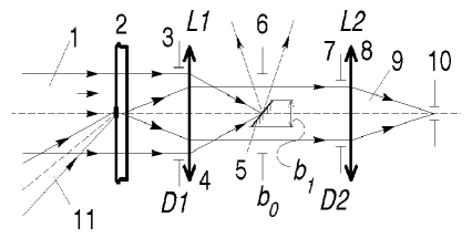
The detailed analysis of the SLALS technique with application
to the the central dark field method of spatial-frequency signal
filtering, which is schematically presented in Fig.1, is made in
the paper by Astafiev et al (1995b).
2.2 LSDAs in CZ Si:B
The single crystals of standard industrial Si:B studied in this work were grown by the Czochralski (CZ) process and had the specific resistivity of 12 cm. The thickness of the samples was 300 m. The large-scale electrically active defects with the dimensions ranging from 3–5 m to 40–50 m were observed previously in analogous crystals in the works by Buzynin et al (1990) and Astafiev et al (1994a). Their concentrations were estimated as 105–107 cm-3, the values of the relative variations of the dielectric constants in them were evaluated as 10-3–10-4.
The specimens sharply differing in the concentration of defects as determined by selective etching were studied in the present work: their concentrations were about 2105 cm-3 in the sample 1 and about 2104 cm-3 in the sample 2.
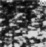
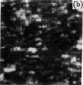
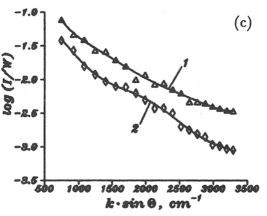
Fig.2 presents the microphotographs of these samples obtained with the use of SLALS (the areas of 11mm2 are depicted in the photographs). Like in the photographs of indium phosphide and gallium arsenide (Yuryev and Kalinushkin 1995), the white spots in the pictures are the images of LSDAs. The mean value of the light scattering intensity by the defects in Fig.2 is by around 3 times greater than that in Fig.2, that is completely in agreement with the results obtained by LALS — the ratio of the light scattering intensities by the samples 1 and 2 in the LALS diagrams given in Fig.2 is also nearly equal to 3. The concentration of defects determined in the sample 1 was about 106 cm-3, whereas that in the sample 2 was about (4–5)105 cm-3.
Note that the values of the defect concentrations revealed in the analogous samples by EBIC with the special surface preparation (Buzynin et al 1989) appeared to be nearly equal to the above values obtained by SLALS.
The results obtained allow us to conclude the following: 1) using the SLALS-microscope we visualized the defects which were previously investigated by LALS — the so called ”weak impurity accumulations” (Buzynin et al 1990 and Astafiev et al 1994a); 2) using EBIC with the special surface preparation — the data obtained by this method were used by Buzynin et al (1990) and Astafiev et al (1994a) — we also revealed namely ”weak impurity accumulations”, i.e. the estimations of LSDAs parameters and thermal activation energies of the centers constituting LSDAs made by Buzynin et al (1990) and Astafiev et al (1994a) are valid.
The radii of the accumulations calculated from the LALS diagrams given in Fig.2 are m. Measuring the zero-angle light scattering intensity I0/W from LALS and determining the concentration of LSDAs from SLALS one can easily estimate the values of in LSDAs. They are (6.5–10)10-4 and (11–14)10-4 for the samples 1 and 2, respectively.
Note also that the correlation between the concentrations of defects
revealed by selective etching and SLALS is purely qualitative. This is
also characteristic for most of the comparative experiments on
etching and LALS. However, enquiring into the reasons for the
discrepancies observed is beyond the scope of this paper.
3. OPTICAL BEAM INDUCED LALS
3.1 Description of the Method
This mode of SLALS was recently proposed by us (Kalinushkin et al 1995b and Astafiev et al 1995c, 1995d) as a scanning modification of LALS with sample photoexcitation (Kalinushkin 1988, Kalinushkin et al 1994 and Kalinushkin et al 1995a). Its principle diagram is given in Fig.1. The method, as well as LALS, can work in two modes: in the mode of bulk photoexcitation and in the mode of surface photoexcitation. The regimes are different only by the choice of pumping laser: the first regime uses a laser with quantum energy less than the studied sample bandgap, whereas the second one uses a laser with quantum energy greater than the bandgap, and in general both regimes are quite analogous.
The essence of the method, say for surface excitation, is as follows. A highly focused beam (in contrast to LALS with photoexcitation where a wide beam is used) generates electron-hole pairs in the sample (in the chosen case, in its near-surface region). If the characteristic dimensions of the non-uniformity of the generated electron-hole pair distribution are as small as it is required in the paper by Astafiev et al (1995b), the scattered mid-IR-laser light of the SLALS microscope starts reaching the photodetector. Its intensity is proportional to the square of generated carrier concentration in the spot. The characteristic sizes of the non-uniformity are controlled by the sizes of the exciting laser spot, the carrier diffusion length and the surface recombination velocity. Even if the diffusion length is large (e.g. in Si), the inhomogeneity with small enough characteristic dimensions remains in the carrier distribution because of the surface recombination. This inhomogeneity is detected by the SLALS microscope. The carrier concentration in such a ”droplet” is controlled with the electron-hole pair life-time in a given area of the sample.
It is clear that the method is a very close analog of the electron or optical beam induced current (EBIC or OBIC) methods, but is different in that OLALS requires neither a Schottky barrier nor a – junction. It also does not require any special preparation of surfaces.
But the most important property of the developed method is its ability to obtain information from interfaces and surfaces covered with coatings and epilayers until the wafer is metallized.
It is also possible to create a kind of tomographic microscopy on the basis of OLALS, and this problem does not seem to be very difficult.
Note that modulated 50 mW He-Ne laser radiation at the
wavelength of 0.63 m was used in this work in the OLALS
experiments. The signal was detected with lock-in nanovoltmeter
at the modulation frequency.
3.2 OLALS Images of Silicon Wafers
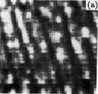
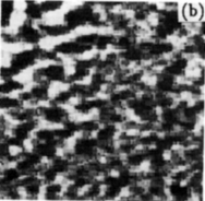
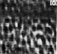
Fig.3 demonstrates OLALS images of FZ Si:P wafer surfaces (11mm2). The pictures and present two sides of the same wafer, one of which was polished in chemico-dynamic way (”finished side”) and the other was polished mechanically up to optical precision grade. The darker the areas in the photographs, the shorter the carrier life is. So the dark stripes in the pictures of the finished side correspond, from our viewpoint, to tracks of underpolished and/or underetched scratches. A very badly damaged layer is registered on the mechanically polished side (the signal from this side was by around 1000 times lower than that from the finished side). The picture gives the micrograph of CZ Si:B wafer surface coated with 1200 Å thick layer of SiO2 (this wafer was taken directly from the technological line of CCD production). The dark spots are likely the images of defective regions.
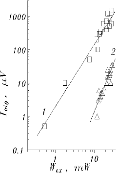
Fig.4 demonstrates the dependence of IR-photodetector signal
on the power of the exciting He-Ne laser for the FZ Si:P wafer
depicted in Fig.3. Two cases are shown: for the finished side
(marked as 1) and for the mechanically polished side (marked as
2). It is seen that in the case (1) the signal is proportional
to the square of the photoexciting laser intensity whereas in
the case (2) the signal is proportional to the third power of
the He-Ne laser intensity. These lines confirm that the SLALS
microscope works with scattered rays and the scattering by the
domain with generated non-equilibrium carriers allows us to make
imaging in the OLALS mode. The cubic dependence (2) has not been
explained yet. Note that the same depence was obtained for the
mechanically polished Ge sample in the work by Kalinushkin et al (1995a).
4. CONCLUSION
It was shown in this paper that the mid-IR-laser microscopy
may become a useful tool for defect investigations in
semiconductors. This method can be easily complemented with such
well developed techniques for defect composition analysis as
measurements of temperature dependencies of LALS (see e.g.
Kalinushkin et al 1995 and Kalinushkin et al 1991).
The measurements of LALS photoexcitation spectra might be also
very useful for this purpose. Such well known technique as
photoluminescence mapping might be used as a complementary
method to the OLALS mode, with the same exciting laser being
used for both techniques and the measurements being made
simultaneously. The tomographic SLALS microscope is also under
development now using the principles of laser heterodyning
(Sawatari 1973 and Protopopov and Ustinov 1985). The methods of
phase contrast and interference microscopies (Françon 1954)
also might appear to be useful.
REFERENCES
Astafiev O V, Buzynin A N, Buvaltsev A I et al 1994a Semicond. 28 (3) 407
Astafiev O V, Kalinushkin V P and Yuryev V A 1994b Proc. SPIE
2332 138
Astafiev O V, Kalinushkin V P and Yuryev V A 1995a Mater. Sci. Eng. (B)
in press
Astafiev O V, Kalinushkin V P and Yuryev V A 1995b Microelectronics
in press
Astafiev O V, Kalinushkin V P and Yuryev V A 1995c Microelectronics
in press
Astafiev O V, Kalinushkin V P and Yuryev V A 1995d J. Tech. Phys. Lett.
in press
Buzynin A N, Butylkina N A, Kalinushkin V P et al 1989 USSR Patent
No.1531766
Buzynin A N, Zabolotskiy S E, Kalinushkin V P et al 1990
Sov. Phys.– Semicond. 24 (2) 264
Françon M 1954 Le Microscope á Contraste de Phase et Microscope Interferentiel (Paris:
Centre National de la Recherche Scientifique)
Kalinushkin V P 1988 Proc. Inst. Gen. Phys. Acad. Sci. USSR Vol.4 Laser
Methods of Defect
Investigations in Semiconductors and Dielectrics (New
York: Nova) pp.1–75
Kalinushkin V P, Murin D I, Astafiev O V et al 1995a Phys.
Chem. Mech. Surf. (4) in press
Kalinushkin V P, Murin D I, Yuryev V A et al 1994 Proc. SPIE
2332 146
Kalinushkin V P, Yuryev V A and Astafiev O V 1995b Mater. Sci. Technol.
in press
Kalinushkin V P, Yuryev V A, Murin D I et al 1991 Semicond. Sci.
Technol. 7 A255
Protopopov V V and Ustinov N D 1985 Laser Heterodyning (Moscow: Nauka)
Sawatari T 1973 Appl.Opt. 12 2768
Voronkov V V, Zabolotskiy S E, Kalinushkin V P et al 1990 J. Cryst.
Growth 103 126
Yuryev V A, Astafiev O V and Kalinushkin V P 1995 Semicond. in press
Yuryev V A and Kalinushkin V P 1995 Mater.Sci.Eng. (B) in press