Rashba spin-splitting control at the surface of the topological insulator Bi2Se3
Abstract
The electronic structure of Bi2Se3 is studied by angle-resolved photoemission and density functional theory. We show that the instability of the surface electronic properties, observed even in ultra-high-vacuum conditions, can be overcome via in-situ potassium deposition. In addition to accurately setting the carrier concentration, new Rashba-like spin-polarized states are induced, with a tunable, reversible, and highly stable spin splitting. Ab-initio slab calculations reveal that these Rashba state are derived from the 5QL quantum-well states. While the K-induced potential gradient enhances the spin splitting, this might be already present for pristine surfaces due to the symmetry breaking of the vacuum-solid interface.
pacs:
71.20.-b, 71.10.Pm, 73.20.At, 73.22.GkTopological insulators, with a gapless topological surface state (TSS) located in a large bulk bandgap, define a new quantum phase of matter Fu et al. (2007); Qi et al. (2008); Moore (2010); Hasan and Kane (2010). Their uniqueness, and their strong application potential in quantum electronic devices, stem from the TSS combination of spin polarization and protection from backscattering Bernevig et al. (2006); Roushan et al. (2009). Bi2Se3 is a three dimensional topological insulator, as theoretically proposed Zhang et al. (2009) and experimentally verified by angle-resolved photoemission spectroscopy (ARPES) and other surface sensitive techniques Xia et al. (2009); Chen et al. (2010); Cheng et al. (2010). Unfortunately, despite great effort in controlling the Se stoichiometry and with it the bulk carrier concentration Butch et al. (2010), unintentional and uncontrolled doping seems to lead to a bulk conductivity that masks the surface electronic properties Hirahara et al. (2010).

ARPES studies also have shown that cleaved sample surfaces and subsurfaces become progressively more electron doped – even in ultra-high vacuum conditions – by either gas adsorption, or formation/migration of defects and vacancies Park et al. (2010); Hsieh et al. (2009). Lastly, the TSS might be completely destroyed when exposed to air, hindering most attempts of material processing and characterization, as well as device fabrication.
Developing new approaches to stabilize and control the surface of these systems is arguably the most critical step towards the exploitation of their topological properties. Some success has been obtained in inducing electron and hole surface doping by a combination of in-situ processing, such as material evaporation and radiation exposure Hsieh et al. (2009); Xu et al. .

The same TSS has also been fabricated on nanoribbons, which have large surface-to-volume ratio Kong et al. (2010). From a different perspective, carefully doped topological insulators can provide a platform to study the interplay between TSS and bulk electron dynamics, which has important implications for TSS control and exploring topological superconductivity Fu et al. (2008).
In this paper, we present a systematic ARPES study of the evolution of the surface electronic structure of Bi2Se3 as a function of time and in-situ potassium evaporation. The deposition of submonolayers of potassium allows us to stabilize the otherwise continually evolving surface carrier concentration. It also leads to a more uniform surface electronic structure, in which well-defined Rashba-like states emerge from the continuum of parabolic-like states that characterizes the as-cleaved, disordered surfaces. This approach provides a precise handle on the surface doping, and also allows tuning the spin splitting of the Rashba-like states. Our density functional theory (DFT) slab calculations reveal that the new spin-split states originate from the bulk-like quantum-well (QW) states of a 5-quintuple-layer (5QL) slab, as a consequence of the K-enhanced inversion symmetry breaking already present for the pristine surface of Bi2Se3.
ARPES measurements were performed at UBC with 21.2 eV linearly polarized photons on an ARPES spectrometer equipped with a SPECS Phoibos 150 hemispherical analyzer and UVS300 monochromatized gas discharge lamp. Energy and angular resolution were set to 10 meV and 0.1∘. Bi2Se3 single crystals, grown from the melt (with carrier density cm-3 Butch et al. (2010)) and by floating zone, were aligned by Laue diffraction and cleaved and measured at pressures better than 510-11 torr and 6 K, unless otherwise specified. No difference was observed for samples grown with different methods. Potassium was evaporated at 6K, with a 6.2 A evaporation current for 30 second intervals Hossain et al. (2008); Fournier et al. (2010). DFT calculations were performed using the linearized augmented-plane-wave method in the WIEN2K package Blaha et al. (2001), with structural parameters from Ref. Zhang et al., 2009. We considered stoichiometric slabs terminated by a Se layer on both sides, representing natural cleavage planes within this material. Spin-orbit interaction is included as a second variational step using scalar-relativistic eigenfunctions as a basis Blaha et al. (2001); exchange and correlation effects are treated within the generalized gradient approximation Perdew et al. (1996).
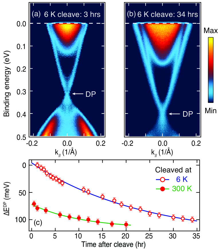
The time evolution of the as-cleaved Bi2Se3 surface is shown in Fig.1. As typically observed by ARPES, and contrary to what is predicted by DFT for fully stoichiometric Bi2Se3 (Fig. 4), even immediately after a 6 K cleave the Fermi level is not in the bulk gap; instead it crosses both TSS and parabolic continuum of bulk-like states. The pronounced time dependence of the data is exemplified by the variation of the Dirac point (DP) binding energy (), which increases from to 400 meV over 34 hours at 510-11 torr and 6 K [Fig. 1(c)]. An exponential fit of versus time indicates that the saturation value meV is reached 46 hours after cleaving. At variance with the time dependence of the TSS, the bottom of the parabolic continuum shifts down by only 30 meV in 34 hours, which provides evidence against the pure surface nature of the continuum. One should note that the pristine position of DP depends also on the cleave temperature: on a sample cleaved at 300 K we found a 70 meV deeper starting position for the DP, although the saturation value is approximately the same as that of the 6 K cleave [Fig. 1(c)].
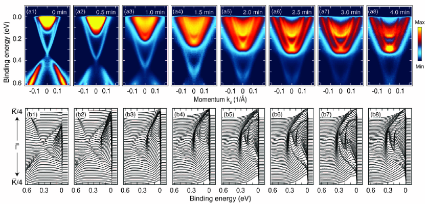
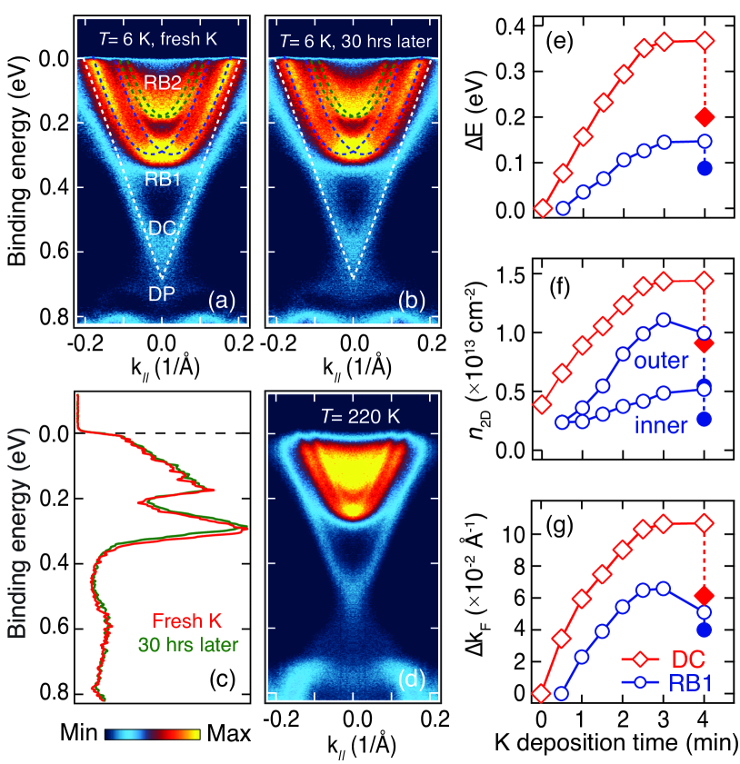
In our ARPES study, the surface time evolution resulted only in the deepening of Dirac cone (DC) and bulk continuum, as a consequence of the sample gaining electrons. Other effects, such as the reported appearance of a 2-dimensional electron gas (2DEG), were not observed Bianchi et al. (2010). More substantial changes are induced by the in-situ evaporation of potassium on the cleaved surfaces, also performed at 6 K to guarantee the highest stability. As a function of K-deposition time, three stages can be identified: Stage I – for moderate K deposition [up to 1 minute, Fig. 2(ab1-ab3)], the DP moves to higher binding energy by electron doping and a sharper parabolic state appears at the edge of the bulk continuum, reminiscent of the proposed 2DEG Bianchi et al. (2010). Stage II: for intermediate K deposition [from 1 to 3 minutes, Fig. 2(ab4-ab7)], as the electron doping further increases, the single parabola splits into a first pair – and then a second one also appears – of sharp parabolic states with an equal and opposite momentum shift away from the point, as in a Rashba type Bychkov and Rashba (1984) splitting [these states are labeled RB1 and RB2 in Fig. 3(a)]. Interestingly, the appearance of the sharp RB1 and RB2 features is accompanied by a suppression of the bulk-like continuum. This emergence of a coherent quasiparticle dispersion from a continuum of incoherent spectral weight indicates that the evaporation of potassium leads to a progressively more uniform surface and subsurface structure. Stage III: for heavy K deposition [beyond 3 minutes, Fig. 2(ab8)], the bottom of RB1 and RB2 as well as are not changing, indicating that the sample cannot be doped any further. The only noticeable effect is a small decrease of spin splitting for RB1 and conversely an increase for RB2, perhaps stemming from a change in hybridization between the two Rashba pairs. As a last remark, during the entire K-deposition process the band velocity of the TSS close to the DP is eV, consistent with previous reports Kuroda et al. (2010).
Before analyzing quantitatively the evolution of the various states upon K deposition, we address the question of the stability of this new surface versus time and temperature cycling. In Fig. 3(a-c) we compare the ARPES data from a 3 minute K-evaporated surface, as measured right after deposition and 30 hours later (during which the sample was kept at 6 K). Other than a smaller than 10 meV shift of the bottom of RB1 [Fig. 3(c)], all spectral features including the TSS have remained exactly the same over the 30 hour interval. This is a remarkable stability, especially when compared to the 365 meV shift induced by the initial K deposition [Fig. 3(e)], and to the more than 100 meV shift observed versus time without any active surface processing [Fig. 1(c)]. This approach might provide a new path to overcome the general instability and self-doping problem of the surface of Bi2Se3, which represents one of the major shortcomings towards the fabrication of topological devices. Temperature effects were studied by slowly warming up the sample, in which case K atoms diffuse and eventually leave the surface, reverting the material back to an earlier stage with lower K coverage. Indeed, as one can see by comparing Fig. 3(d) to Fig. 2(a4), a sample initially K evaporated for 4 minutes at 6 K, and then measured at 220 K after a gradual 36 hour warming up, exhibits ARPES features similar to those obtained directly after a 1.5 minute K deposition at 6 K. This implies that K deposition on Bi2Se3 is also reversible, making it possible to fine tune surface doping, position of the DP, and Rashba spin splitting.
We summarize in Fig. 3(e-g) the K-evaporation evolution of various parameters characterizing the dispersion of DC and Rashba states (empty symbols identify 6 K data, and the filled ones 220 K data). As evident in Fig. 3(e) from the variation of and bottom of RB1, the highest possible doping level is achieved 3 minutes into the K deposition, corresponding to meV and meV.

The K-induced change in surface electron density for the various states can be estimated from the relation between the area of Fermi surface, Brillouin zone, and unit cell, without accounting for spin degeneracy given that all relevant states are spin split. Because at these electron fillings all FS’s are hexagonal, this reduces to , where is the Fermi wavevector along the direction of the BZ (as in Fig. 2).

After 3 minute K evaporation the total sheet carrier density is cm-2 (0.162 electron/BZ), corresponding to the sum of the contributions from DC, and inner-and-outer RB1 and RB2 (1.43, 1.60, and cm-2 respectively). This value is to be compared to cm-2 before K deposition (0.017 electron/BZ), which however only accounts for the DC, given the impossibility of estimating the contribution from the parabolic continuum.
As a last point, from the data presented in Fig. 3(g), and the dispersion of spin-split Rashba bands:
| (1) |
we can estimate the Rashba parameter for RB1. The latter, which depends both on the value of spin-orbit coupling (SOC) and the gradient of the potential Nagano et al. (2009), reflects the size of the spin splitting in momentum space and is here controlled directly by the amount of K deposited on the as-cleaved surfaces. The largest RB1 splitting is observed after 2.5-3 minute K evaporation and is anisotropic: along -, and along -. Fitting the RB1 dispersion along - to Eq. 1, we obtain meV, , and eVÅ. This value is more than twice the Rashba splitting of the Au(111) surface state ( eVÅ), and also larger than the one of the Bi(111) surface state ( eVÅ) Ast et al. (2007).
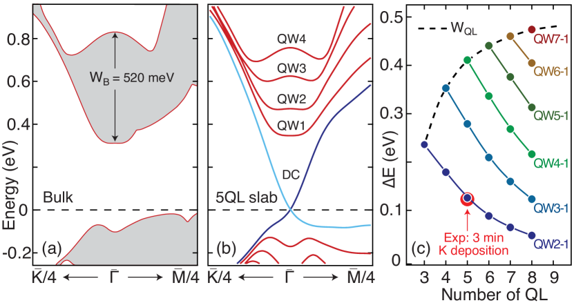
DFT calculations for bulk Bi2Se3, as well as slabs with varying number of QL’s (Fig. 4), provide a detailed explanation for our observations and some interesting insights. Each QL consists of 2 Bi and 3 Se layers alternating along the c axis, with one Se layer in the middle of the QL and the other two on either side. This forms a non-polar structure with a natural cleavage plane between two adjacent Se layers belonging to different QL’s. As shown in Fig. 4(b) for the particular case of a 5QL slab, in addition to the TSS-DC there are 4 QW states, for a total of 5 states matching the number of QL’s. As evidenced by the comparison with the fully projected bulk results in Fig. 4(a), where the TSS is missing due to the absence of the surface, the slab QW states exhibit the same character and energy as the Bi-Se conduction band. However, they are discrete in nature due to quantum confinement, and span a narrower energy range than the corresponding bulk bandwidth meV. The effective slab bandwidth , defined as the energy difference between top and bottom QW states, is asymptotically approaching the bulk value [Fig. 4(c)]; for a proper correspondence with the bulk electronic structure a rather large number of QL’s is needed (i.e., more than 10 QL). Interestingly, the splitting between the DP and the different QW states is extremely sensitive to the number of QL’s. For 5QL we obtain 346 meV QW1-DP and 126 meV QW2-QW1 splittings [Fig. 4(c)], which closely match the 3 minute K-deposition values meV and meV for RB1-DP and RB2-RB1, respectively [as defined from the EDC’s at the point in Fig. 3(a)].
This analysis leads to several important conclusions: (i) The RB1 and RB2 states that emerge from the parabolic continuum are of the same Bi and Se character than those obtained, in the same energy range, in bulk Bi2Se3 calculations. However, because of the observed lack of dispersion Bianchi et al. (2010), and the almost perfect match with QW1 and QW2 energy positions for 5QL [as also emphasized by the comparison between calculation and 3 minute K-deposition datapoint in Fig. 4(c)], these states should be more appropriately thought as the quantum-confined analog of those bulk states, associated with a band-bending over a 5QL subsurface region (47.7 Å). While this region is somewhat disordered – either in its depth and/or carrier concentration – on the as-cleaved surfaces, it becomes progressively better defined upon K evaporation. (ii) Potassium, in addition to doping carriers, also induces a change in , which in turn provides a very direct control knob on both band-bending depth and spin splitting of the Rashba states. (iii) In light of the extent of the subsurface band-bending region, these quantum-confined states should affect more than just surface sensitive experiments. For instance, Rashba spin-split states might have to be accounted for in the interpretation of transport data even from pristine surfaces, although with a much smaller splitting induced solely by the symmetry breaking vacuum-solid interface.
We thank E. Giannini, A.F. Morpurgo, M. Franz, H. Guo, A.N. Yaresko, M.W. Haverkort, and G.A. Sawatzky for discussions, D. Fournier, D. Schneider, H.R. Davis, M. O’Keane, and W.N. Hardy for technical assistance. This study was supported by the Killam Program (A.D.), Sloan Foundation (A.D.), CRC Program (A.D.), Stacie NSERC Fellowship Program (A.D.), NSERC, CFI, CIFAR Quantum Materials, and BCSI. Work at the University of Maryland was supported by NSF-MRSEC (DMR-0520471) and DARPA-MTO award (N66001-09-c-2067).
References
- Fu et al. (2007) L. Fu et al., Phys. Rev. Lett., 98, 106803 (2007).
- Qi et al. (2008) X.-L. Qi et al., Phys. Rev. B, 78, 195424 (2008).
- Moore (2010) J. E. Moore, Nature, 464, 194 (2010).
- Hasan and Kane (2010) M. Hasan and C. Kane, Rev. Mod. Phys., 82, 3045 (2010).
- Bernevig et al. (2006) B. A. Bernevig et al., Science, 314, 1757 (2006).
- Roushan et al. (2009) P. Roushan et al., Nature, 460, 1106 (2009).
- Zhang et al. (2009) H. Zhang et al., Nat. Phys., 5, 438 (2009).
- Xia et al. (2009) Y. Xia et al., Nat. Phys., 5, 398 (2009).
- Chen et al. (2010) Y. L. Chen et al., Science, 329, 659 (2010).
- Cheng et al. (2010) P. Cheng et al., Phys. Rev. Lett., 105, 076801 (2010).
- Butch et al. (2010) N. P. Butch et al., Phys. Rev. B, 81, 241301 (2010).
- Hirahara et al. (2010) T. Hirahara et al., Phys. Rev. B, 82, 155309 (2010).
- Park et al. (2010) S. R. Park et al., Phys. Rev. B, 81, 041405 (2010).
- Hsieh et al. (2009) D. Hsieh et al., Phys. Rev. Lett., 103, 146401 (2009a).
- Hsieh et al. (2009) D. Hsieh et al., Nature, 460, 1101 (2009b).
- (16) S.-Y. Xu et al., arXiv:1101.3985 .
- Kong et al. (2010) D. Kong et al., Nano Lett., 10, 329 (2010).
- Fu et al. (2008) L. Fu et al., Phys. Rev. Lett., 100, 096407 (2008).
- Hossain et al. (2008) M. A. Hossain et al., Nat. Phys., 4, 527 (2008).
- Fournier et al. (2010) D. Fournier et al., Nat. Phys., 6, 905 (2010).
- Blaha et al. (2001) P. Blaha et al., in An augmented plane wave plus local orbitals program for calculating crystal roperties, edited by K. Schwarz (Technical University of Wien, Vienna, 2001).
- Perdew et al. (1996) J. P. Perdew et al., Phys. Rev. Lett., 77, 3865 (1996).
- Bianchi et al. (2010) M. Bianchi et al., Nat. Commun., 1, 128 (2010).
- Bychkov and Rashba (1984) Y. A. Bychkov and E. I. Rashba, J. Phys. C, 17, 6039 (1984).
- Kuroda et al. (2010) K. Kuroda et al., Phys. Rev. Lett., 105, 076802 (2010).
- Nagano et al. (2009) M. Nagano et al., J. Phys.: Condens. Matter, 21, 064239 (2009).
- Ast et al. (2007) C. R. Ast et al., Phys. Rev. Lett., 98, 186807 (2007).