Corresponding author: S. Burger
URL: http://www.zib.de/en/numerik/computational-nano-optics.html
URL: http://www.jcmwave.com
Email: burger@zib.de
Rigorous Simulations of 3D Patterns on
Extreme Ultraviolet Lithography Masks
Abstract
Simulations of light scattering off an extreme ultraviolet lithography mask with a 2D-periodic absorber pattern are presented. In a detailed convergence study it is shown that accurate results can be attained for relatively large 3D computational domains and in the presence of sidewall-angles and corner-roundings.
keywords:
3D rigorous electromagnetic field simulations, optical metrology, computational lithography, EUV scatterometry, finite-element methodsThis paper will be published in Proc. SPIE Vol. 8083 (2011) 80831B (Modeling Aspects in Optical Metrology III; B. Bodermann, H. Bosse, R. M. Silver, Editors, DOI: 10.1117/12.889831), and is made available as an electronic preprint with permission of SPIE. One print or electronic copy may be made for personal use only. Systematic or multiple reproduction, distribution to multiple locations via electronic or other means, duplication of any material in this paper for a fee or for commercial purposes, or modification of the content of the paper are prohibited.
1 Introduction
Extreme ultraviolet (EUV) lithography at a wavelength of about 13 nm is expected to replace DUV photolithography for manufacturing features on integrated circuits with critical dimensions as small as 22 nm or beyond. Rigorous simulations of light propagation through photomasks are an essential component in optical metrology of such structures. Rigorous simulations are also used for optimizing feature geometries on masks for improving lithographic process stability and for resolution enhancement in printing of sub-wavelength features (computational lithography).
In deep ultraviolet (DUV, wavelength of about 193 nm) lithography and metrology simulations a main challenge consists in accurate resolution of light fields in the presence of complex 3D absorbing structures of high refractive index-contrasts. In the EUV regime available materials exhibit far lower refractive index-contrasts. On the one hand this simplifies computations because high field enhancements and field singularities do not occur. On the other hand the limits to available optical materials in the EUV regime leads to additional challenges for rigorous simulations: (i) Computational domain sizes increase due to the fact that absorber structures need larger volumes (relative to the cubic illumination wavelength). (ii) Deviations from ideal geometries like sidewall-angles have a larger effect on the diffraction spectra. (iii) EUV masks are typically mounted on multi-layer mirrors with a high number of single layers. This again increases 3D computational domain size and complexity.
We have developed a general finite-element (FEM) Maxwell solver which also allows to address 3D EUV simulation tasks. The solver incorporates higher-order edge-elements, domain-decomposition methods and fast solution algorithms for solving time-harmonic Maxwell’s equations in various problem formulations (e.g., resonance, scattering type problems) [1]. Previously the solver has been used for the study and metrological investigations of EUV line masks (1D-periodic patterns) [2, 3, 4, 5]. In this contribution we report on rigorous electromagnetic field simulations of 2D-periodic arrays of absorber structures on EUV masks. In a convergence study we show that highly accurate results can be attained.
This paper is structured as follows: The investigated mask setup is described in Section 2. In Section 3 a convergence study is performed: In Section 3.1 highly accurate results (reference solution) for the scattering response of a line mask are generated using a 2D light scattering solver. Consistent solutions are generated using two different approaches: (i) scattering off the full structure, and (ii) scattering off the absorber structure and the multi-layer mirror coupled through a rigorous domain-decomposition approach [6]. In Section 3.2 the previously obtained accurate results are used as reference solution to investigate convergence of the full 3D light scattering solvers. In Section 4 the solver is used for simulation of the full 3D problem of a 2D-periodic array of absorber structures on an EUV mask. Again, numerical convergence of the obtained results is investigated. Numerical simulation results are tabulated in the Appendix.
2 Investigated setup
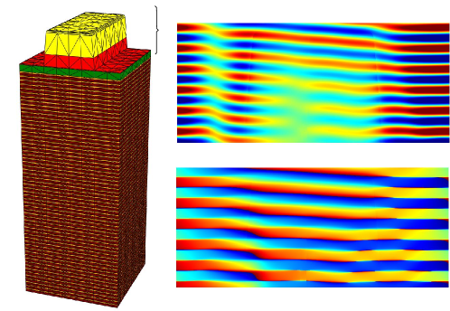
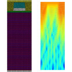
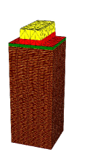
The investigated structures consist of an absorber stack on a multi-layer mirror (consisting of a total of 120 layers). Figure 1 shows a 3D mesh of the geometry and a typical electric field distribution in a part of the stack. A schematics of the setup is shown in Figure 2. This study is concerned with numerical properties of the FEM simulation method, therefore only one fixed setting of the material and stack parameters is investigated, and only two fixed settings of lateral placement of absorber structures on the multi-layer (a 1D-periodic line mask and a 2D-periodic pattern). The chosen geometrical and material parameters of the physical setting are given in Table 1. For modeling unpolarized illumination, the near-fields corresponding to illumination with S- and P-polarized plane waves at 13.4 nm vacuum wavelength and at an (in-plane) angle of incidence of 4 degree are computed, and an incoherent superposition of the fields is performed. Highly accurate, rigorous numerical simulation of this 3D setup is challenging because the total size of the 3D computational domain is about which corresponds to about cubic wavelengths.
| material | height | n | k | |
|---|---|---|---|---|
| air | 1 | 0 | ||
| absorber | nm | 0.93368 | 0.03791 | deg, nm |
| buffer | nm | 0.97468 | 0.01261 | deg |
| oxide | nm | 0.97468 | 0.01261 | |
| capping | nm | 1.00024 | 0.00182 | |
| multi-layer (Mo) | nm | 0.92373 | 0.0061 | 60 layers |
| multi-layer (Si) | nm | 1.00024 | 0.00182 | 60 layers |
| substrate | 0.97908 | 0 | ||
| lateral dimensions | 88 nm | |||
| 110 nm | ||||
| 176 nm | ||||
| 176 nm | ||||
| illumination | angle of incidence | deg | ||
| wavelength | nm | |||
3 Convergence study
3.1 Reference solution: 1D line mask
The aim of this paper is to demonstrate which accuracy of rigorous electromagnetic field simulations can be reached for relatively large computational domains. For the general 3D scattering problem (2D-periodic absorber pattern) as described in Section 2 no analytical solution exists. No alternative results are available which can be used as quasi-exact results in order to quantify numerical errors of a 3D simulation result. Therefore the problem is analyzed as follows: First, results for a linemask setup are generated using a rigorous FEM solver on a 2D computational domain. The FEM solver has been compared to other simulation methods, and it also converges with the expected convergence order, therefore it can be assumed that the obtained result is quasi-exact. Then, results for the same physical setting (line mask) are generated on a 3D computational domain. The quasi-exact result from the 2D setup is used to measure the reached numerical accuracy of the 3D results. It is expected that the accuracy of results of a 2D-periodic pattern with a computational domain of comparable size will be similar to the accuracy obtained for the linemask.
3.1.1 1D line mask: 2D computational domain
The electromagnetic near-field of the setup as defined in Section 2 is simulated using a 2D computational domain (the structure is invariant in the third dimension). Figure 3 (left) shows a typical initial spatial mesh and a graphical representation of a computed near-field intensity distribution. Various post-processes are used to deduce quantities of interest from the electric near-field :
-
•
The amplitudes of all propagating, reflected diffraction orders are evaluated by Fourier integration over the complex electric field at the upper boundary of the computational domain. The propagating Fourier mode is characterized by the complex amplitude , the wavevector and the diffraction order .
Here, the boundary of the computational domain spans from to . The Fourier modes are normalized to the width (resp. area) of the respective computational domain boundary, . The reflected power is then given by , with the angle between the surface normal and the wavevector of the respective diffraction order, , impedance , permittivity and permeability ..
-
•
The amplitudes of all transmitted diffraction orders are obtained in the same way, and the transmitted power is obtained.
-
•
The electric field energies in all sub-domains of the computational domain, , are computed by field integration over the complex electric field distribution :
The absorbed power is then given by , with the angular frequency and vacuum speed of light .
The incident power is given by , with the amplitude of the incident S- and P-polarized plane waves. Power conservation is expected, i.e., with increasing numerical resolution the sum of incoming, outgoing and absorbed power flux should converge to zero, , .
In scatterometric applications and in computational lithography applications, the quantities of interest are typically the amplitudes of the diffraction orders (because these are detected in a scatterometric setup, resp. because these enter the optical imaging system). Therefore this study concentrates on convergence of the results with respect to both, power conservation and intensities of some few diffraction orders.
Table Appendix: Tabulated simulation results shows numerical results: Intensities of some exemplary diffraction orders, of reflected power flux and of power conservation have been computed from near-fields obtained at different numerical resolutions. For computing these fourth-order finite-elements are chosen (polynomial degree of the finite-element ansatzfunctions, defined on the patches of the discretized geometry, ) and solutions on meshes with different refinement are computed (where adaptive mesh refinement steered by an automatic, residual-based error-estimator has been choosen as refinement strategy). With increasing mesh refinement the number of geometrical patches is increased which leads to a better resolution of the computed electromagnetic near-field and the derived quantities, and which leads to increased number of unknowns of the sparse system of equations resulting from the FEM discretization. Very high numerical accuracy is reached for few refinement steps, with total numbers of unknowns below one million and with typical computation times on standard computer hardware in the range of few minutes. The saturation in power conservation error at a very low error level, , may be due to floating point precision errors which may come into play at this very high accuracy level. Parts of this data is also displayed graphically in Figure 3. The displayed relative error of the intensity of diffraction order is defined as , where the FEM simulation result at highest numerical resolution is chosen as quasi-exact result, .
3.1.2 1D line mask: 2D Domain decomposition results
A significant part of the computational effort necessary for the computation of the near-field solution as displayed in Figure 3 is necessary for computation of the field distribution in the multi-layer stack. This region is essentially only a 1D-structured geometry. Therefore wave propagation in this region can be treated quasi-analytically or by solving only 1D FEM problems. However, the absorber pattern has a higher dimensionality. It has been shown that a rigorous domain-decomposition algorithm can use these properties of the problem for reducing significantly the computational effort (in terms of numbers of unknowns and computation times) [6].. The domain-decomposition algorithm essentially operates by dividing the computational domain as shown schematically in Figure 2 into the multi-layer mirror and the absorber structure. These two domains are then coupled via the electromagnetic field coupled back and forth between the domains, and convergence is reached by iterative improvement of the field approximations.
The domain-decomposition algorithm is applied to the 2D setup, as discussed above. Table Appendix: Tabulated simulation results shows some of the results (in this case power conservation is not checked, as the absorbed power in the multi-stack mirror is not automatically evaluated by the software in the domain-decomposition setup). Figure 4 displays convergence of the diffraction intensities and of the reflected power. As quasi-exact value the near-field result with highest numerical resolution has been chosen.
As can be seen from Table Appendix: Tabulated simulation results, the quantitative results agree between the domain-decomposition setup and the full 2D setup up to a relative accuracy of about in all investigated quantities. With the domain-decomposition setup, very accurate results can be obtained at relatively low computational effort.
3.2 3D simulations: 1D line mask
The main purpose of the previous sections was to compute an accurate reference solution for rigorous EMF simulations on a 3D computational domain. In this section the light scattering response of the same EUV line-mask is computed using a 3D computational domain. The problem is again approached using, first, a full computational domain and, second, a separation in multi-layer mirror and absorber using a domain-decomposition solver. A 3D problem which cannot be reduced to a 2D setting will be treated in Section 4.
3.2.1 1D line mask: Full 3D computational domain
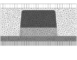
First, the EUV line-mask is revisited using a 3D computational domain containing both, the absorber structure and the multi-layer mirror. Figure 5 shows a mesh discretizing the geometry (generated automatically with the mesh generator JCMgeo). For the 3D setup the mesh consists of prismatoidal elements (instead of triangular elements as in the 2D setups). Simulations of the same physical setup have been performed using different spatial meshes with increasing mesh refinement and using finite-element ansatz-functions with varying polynomial degree (both, increasing and increasing mesh resolution in general leads to higher accuracy). The numerical results on intensities of several diffraction orders, on reflected power and on power conservation are given in Table Appendix: Tabulated simulation results. From the results it can be seen that the first three significant digits of accuracy are reached for all investigated quantities. Considering the large computational domain with a size of the order of 10,000 cubic wavelengths this is a notable result which can be explained by the good convergence properties of higher-order finite-elements.
Figure 5 shows how the relative errors of the diffraction intensities converge with number of unknowns of the problem and how the power conservation error converges towards zero. As quasi-exact reference for the diffraction intensities, results from Sec. 3.1.2 are used.
3.2.2 1D line mask: 3D Domain decomposition results
In this Section simulation of the line-mask using a 3D computational domain and the domain-decomposition algorithm as described in Section 3.1.2 is demonstrated. Figure 6 shows a typical mesh discretizing the geometry. The numerical results are given in Table Appendix: Tabulated simulation results. Figure 6 (center) shows the convergence of the (absolute) error of the diffraction intensities, (for amplitudes of the incident light fields). Accuracies in the range of are reached. For the relative accuracy of the total reflected power, an accuracy below is reached at highest numerical resolution. As quasi-exact reference for the diffraction intensities, results from Sec. 3.1.2 are used. As can be seen from the table high numerical accuracy (with agreement of three to four significant digits even in low-power diffraction orders) is reached.
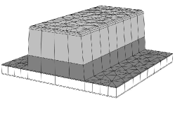
4 Simulations of 2D-periodic patterns on an EUV mask
In the previous Section it has been shown that the 3D light scattering solver module of JCMsuite generates numerical results which converge well to quasi-exact results obtained with the 2D light scattering module (which has been compared and benchmarked to independent rigorous methods and implementations [7, 8, 9]). In this Section a 3D setup is investigated which cannot be reduced to a 2D computational domain: Figure 7 shows the investigated setup. All parameters of the setup are detailed in Table 1. The setup and execution of the simulations is performed as in Section 3.2.2. Table Appendix: Tabulated simulation results presents simulation results for simulation on grids of different refinement levels and for finite-element ansatzfunctions of polynomial degree . For this setup, also out-of-plane scattering takes place due to the 3D nature of the absorber block, therefore also some exemplary out-of-plane diffraction orders are included in the tabulation (e.g., diffraction order , first order diffraction in - and in -direction). As can be seen from the tabulated results and from the convergence of the numerical errors of the computed diffraction orders as displayed in Fig. 7, a high numerical accuracy is reached. Here, as quasi-exact result for the convergence plots, the FEM simulation result at highest numerical resolution has been chosen. The first three to four digits of the intensities even of relatively weak diffraction orders (at five orders of magnitude lower intensity than the most intense, zero diffraction order) are accurately computed.
5 Conclusion
Rigorous simulations of light scattering off 2D-periodic patterns on EUV masks have been performed. In a detailed convergence study it has been shown that high accuracies can be reached for the simulated intensities of the diffraction spectrum. This opens a prospect for scatterometric measurements of 3D patterns on EUV masks using FEM simulations for pattern reconstruction. Future work will concern application of reduced basis methods [10] for significantly reducing computation times for this simulation task. This will open prospects for online reconstruction of 3D patterns on EUV masks.
Acknowledgments
The authors would like to acknowledge the support of European Regional Development Fund (EFRE) / Investitionsbank Berlin (IBB) through contracts ProFIT 10144554 and 10144555.
References
- [1] Burger, S., Zschiedrich, L., Pomplun, J., and Schmidt, F., “JCMsuite: An adaptive FEM solver for precise simulations in nano-optics,” in [Integrated Photonics and Nanophotonics Research and Applications ], ITuE4, Optical Society of America (2008).
- [2] Pomplun, J., Burger, S., Schmidt, F., Zschiedrich, L. W., Scholze, F., and Dersch, U., “Rigorous FEM-simulation of EUV-masks: Influence of shape and material parameters,” in [Photomask Technology ], 6349-128, Proc. SPIE (2006).
- [3] Scholze, F., Laubis, C., Dersch, U., Pomplun, J., Burger, S., and Schmidt, F., “The influence of line edge roughness and CD uniformity on EUV scatterometry for CD characterization of EUV masks,” Proc. SPIE 6617, 66171A (2007).
- [4] Tezuka, Y., Cullins, J., Tanaka, Y., Hashimoto, T., Nishiyama, I., and Shoki, T., “EUV exposure experiment using programmed multilayer defects for refining printability simulation,” 6517, Proc. SPIE (2007).
- [5] Scholze, F., Laubis, C., Ulm, G., Dersch, U., Pomplun, J., Burger, S., and Schmidt, F., “Evaluation of EUV scatterometry for CD characterization of EUV masks using rigorous FEM-simulation,” 6921, 69213R, Proc. SPIE (2008).
- [6] Schädle, A., Zschiedrich, L., Burger, S., Klose, R., and Schmidt, F., “Domain decomposition method for maxwell’s equations: Scattering off periodic structures,” J. Comp. Phys. 226, 447 (2007).
- [7] Burger, S., Köhle, R., Zschiedrich, L., Gao, W., Schmidt, F., März, R., and Nölscher, C., “Benchmark of FEM, waveguide and FDTD algorithms for rigorous mask simulation,” in [Photomask Technology ], Weed, J. T. and Martin, P. M., eds., 5992, 378–389, Proc. SPIE (2005).
- [8] Hoffmann, J., Hafner, C., Leidenberger, P., Hesselbarth, J., and Burger, S., “Comparison of electromagnetic field solvers for the 3d analysis of plasmonic nano antennas,” in [Modeling Aspects in Optical Metrology ], Bosse, H. and Bodermann, B., eds., 7390, 73900J, Proc. SPIE (2009).
- [9] Lockau, D., Zschiedrich, L., and Burger, S., “Accurate simulation of light transmission through subwavelength apertures in metal films,” J. Opt. A: Pure Appl. Opt. 11, 114013 (2009).
- [10] Pomplun, J. and Schmidt, F., “Accelerated a posteriori error estimation for the reduced basis method with application to 3d electromagnetic scattering problems,” SIAM Journal on Scientific Computing 32(2), 498–520 (2010).
Appendix: Tabulated simulation results
| N | [sec] | ||||||
|---|---|---|---|---|---|---|---|
| 246686 | 25 | 3.024847507e-01 | 1.906706398e-01 | 2.7206962e-02 | 1.0884158e-03 | 0.38217497 | 4.01e-05 |
| 514148 | 192 | 3.024385681e-01 | 1.906496392e-01 | 2.7206380e-02 | 1.0888107e-03 | 0.38212772 | 1.01e-06 |
| 1110332 | 453 | 3.024389867e-01 | 1.906489203e-01 | 2.7206608e-02 | 1.0884332e-03 | 0.38212733 | 2.69e-09 |
| 2166904 | 955 | 3.024389384e-01 | 1.906489036e-01 | 2.7206569e-02 | 1.0884331e-03 | 0.38212721 | 7.16e-09 |
| 4115942 | 1489 | 3.024389304e-01 | 1.906489032e-01 | 2.7206565e-02 | 1.0884326e-03 | 0.38212720 | 5.24e-09 |