Strain driven onset of non-trivial topological insulating states in Zintl Sr compounds (=Pb, Sn)
Abstract
We explore the topological behavior of the binary Zintl phase of the alkaline earth metals based compounds Sr2Pb and Sr2Sn using both standard and hybrid density functional theory. It is found that Sr2Pb lies on the verge of a topological instability which can be suitably tuned through the application of a small uniaxial expansion strain ( 3%). The resulting non-trivial topologically insulating state display well-defined metallic states in the Sr2Pb(010) surface, whose evolution is studied as a function of the film thickness.
pacs:
71.20.-b, 73.43.-f, 73.20.-rTopological insulators1 ; 2 ; 3 ; 4 ; 5 ; 7 (TI) are a new quantum state of matter characterized by the existence of gapless surface states sheltered against destructive scattering effects by time-reversal symmetry. Since the discovery of two dimensional TI behaviors of HgTe-based quantum wells 26 ; 27 , several families of topological materials have been theoretically predicted and experimentally realized afterwards.1 ; 30 The variety of insulating materials displaying topological features includes alloys28 ; 5 , Bi2Te3, Bi2Se3 and Sb2Te3 binary compounds 7 ; 72 ; 29 ; 30 ; 73 , ternary heavy-metals based compounds such as TlBiTe2, TlBiSe2 31 ; 32 ; 33 , and PbBi2Se4 34 ; 35 , and ternary rare-earth chalcogenides (LaBiTe3) 36 , and another honeycomb-lattice type of ternary compounds (LiAuSe) Zhanghj . All these materials are characterized by a layered structure stacked along the -axis of the centrosymmetric hexagonal lattice, similar to the structure of Bi2Se3. In addition, other ternary TIs have been recently predicted such as the non-centrosymmetic cubic zinc-blende HgTe-like phase (half-Heusler compounds 37 ; 38 ; 39 and I-III-VI2 and II-IV-V2 chalcopyrite semiconductors such as AuTlTe2 40 ; 41 ), and Ca3NBi with a centrosymmetric antiperovskite structure Sun . Although a large number of ternary TI have been found31 ; 32 ; 33 ; 34 ; 35 ; 36 ; 37 ; 38 ; 39 ; 40 ; 41 , up to now, binary TIs are only limited to three classes: Bi1-xSbx alloys and the family of Bi2Te3, Bi2Se3 and Sb2Te3 as well as Ag2Te 42 . In searching for new TI materials we have focused our attention on binary heavy-element-based small band gap semiconductors. One of the simplest way to realize a binary heavy-element-based closed-shell semiconductor is with an alkaline earth element (M = Mg, Ca, Sr, and Ba) which donates its s valence electron to a IV group element (X = Si, Ge, Sn and Pb). These are the so-called Zintl compounds.
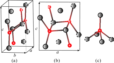
The Zintl compounds crystallize in a simple orthorhombic crystal structure Bruzzone ; Eckerlin , as illustrated in Fig. 1. The atoms surround the atoms in a slightly distorted trigonal-prismatic coordination. The coordination sphere is augmented by the three atoms situated on the rectangular faces of these prisms (tri-capped trigonal prism). Along the direction the prisms are condensed via common edges while they share common triangular faces along the direction. The semiconducting character of these compounds originates from their closed-shell nature, with 6 valence electrons (2s2+p2) per formula unit [].
We have performed band structure calculations using the Perdew-Burke-Ernzerhofpbe (PBE) based standard and hybrid (HSEhse ) density functional theory (DFT) as implemented in the Vienna Ab initio Simulation Package (VASP) vasp1 ; vasp2 , with the inclusion of relativistic spin-orbit coupling (SOC) effects. Within the HSE method, the many body exchange and correlation functional is constructed by mixing 25% exact Hartree-Fock exchange with 75% PBE, and the long-range Coulomb interaction is suitably screened according to the parameter (here = 0.3 Å -1). By using the experimental lattice constants we have relaxed all atomic positions using a very dense k-points mesh (up to 4200 kpoints).
Our preliminary PBE-based research of possible topological features in this class of materials revealed that two members of the Zintl family (Sr2Pb and Ba2Pb) exhibit promising fingerprints of TI behaviors whereas the remaining compounds are either trivial insulator (Ca2Ge, Sr2Ge,Ca2Sn and Sr2Sn) or semimetal (Ba2Ge, Ca2Pb and Ba2Sn). Therefore in the following we focus our analysis on these two specific Zintl compounds: Sr2Pb and Sr2Sn.
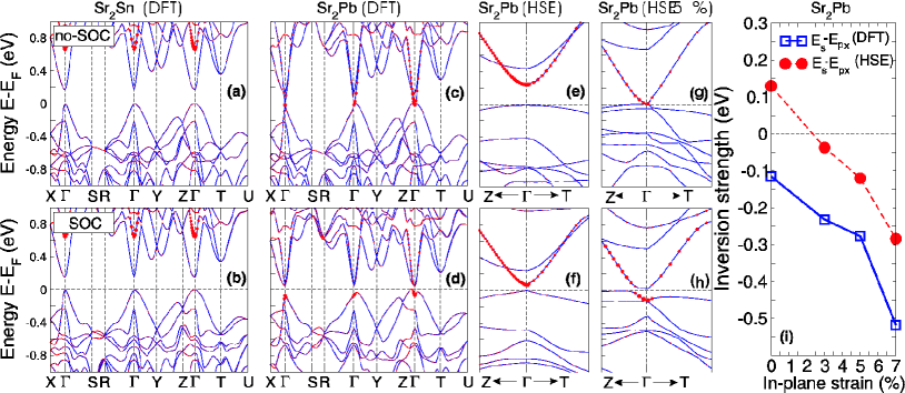
The DFT band structures with and without SOC effects are compared in Fig. 2(a-d). The inclusion of SOC effects does not affect the overall electronic character of Sr2Sn [Fig. 2 (a,b)] which remains semiconductor with a small bandgap at ( 0.15 eV) opened between occupied Sn states and highly dispersive Sr -like empty orbitals (mostly ). By replacing Sn with the isoelectronic heavier element Pb the band structure changes dramatically, as schematically depicted in Fig.3 (a). Without SOC, Sr2Pb displays a metallic (gapless) state [Fig. 2(c)] whereas the inclusion of SOC [Fig. 2(d)] opens a band gap of about 100 meV at (the indirect gap is about 50 meV), as a consequence of the anti-crossing between the conduction band minimum (CBM) and valence band maximum (VBM), a typical fingerprint of the SOC-induced formation of topological insulating states. The major differences between the electronic structure of Sr2Sn and Sr2Pb resides in the orbital character of the valence and conduction bands near as highlighted by the (red) solid circles in the band plot of Fig.2(a-d): in Sr2Sn the states with a predominant -like character lie about 0.5 eV above the Fermi Level [see Fig. 2(a,b)], whereas in Sr2Pb these states are pushed down in energy and eventually hybridize the VBM at thus inducing the anti-crossing feature responsible for the opening of the gap and the creation of a TI state. The downward shift of the -states is accompanied by a upward shift of the heavy metal bands which ultimately intermix with the Sr states as schematized in Fig. 3 (a).
As recently reported by Zunger and coworkersVidal , the identification of band-inverted TI26 ; 27 on the basis of conventional DFT may lead to false-positive assignment if the band inversion strength is not large enough, due to the well documented bandgap underestimation problem. For this reason we have revisited the electronic dispersion of Sr2Pb by HSE, which indeed yields a substantially different physical picture, as illustrated in Fig. 2(e,f). HSE finds a much larger bandgap (0.25 eV) which is reduced to 0.13 eV with the inclusion of SOC effects, and, most importantly, prevent the occurrence of band inversion between the x-like and -like states as schematically illustrated in Fig. 3(b). The states remain well localized on the bottom of the conduction band [Fig. 2(e,f)]: Sr2Pb is not a TI in its native phase. DFT wrongly stabilizes a spurious TI solution because of the relatively small band inversion strength [0.12 eV, see Fig.2(a)]. Though HSE is expected to provide a generally more accurate description of band dispersion in small bandgap insulators, future optical experiment will be necessary in order to validate our first principles findings.
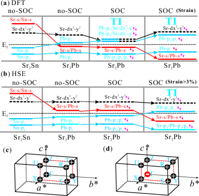
To explore possible routes for designing a TI phase in the native phase of Sr2Pb, we carried out a series of calculations applying strain, a gap-engineering technique which was successful when applied to zero-gap semiconductors such as ternary Heusler compounds38 and Ca3NBi. Sun We have chosen to study the effect of uniaxial strain () in the -plane, by leaving the -axis unconstrained (free to relax) in order to simulate at best the experimental condition for thin film growth. The results, obtained by HSE and shown in Fig. 2(g and h), indicate that for relatively small uniaxial strain larger than 3% Sr2Pb can be tuned towards a TI phase. The role of SOC effects is essential to open a small gap around and to induce an inverted band order. The -like states shift downward below the Fermi level and becomes occupied and, simultaneously, the px-like states become unoccupied and promoted at higher energy. This kind of inverted band behavior can be ascribed to the fact that the strain-induced expansion in the ac-plane reduces the crystal field effect, resulting in the less hybridization between s- and p-like states and stabilizing the s-like state at lower energy, as evidenced in Fig. 2(e) and (g). In such a way, the spin-orbit coupling strength is now enough to invert the band order between s-like and p-like states at (c.f., Fig. 2(f) and (h)). For larger strains up to 7% the TI state is preserved and further stabilized as inferred by the evolution of the band inversion strength as a function of strain reported in Fig. 2(i) at both, DFT and HSE levels.
Beside the band inversion, an alternative way to identify TI states is the parity criteria proposed by Fu and Kane 28 . Considering that orthorhombic Pnma posses the inversion symmetry this criteria can be applied and will serve as a further support for our analysis. The product of the parities of the Bloch wave function for the occupied bands at all eight time reversal invariant momenta (TRIM), illustrated in Fig. 3(c,d), suggest that at six TRIMs (X, Y, Z, S, T and U) all bands share the same doubly degenerate character, whereas the TRIM R is found to be fourfold degenerate. Therefore all these seven TRIMs display a positive (”+”) global parity. At the situation is different: the product of the parities is ”+” and ”-” depending on whether or not the band inversion occurs, in consistency with the HSE band structure interpretation [Fig. 3(c,d)]. We can therefore trustfully conclude that distorted orthorhombic Sr2Pb is a topological non-trivial insulator with 2 index (1; 000). Strained-driven gap-engineering on Sr2Sn dose not results in any topological transition: Sr2Sn remains a conventional semiconductor.
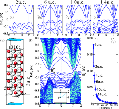
After discussing the onset of topological features in the bulk phase of distorted Sr2Pb we turn our attention to the surface properties focusing on the non-polar (010) termination. Considering that both DFT and HSE lead to an essentially identical TI state in strained Sr2Pb and that SOC-HSE calculations for thick slabs are computationally very demanding (if not prohibitive at all) we study the surface band structure at DFT level only. The results on the Sr2Pb(010) surface are summarized in Fig. 4, which shows that very thick slabs have topologically protected surface metallic states which remain robust with increasing the film thickness, thus corroborating the conclusion of the bulk parity analysis and the inverted band order. The evolution of the band structure as a function of the film thickness show a very peculiar behavior. Already at low film thickness surface related states emerge in a small energy window ( 200 meV) around the Fermi level. This leads to a quenching of the bandgap as compared to the bulk value (130 meV). The bandgap is then progressively reduced by increasing the slab thickness. Though for a thickness of 22 unit cell (u.c.) [Fig. 4(f)] the gap is almost completely suppressed (10 meV), it is necessary to increase the thickness up to 100 u.c. in order to fabricate a well-defined metallic film [Fig. 4(g)]. At the critical thickness of 100 u.c. the lowest conduction band and the highest valence band meet at the Fermi level at and establishes a single-Dirac-cone-like metallic surface state.
In conclusion, our computational study has disclosed the non-trivial topological nature of the binary compound Sr2Pb. The detailed analysis of the bulk and surface structural and electronic properties is of relevance for the design principles of TI and provides helpful insight for tunability of TI states in trivial insulator by gap-engineering techniques. We believe that our findings will encourage immediate experimental investigations.
Acknowledgement. The authors are grateful for supports from the “Hundred Talents Project” of Chinese Academy of Sciences and from the project of the NSFC of China (Grand Numbers: 51074151 and 51050110444) as well as Supercomputing Center of Chinese Academy of Sciences (including Shenyang branch) and a local HPC cluster in the Materials Process Simulation Division, IMR of CAS as well as the Vienna Scientific Cluster (VSC) in Austria. F.Z. acknowledges the supports from the 973 program of China (No. 2007CB925000).
References
- (1) M. Z. Hasan, C. L. Kane, Rev. Mod. Phys. 82, 3045 (2010).
- (2) J. E. Moore, Nature 464, 194 (2010).
- (3) Zhang, S. -C. Physics 1, 6 (2008)
- (4) D. Hsieh, D. Hsieh, Y. Xia, L. Wray, D. Qian, A. Pal, J. H. Dil, F. Meier, J. Osterwalder, C. L. Kane, G. Bihlmayer, Y. S. Hor, R. J. Cava and M. Z. Hasan. Science, 323, 5916, (2009).
- (5) D. Hsieh, D. Qian, L. Wray, Y. Xia, Y. S. Hor, R. J. Cava, and M. Z. Hasan, Nature 452, 970 (2008).
- (6) Y. Xia, D. Qian, D. Hsieh, L.Wray, A. Pal, H. Lin, A. Bansil, D. Grauer, Y. S. Hor, R. J. Cava and M. Z. Hasan, Nature Physics 5, 398 (2009).
- (7) D. Hsieh, J.W. McIver, D. H. Torchinsky, D. R. Gardner, Y. S. Lee, and N. Gedik, Phys. Rev. Lett, 106, 057401 (2011).
- (8) Y. Xia, D. Qian, L. Wray, D. Hsieh, G. F. Chen, J. L. Luo, N. L. Wang, and M. Z. Hasan, Phys. Rev. Lett, 103, 037002 (2009).
- (9) B. A. Bernevig, T. L.Tughes and S.-C. Zhang, Science, 314, 1757 (2006).
- (10) M. König, S. Wiedmann, C. Brüne, A. Roth, H. Buhmann, L. Molenkamp, X. -L. Qi, and S. -C. Zhang, Science, 318, 766 (2007).
- (11) Y. L. Chen, J. G. Analytis, J. -H. Chu, Z. K. Liu, S.-K. Mo, X. -L. Qi, H. J. Zhang, D. H. Lu, X. Dai, Z. Fang, and S. -C. Zhang, Science, 325, 178, (2009).
- (12) L. Fu and C.L. Kane, Phys. Rev. B, 76, 045302 (2007).
- (13) H. J. Zhang, C.-X. Liu, X.-L. Qi, X. Dai, Z. Fang, and S. -C. Zhang, Nature Physics, 5, 438 (2009).
- (14) B. Yan, C.-X. Liu, H.-J. Zhang, C.-Y. Yam, X.-L. Qi, T. Frauenheim, and S.-C. Zhang, Europhys. Lett. 90, 37002 (2010).
- (15) Y. Chen, Z. Liu, J. Analytis, J. Chu, H. Zhang, S. Mo, R. Moore, D. Lu, I. Fisher, S. Zhang, arXiv:1006.3843v1 (2010).
- (16) T. Sato, K. Segawa, H. Guo, K. Sugawara, S. Souma, T. Takahashi, Y. Ando, Phys. Rev. Lett. 105, 136802 (2010).
- (17) S.-Y. Xu, L.A. Wray, Y. Xia, R. Shankar, A. Petersen, A. Fedorov, H. Lin, A. Bansil, Y. S. Hor, R. J. Cava, and M. Z. Hasan, arXiv: 1007.5111 (2010).
- (18) H. Jin, J.-H. Song, A. J. Freeman and M. G. Kanatzidis, Phys. Rev. B, 83, 041202(R) (2011).
- (19) B. H. Yan, H. -J. Zhang, C. -X. Liu, X. -L. Qi, T. Frauenheim, and S.-C. Zhang, Phys. Rev. B,82, 161108(R) (2010)
- (20) H.-J. Zhang, S. Chadov, L. Muchler, B. Yan, X.-L. Qi, J. Kübler, S.-C. Zhang, and C. Felser, Phys. Rev. Lett., 106, 156402 (2011).
- (21) H. Lin, L. A. Wray, Y. Xia, S. Xu, S. Jia, R. J. Cava, A. Bansil, and M. Z. Hasan, Nature Mater. 9, 546 (2010).
- (22) S. Chadov, X. L. Qi, and et.al., Nature Mater. 9, 541 (2010);
- (23) D. Xiao, Y. Y. Yao, W. Feng, J. Wen, W. Zhu, X.-Q. Chen, G. M. Stocks, and Z. Zhang, Phys. Rev. Lett. 105, 096404 (2010).
- (24) M. Klintenberg, arXiv:1007.4838 (2010).
- (25) W. Feng, D. Xiao, J. Ding, and Y. Yao, Phys. Rev. Lett., 106, 016402 (2011).
- (26) Y. Sun, X.-Q. Chen, S. Yunoki, D. Z. Li and Y. Y. Li, Phys. Rev. Lett., 105, 216406 (2010).
- (27) W. Zhang, R. Yu, W. Feng, Y. Yao, H. Weng, X. Dai, and Z. Fang, Phys. Rev. Lett., 106, 156808 (2011).
- (28) G. Bruzzone and E. Franceschi, J. Less-Comm Met., 57, 201-208 (1978).
- (29) P.Eckerlin and E. Wolfel, Z. Anorg. Chem. 280, 321 (1955).
- (30) J. P. Perdew, K. Burke and M. Ernzerhof, Phys. Rev. Lett.77, 3865 (1996).
- (31) J. Heyd, G. E. Scuseria, and M. Ernzerhof, J. Chem. Phys. 118, 8207 (2003).
- (32) G. Kresse and J. Hafner, Phys. Rev. B 48, 13115 (1993).
- (33) G. Kresse and J. Furthmuller, Comput. Mater. Sci. 6, 15 (1996).
- (34) J. Vidal, X. Zhang, J.-W. Luo and A. Zunger, arXiv:1101.3734 (2011).