Graphene Electronic transport in graphene
Coulomb Drag and High Resistivity Behavior in Double Layer Graphene
Abstract
We show that Coulomb drag in ultra-clean graphene double layers can be used for controlling the on/off ratio for current flow by tunning the external gate voltage. Hence, although graphene remains semi-metallic, the double layer graphene system can be tuned from conductive to a highly resistive state. We show that our results explain previous data of Coulomb drag in double layer graphene samples in disordered SiO2 substrates.
pacs:
81.05.uepacs:
72.80.Vp1 Introduction
Coulomb drag, as represented in Fig. 1, is the phenomenon where a voltage applied to a two-dimensional (2D) conducting layer (called the active layer) generates both a current on that plane and a voltage in another layer, parallel to the first, and located at a distance [1]. This effect occurs because electrons in the active layer, under the presence of an electric field , “drag” the electrons in the other layer through their mutual Coulomb interaction. The current densities in each layer, and , are related to electric fields in each layer through the conductivity tensor, according to the general relation:
| (1) |
where is the conductivity of each isolated layer () and is the so-called trans-conductivity. Notice that in a drag experiment no current flows in the non-active sheet, that is, , and hence we can express the electric fields and in terms of the current in the active plane alone. This allow us to define the quantities of experimental interest, namely the drag resistivity , given by
| (2) |
and the longitudinal resistivity , reading
| (3) |
where is the determinant of conductivity tensor ( is the width and is the length of the device).
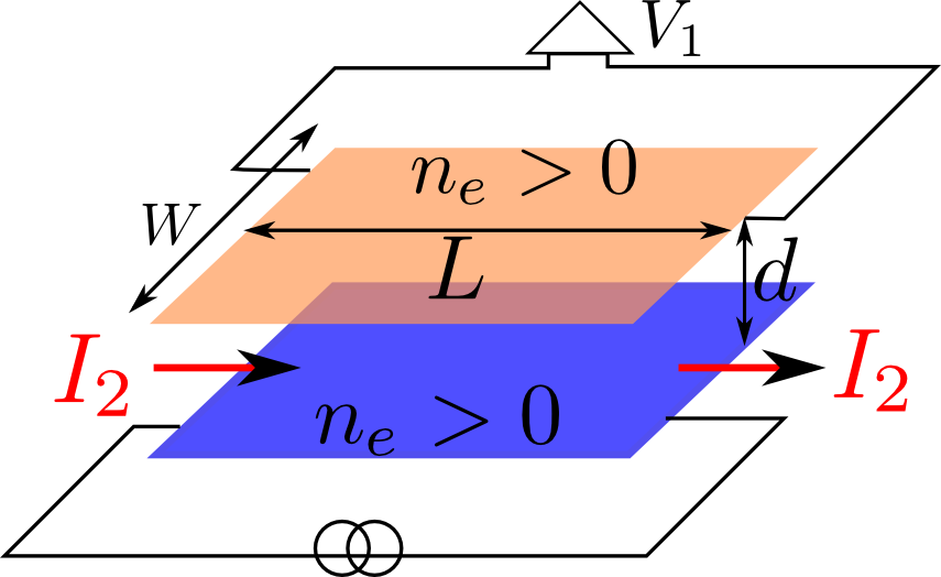
Using the above equations we can eliminate the trans-conductivity in terms of and rewrite the relationship between the drag and the longitudinal resistivities as:
| (4) |
where . Eq. (4) has two extreme limits:
| (5) |
Hence, in the limit where the drag resistivity is small compared with the resistivity of the two layers () the longitudinal resistivity is dominated by the resistivity of the active layer. This is the usual case of the 2D electron gases (2DEG), found in semiconducting heterostructures [2, 3, 4], where the drag resistance is a small effect.
In what follows, we will argue that for the case of an ultra-clean graphene double layer the opposite regime can be reached, namely, one can have with so that the longitudinal resistivity, , is proportional to the drag resistivity, but enhanced by a factor proportional to , so that . This regime can be reached in ultra-clean graphene by tuning the bottom and top gates in the device (see Fig. 1) such that the Fermi energy of the non-active layer, (where m/s is the Fermi velocity), is large, but the Fermi energy of the active layer, , is small and close to the neutrality point (that is, one requires that ). This is only possible in graphene because the resistivity in each individual graphene layer is a monotonically decreasing function of the density, , in each plane () [5]. In ultra-clean graphene, the resistivity is a very sharp function of the density and therefore the longitudinal resistivity can be enhanced by orders of magnitude by the drag effect. In fact, we show that the drag resistance diverges at low densities as () and therefore the longitudinal resistance can become arbitrarily large. We stress that the behavior for , as computed using our model, is better described by the relation , where the exponent is a function of and shows a crossover from to as decreases.
The mechanism described here can produce a huge enhancement of the on-and-off ratio for current flow in graphene, without the need for the opening of a gap in the spectrum, solving the famous bottleneck for the use of graphene devices in high end electronic applications.
While we wait for the drag data in ultra-clean samples [6], we check our model against the existing data for drag resistivity measurements in graphene on SiO2 [7]. As it is well known, SiO2 is a dirty substrate, and at low densities electron-hole puddles are formed [8, 9], greatly limiting the mobility in these devices. We show that our model applies to this conventional case describing the data extremely well.
We notice that the theoretical literature on Coulomb drag in graphene is scarce [10, 11], and it was shown [7] that the theoretical approaches used so far [10, 11] are unable to describe the experimental data. Under a number of simplifying assumptions, it was shown [11] that electrons in graphene, when described by the massless Dirac equation, should have zero drag-resistivity. According to that analysis [11], trigonal warping corrections would be necessary to explain a finite drag resistivity in graphene. We show here that such is not the case when the momentum dependence of the scattering time is taken into account and dynamic effects in Coulomb screening are correctly included.
2 Theory of Coulomb drag and experimental results
The drag resistivity can be obtained from the solution of Boltzmann’s kinetic equation [12, 13, 14, 15, 16]. In this approach it is assumed that the main scattering mechanism within a graphene layer is electron-impurity scattering [17, 18] and that the electronic density is outside the range where one finds electron-hole puddles[8, 9]. In dirty substrates such as SiO2 this can happen at densities of 1012 cm-2, however, in cleaner substrates such as Boron-Nitride [19] this only happens at extremely low densities of the order of 1010 cm-2 [20]. Without loss of generality we also assume that the graphene layers are electron doped and, as explained above, the Fermi energy in the two graphene layers is such that . We also make use of the full dynamical screening between the layers, which takes into account intra- as well as inter-layer interactions. However, in calculating the resistivity we only take into account intra-band interactions between electrons belonging to each of the sheets (the validity of this assumption is achieved by keeping the electronic density large enough [11]). Finally, one key point of our approach is taking into account the full momentum dependence of the electronic scattering time , originated from electron-impurity scattering. It is well known that is roughly proportional to the square root of the electronic density, that is, we have , where is a constant computed elsewhere [17], and which drops out at the end of the calculation. This assumption is in agreement with the experimental data [5] and is essential for the accurate description of Coulomb drag in graphene.
Within these assumptions, Boltzmann’s kinetic equation suffices for the description of the drag resistivity. The final result for the latter quantity (and the central result of this paper; see derivation ahead) is
| (6) | |||||
The reader is referred to the derivation of Eq. (24) for the definition of the several quantities in Eq. (6). Using Eq. (6) we are able to describe quantitatively the drag resistivity measured in graphene at different temperatures [7]. Our results are summarized in Fig. 2.
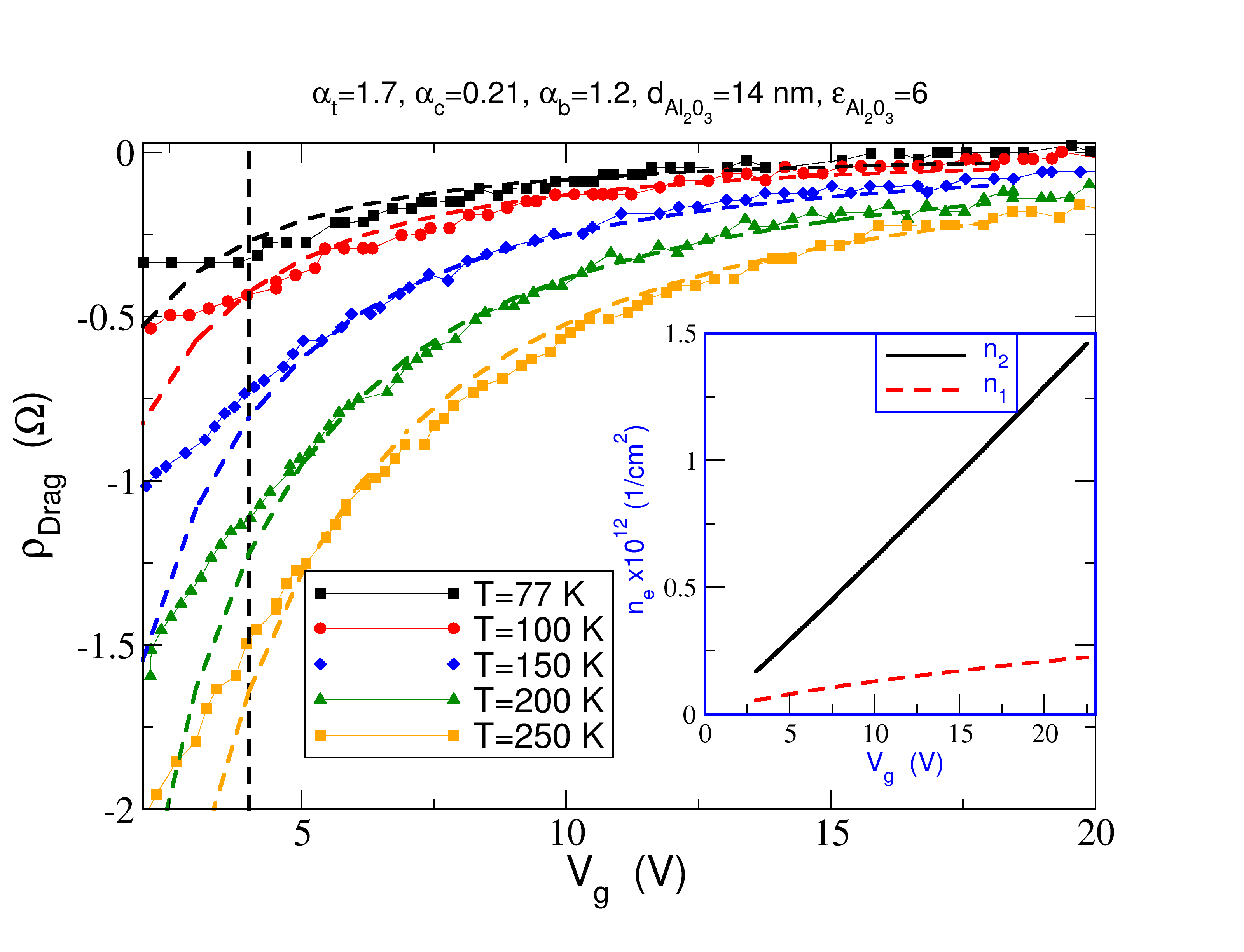
In that figure the symbols are the experimental data and the dashed lines are the calculated values of . The drag resistivity is represented as function of the gate voltage. The calculated curves have been horizontally shifted by V, since the graphene in the device had its neutrality point at , whereas the calculated curves assume neutral graphene when . The agreement is quantitative up to ; below we discuss the origin of the deviations for V, which are associated with the electron-puddle formation in the device. To understand the experimental conditions associated with the measurements reproduced in Fig. 2 the reader is referred to Ref. [7].
The device has two different dielectrics: SiO2 (relative permittivity ), with thickness nm, and Al2O3 (relative permittivity [21]), with thickness nm (we note that other authors report a value of [22]). The latter oxide is sandwiched between the two graphene layers. As detailed in Ref. [7], the densities in the two layers are not independent of each other. The electronic densities and follow from [7]:
| (7) | |||||
| (8) |
The numerical solution of the last two equations gives the electronic density in the two graphene sheets for any value of (see inset in Fig. 2).
In our theory, the only free parameter is the intrinsic dielectric of constant graphene or, equivalently, the interaction parameter:
| (9) |
We note that there is some controversy on the value of [23]. When graphene is immersed in a dielectric of relative permittivity , the interaction parameter becomes . In the experimental setup [7] there are three different interaction parameters: two associated with electron-electron interactions within the two graphene planes ( and ) and one associated with the inter-plane interaction (). The constants and play their role in the calculation of the dielectric function of the coupled layers. Explicitly, we have:
| (10) | |||||
| (11) | |||||
| (12) |
Taking as reference, we get and ; these two numbers are fixed in our model. Therefore, the only free parameter is , or in alternative . We have chosen as our fitting parameter and the best fit was obtained for . This latter value implies:
| (13) |
a number close to the one given by Eq. (9).
The vertical dashed line in Fig. 2 sets the limit of validity of our theoretical model in what concerns its application to graphene on dirty substrates. Indeed, at that point the experimental curves change their curvature from negative to positive, indicating a change of regime. Below V, the theoretical results start to deviate from the measured data. This happens because the electronic density in the bottom layer approaches the regime where electron-hole puddles control the electronic transport in graphene [7]. In fact, looking at the green curve of Fig. 3.a in Ref. [7], we see that during the transition from the regime of electron-electron drag to that of electron-hole drag the behavior of is reminiscent of that reported for Hall-measurements in graphene close to the neutrality point [5]. In both cases, the elementary theory, which ignores the effect of electron-hole puddles, predicts diverging drag resistivity and Hall coefficient. We note that our computed curves diverge as the electronic density is reduced; the divergence is enhanced at high temperatures. In the absence of electron-hole puddles can become large, giving rise to the switching effect we have described in the introduction.
3 Derivation of the drag resistivity formula
The calculation of the current density (the driven current) and the electric field (the drag field) requires the solution of Boltzmann’s equation, under the assumption that the current density in sheet 1 is zero, . The driven current reads
| (14) |
Following a standard procedure [14, 15, 16], the drag field is given by:
| (15) |
where is the collision integral due to inter-plane Coulomb interactions, is the charge of the carriers in plane 1, , is the electronic density in layer 1, and and are the spin and valley degeneracy, respectively. We stress that unlike previous works [10] we take fully into account the momentum dependence of the relaxation time. It was noted before that ignoring this momentum dependence leads to incorrect results [16] (for the 2DEG, however, the relaxation time can be taken momentum independent).
The calculation of the collision integral requires the use of the Coulomb interaction between electrons in different layers. The latter is given by
| (16) | |||||
where the creation operators and refer to electrons in layers 1 and 2, respectively, is the area of the system, and
| (17) |
where is the inter-layer distance. The transferred momentum between the layers is , refer to the valence ( or -1) and conduction ( or +1) band electrons, the momentum of electrons in plane 1 is denoted by and for electrons in plane 2 by ; the momentum sums and contain spin summations as well. The chiral nature of the electron wave function is encoded in the form factors:
| (18) | |||||
| (19) |
where .
Following a standard approach [24, 14, 15, 16], we have
| (20) |
where is the dynamic Coulomb interaction, evaluated using the random phase approximation for the dynamic dielectric function . We note that is not the relaxation time (see above), and it cancels out when the ratio is computed. We also have
| (21) |
where , (), and the function , with , is defined as
| (22) | |||||
The difference between our calculation and that of Tse et al. [10] is precisely in the form of the . The dynamic dielectric function for the two-layer system is given by [16, 25]:
| (23) |
where and are the dielectric and polarization functions of each of the individual layers [26]. Notice that and enter in and , respectively. Once the functions are computed, a relatively simple expression follows for the drag resistivity:
| (24) |
which leads to Eq. (6) and is the interaction parameter of graphene considering the dielectric in between the two graphene layers made out of Al2O3.
The dimensionless function is defined as:
| (25) |
where
| (26) |
and and are dimensionless variables defined as and , respectively. The three integration regions are: , ; , ; , where and . The function is defined as:
| (27) | |||||
where
| (28) |
and equals or , depending on the graphene layer. Below we outline the calculation of the functions .
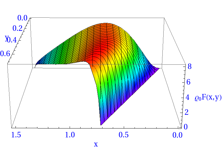
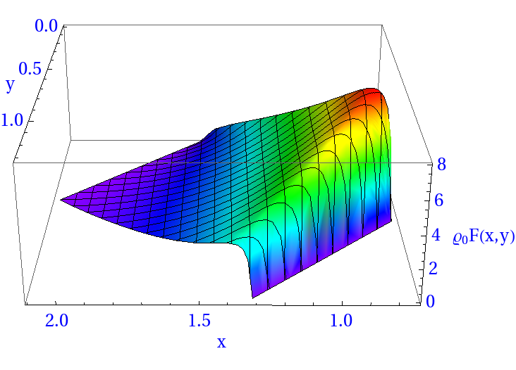
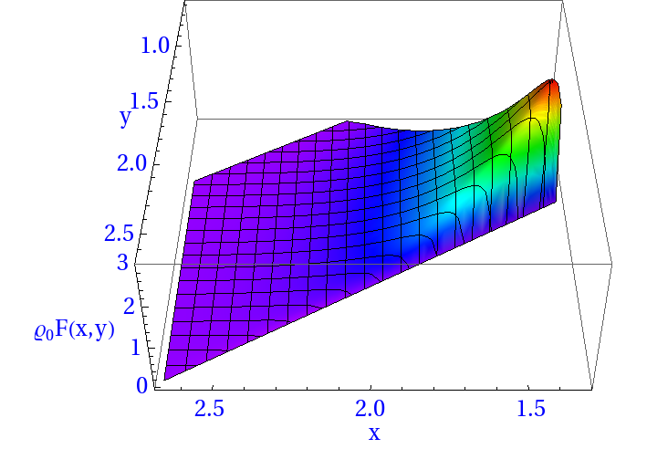
In Fig. 3 we plot the quantity for particular values of (as determined by the gate voltage), the effective interaction parameter , the distance between the two layers, and the temperature. In that figure the three panels, from top to bottom, represent the contribution of the three integration domains defined by and . At low temperatures and high back-gate voltage, only the contribution of region is significant; on the other hand, at high temperature and low densities all the three regions () give a significant contribution to , as shown with the example in Fig. 3.
4 Particular limits of
Let us now consider the case where , , and are all equal, as is the electronic density in the two sheets. Taking the limit of very low densities, we see that can reach values of the order of , as in the case represented in Fig. 4.
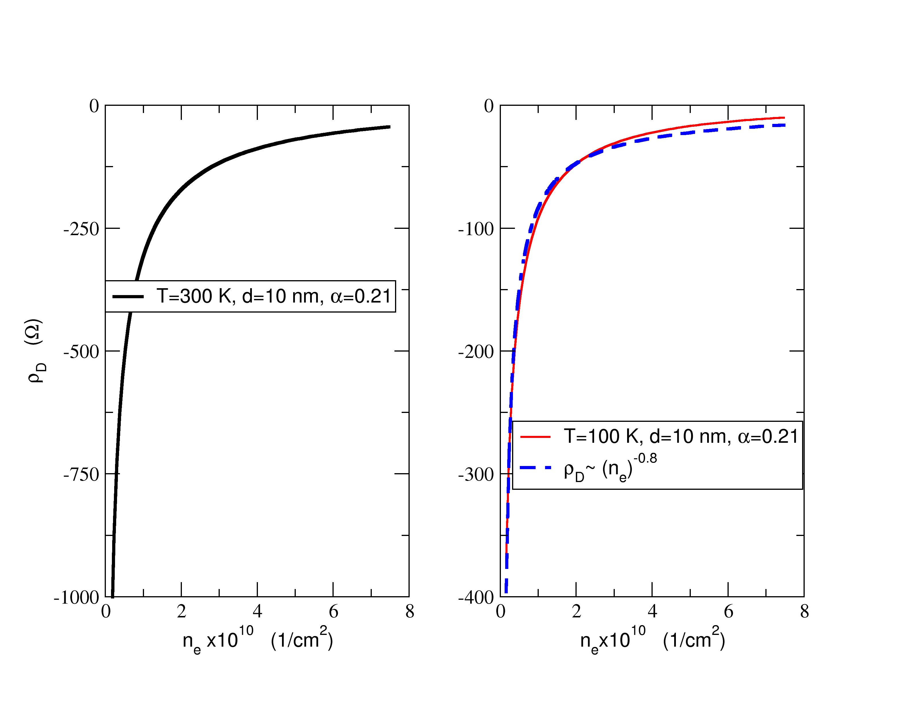
It is the possibility of having large values of that suggests the mechanism for turning on-and-off the electric current in a double-layer graphene-based transistor. We also note that in the density range cm-2 to cm-2, is better described by , where the exponent shows a crossover from to as the electronic density is reduced.
Finally, when and , the asymptotic regime for reads
| (29) |
The asymptotic formula (29) has a different dependence on and from that found in Ref. [10], due to the inclusion of the momentum dependence in the scattering time; in Ref. [10] the integration over has a kernel of the form , whereas our kernel, in the same limit, has the form . Thus we obtain and Tse et al. have obtained . The difference by a factor of two in the power of the momentum comes from: (i) ; (ii) appears twice in the right-hand side of Eq. (15). It is worth stressing that Eq. (29) does not apply to the conditions of the experiment we have described in Fig. 2, and the experimental conditions where it would apply can hardly be reached. Also, the values of of an experiment done in the regime of validity of Eq. (29) would be difficult to measure.
5 Technical details: Calculation of the functions at zero temperature
The functions – – depend on the integration limits and – ; we also define . We write , where
| (30) |
At zero temperature we have:
| (31) |
In terms of the functions and , the function reads:
-
1.
region 1: and , in which case we have (we have omitted the arguments of the functions for the sake of simplicity);
-
2.
region 2: and , in which case we have ;
-
3.
region 3: and , in which case we have ;
-
4.
region 4: and , in which case we have .
In the regions where is finite we have
| (32) | |||||
| (33) |
where and .
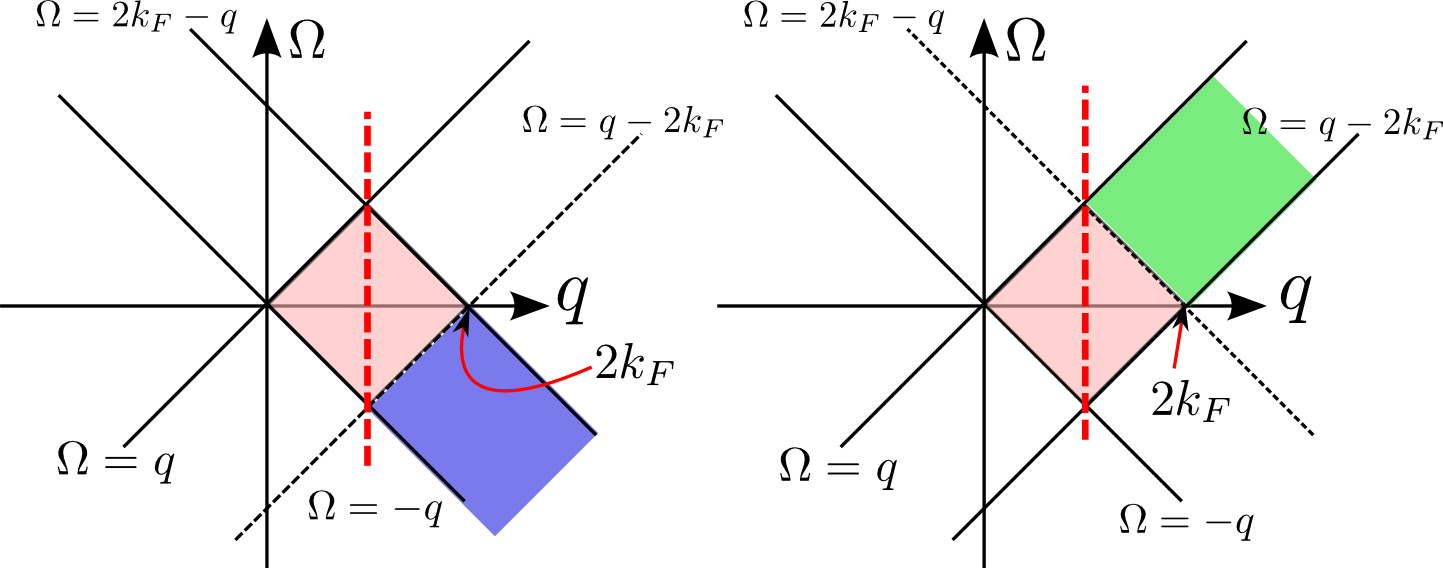
The four regions above have their graphical representation in Fig. 5. In the triangular area of the diagram 5, the polarization reads
| (34) |
In the rectangular area of the same diagram, the polarization is obtained by adding to Eq. (34) the term
| (35) |
where and
| (36) | |||||
| (37) |
We have used these results for the polarization in the calculation of the dynamic dielectric function.
6 Conclusions
We have given a quantitative theory of Coulomb drag in graphene. We have shown that for ultra-clean graphene, unlike the case of a conventional 2DEG, can be tuned to a region of diverging drag and longitudinal resistivity allowing the use of double layer structures for device applications where the on-and-off ratio for the current flow has to be large. We also show that our theory explains quantitatively the experimental data for the drag resistivity in dirty devices away from the electron-hole puddle region. As this region shrinks in cleaner devices, the validity of our theory extends.
7 Supplementary Information
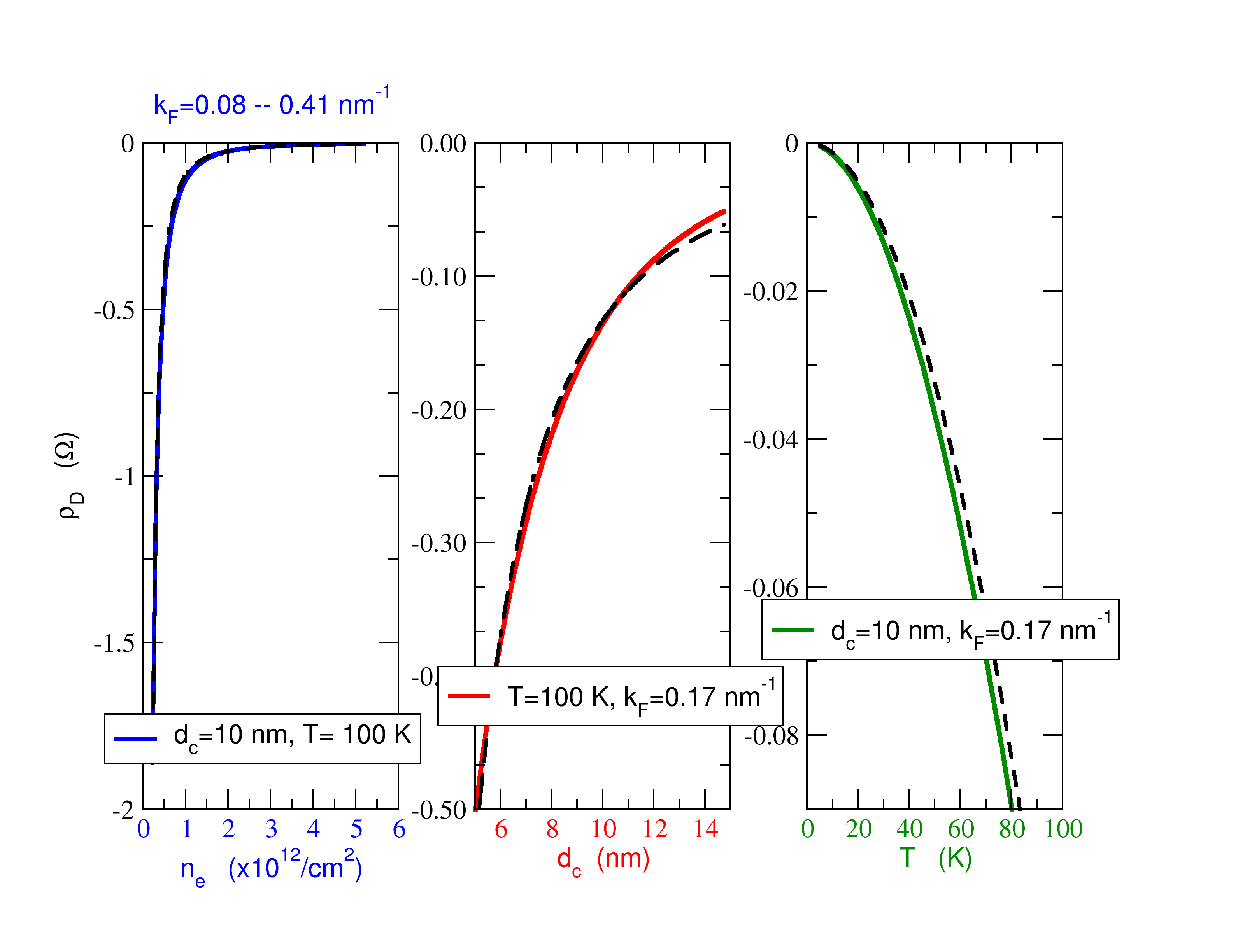
In Fig. 6 we plot the dependence of the drag resistivity as function of the electronic density, , the interlayer distance, , and the temperature, . The density range scanned in this figure is different from that given in Fig. 4. In the three panels of Fig. 6 the black dashed lines are fits to a power law of the form , where represents one of three parameters , , and . From these fits we have found that follows, in the regime of parameters of Fig. 6, roughly the behavior
| (38) |
It is also clear from Fig. 6 that Eq. (38) holds only approximately. Also, comparing the dependence of on , as given in the regime of parameters of Fig. 4, with that of Eq. (38), obtained from Fig. 6, we see that the exponent changes with density, being smaller at smaller density values.
8 Acknowledgments
We thank useful discussions with A. Geim and K. Novoselov. AHCN acknowledges DOE grant DE-FG02-08ER46512 and ONR grant MURI N00014-09-1-1063.
References
- [1] \NameRojo A. G. \REVIEWJ. Phys.: Condens. Matter 111999R31.
- [2] \NameSolomon P. M., Price P. J., Frank D. J. La Tulipe D. C. \REVIEWPhys. Rev. Lett. 6319892508.
- [3] \NameGramila T. J., Eisenstein J. P., MacDonald A. H., Pfeiffer L. N. West K. W. \REVIEWPhys. Rev. Lett. 6619911216.
- [4] \NameGramila T. J., Eisenstein J. P., MacDonald A. H., Pfeiffer L. N. West K. W. \REVIEWPhysica B 1971994442.
- [5] \NameNovoselov K. S., Geim A. K., Morozov S. V., Jiang D., Zhang Y., Dubonos S. V., Grigorieva I. V. Firsov A. A. \REVIEWScience 3062004666.
- [6] A. K. Geim, private communication.
- [7] \NameKim S., Jo I., Nah J., Yao Z., Banerjee S. K. Tutuc E. \REVIEWPhys. Rev. B 832011161401.
- [8] \NameMartin J., Akerman N., Ulbricht G., Lohmann T., Smet J. H., von Klitzing K. Yacoby A. \REVIEWNature Phys. 42008144.
- [9] \NameZhang Y., Brar V. W., Girit C., Zettl A. Crommie M. F. \REVIEWNature Phys. 52009722.
- [10] \NameTse W.-K., Hu B. Y.-K. Das Sarma S. \REVIEWPhys. Rev. B 762007081401.
- [11] \NameNarozhny B. N. \REVIEWPhys. Rev. B 762007153409.
- [12] \NameLaikhtman B. Solomon P. M. \REVIEWPhys. Rev. B 4119909921.
- [13] \NameSolomon P. M. Laikhtman B. \REVIEWSuperlattices and Microstructures 10199189.
- [14] \NameJauho A.-P. Smith H. \REVIEWPhys. Rev. B 4719934420.
- [15] \NameFlensberg K. Hu B. Y.-K. \REVIEWPhys. Rev. Lett. 7319943572.
- [16] \NameFlensberg K. Hu B. Y.-K. \REVIEWPhys. Rev. B 52199514796.
- [17] \NamePeres N. M. R. \REVIEWRev. Mod. Phys. 8220102673.
- [18] \NameAbergel D. S. L., Apalkov V., Berashevich J., Ziegler K., Chakraborty T. \REVIEW592010261
- [19] \NameDean C. R., Young A. F., Meric I., Lee C., Wang L., Sorgenfrei S., Watanabe K., Taniguchi T., Kim P., Shepard K. Hone J. \REVIEWNature Nanotechnology 52010722.
- [20] \NameDas Sarma S. Hwang E. H. \REVIEWPhys. Rev. B 832011121405.
- [21] \NameKim S., Nah J., Jo I., Shahrjerdi D., Colombo L., Yao Z., Tutuc E., Banerjee S. K. \REVIEWAppl. Phys. Lett. 942009062107.
- [22] \NameLiao L., Bai J., Qu Y., chen Lin Y., Li Y., Huang Y. Duan X. \REVIEWPNAS 10720106711.
- [23] \NameReed J. P., Uchoa B., Il Joe1 Y., Gan Y., Casa D., Fradkin E. Abbamonte P. \REVIEWScience 3202010805.
- [24] \NameZiman J. M. \BookPrinciples of the Theory of Solids 2nd Edition (Cambridge University Press) 1979.
- [25] \NameUchoa B. Castro Neto A. H. \REVIEWPhys. Rev. Lett. 982007146801.
- [26] \NameWunsch J. B., Stauber T., Sols F. Guinea F. \REVIEWNew J. Phys. 82006318.