Electron dynamics in topological insulator semiconductor-metal interfaces (topological p-n interface)
Single-Dirac-cone topological insulators (TI) are the first experimentally discovered class of three dimensional topologically ordered electronic systems, and feature robust, massless spin-helical conducting surface states that appear at any interface between a topological insulator and normal matter that lacks the topological insulator ordering Intro ; TIbasic ; DavidNat1 ; DavidScience ; DavidTunable ; MatthewNatPhys . This topologically defined surface environment has been theoretically identified as a promising platform for observing a wide range of new physical phenomena, and possesses ideal properties for advanced electronics such as spin-polarized conductivity and suppressed scattering DavidScience ; dhlee ; MacDonaldKerr ; FuNew ; FerroSplitting ; FuHexagonal ; TopoFieldTheory ; Biswas ; ExcitCapacitor ; palee ; ZhangDyon ; KaneDevice ; DavidNat1 ; MatthewNatPhys ; ZhangPred ; DavidTunable ; YazdaniBack ; WrayCuBiSe ; WrayFe ; YeHelix . A key missing step in enabling these applications is to understand how topologically ordered electrons respond to the interfaces and surface structures that constitute a device. Here we explore this question by using the surface deposition of cathode (Cu/In/Fe) and anode materials (NO2) and control of bulk doping in TI Bi2Se3 from P-type to N-type charge transport regimes to generate a range of topological insulator interface scenarios that are fundamental to device development. The interplay of conventional semiconductor junction physics and three dimensional topological electronic order is observed to generate novel junction behaviors that go beyond the doped-insulator paradigm of conventional semiconductor devices and greatly alter the known spin-orbit interface phenomenon of Rashba splitting. Our measurements for the first time reveal new classes of diode-like configurations that can create a gap in the interface electron density near a topological Dirac point and systematically modify the topological surface state Dirac velocity, allowing far reaching control of spin-textured helical Dirac electrons inside the interface and creating advantages for TI superconductors as a Majorana fermion platform over spin-orbit semiconductors.
The surface state of topological insulator Bi2Se3 crystals cleaved in ultra high vacuum (UHV) is a singly degenerate Dirac cone that spans a bulk semiconductor band gap of 300meV DavidTunable ; MatthewNatPhys ; ZhangPred ; WrayCuBiSe , with a Fermi level that can be easily moved by bulk dopants (Fig. 1a). These surface electron dynamics, identified in 2008, have inspired an ongoing stream of proposals anticipating new phenomena and technologies that can be achieved by interfacing conventional electronics with two dimensional spin-chiral Dirac electrons, including the possibility of observing exotic quasiparticles such as Majorana fermions, dyons and axions with properties that have been found nowhere else in the universe FuNew ; ZhangDyon ; TopoFieldTheory . Developments from the last few months have demonstrated that it is possible to fabricate nanodevices using Bi2Se3 and pass current through the surface states topGate ; sacebeDevice , but have also highlighted the fact that topological insulators are a new state of matter distinct from normal metals and insulators, and their properties in a junction setting are not yet known. Changes in the surface chemistry of Bi2Se3 have been found to modify the Dirac cone kinetics in unpredictable ways WrayCuBiSe and induce bulk electrons to be trapped in new surface Dirac cones WrayFe . To bridge the gap between the conceptual promise of topological insulator Dirac electrons and real devices that can take advantage of topological electronic order, it is critical to develop an experimentally motivated understanding of how interfaces between normal metals and topological insulators will function.
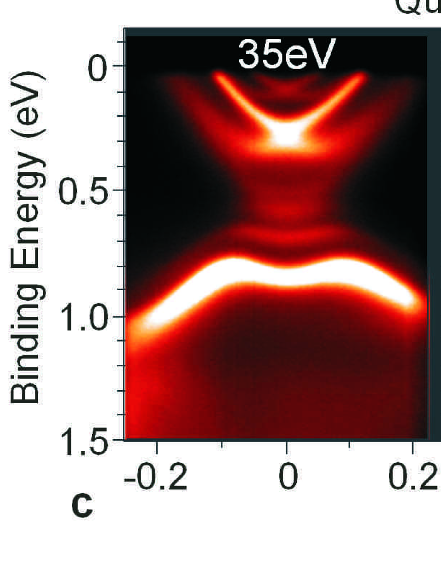
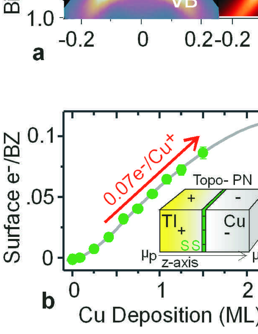
To determine how junctions will change the topological electron kinetics, we have deposited thin films on the surface of carrier doped Bi2Se3 to generate a wide range of semiconductor-metal P-N and N-N interfaces, and used angle resolved photoemission spectroscopy (ARPES) to map changes in the topological surface electrons. The non-TI part of the interface is grown by evaporative deposition of strong charge donors (Cu, NO2, Fe), achieving conventional diode interface voltages up to Vd0.7eV from a sub-nanometer surface layer that is permeable to photoexcited electrons univCurve . The cleaved Se2- plane of Bi2Se3 is maintained at low temperature (T20oK) to provide a chemically neutral and homogeneous surface for these adatoms, as discussed in the online Supplementary Information (SI). Deposition depth is presented in units of monolayers (ML) to approximately represent the number of deposited ions per hexagonal unit cell of the surface, based on rough linear assumptions outlined in the SI. Summing the Fermi surface area of all surface states gives the surface state electron density or Luttinger count, which we find grows more slowly than the nominal rate of charge deposition with Cu+ or Fe (Fe2+ or Fe3+) ions by approximately one order of magnitude. After an estimated 2ML of Cu deposition the Fermi level ceases to move as more adatoms are deposited, and very few additional electrons can be added to the surface states (Fig. 2b). As shown in Fig. 1c, the topological surface state is dramatically changed by the voltage drop in a P-N inteface between hole doped (P-type) Bi2Se3 and copper, manifesting new Dirac cones and a gap in the surface density of states near the original (D0) Dirac point at 0.6-0.7eV binding energy.
The observation of a gap in the surface electron density is extremely surprising, because it is well known from theory that non-magnetic perturbations cannot open a true band gap in topological surface state Dirac points Intro ; TIbasic . To understand how the junction with non-magnetic copper could cause such a feature to appear, we have created a Green’s function implementation of the experimentally-based kp model in Ref. FuNew ; FuHexagonal to numerically simulate junctions at the surface of a semi-infinite topologically ordered Bi2Se3 slab based on experimentally measured bulk electron kinetics from Ref. WrayCuBiSe ; fisherBending . Unlike other current numerical models, this approach is capable of simulating the full screening depth of electrostatic interactions inside a Bi2Se3 junction (100nm), and encompasses both the experimentally determined bulk kinetics and the underlying topological order of electrons in the simulated crystal. Using a screening potential that matches the observed change in topological surface state electron energies in the Bi2Se3-Cu P-N interface (=0.7eV), the simulation shows that the upper Dirac cone surface state electrons are still found in the first quintuple atomic layer of Bi2Se3, but the corresponding lower Dirac cone electrons are found more than 1nm deeper in the crystal, due to hybridization with other surface states derived from the perturbed bulk valence band (Fig. 1b). Because the lower Dirac cone electrons of the original surface state are deeper in the crystal than the 1nm photoemission penetration depth, photoemission measurements are expected to show a void or “gap” near the D0 Dirac point, even though the three dimensional band structure is not gapped. This effect observed from our data and model is consistent with a recent theoretical proposal that interfacing TI surface states with a parasitic (degenerate) 3D metal can reshape the surface bands to take the appearance of a band gap parMetal , a coexistence expected in many theoretically predicted topologically ordered metals such as half-Heusler compounds HeuslerDiscovery .
The incremental evolution leading to the appearance of multiple new Dirac cones on Cu-deposited P-type Bi2Se3 is shown in Fig. 2. The build-up of positively charged surface ions first donates electrons to the original Dirac cone of freshly cleaved Bi2Se3, and then gradually binds four new surface states that intersect in two new Dirac points (D1 and D2) at the Brillouin zone (BZ) center. Tracing these new states from their points of intersection in the BZ center, we observe that they exchange partners and merge with a different surface band at momenta larger than 0.1, corresponding roughly to the outer contour of the region in which symmetries are inverted to bring about the TI state in numerical models. The resulting Fermi surface after heavy deposition (Fig. 2a, right) is made up of three rings, of which the outer two are doubly degenerate (within intrinsic width resolution). The doubly degenerate outer rings cannot carry a non-zero Berry’s phase, meaning that the Berry’s phase of by which a topological insulator interface is identified is obtained from the innermost singly degenerate Fermi surface ring, located deepest inside the Bi2Se3 crystal. The outermost ring is found at k1.7-2.0, and is hexagonally warped into a doubly-degenerate “snowflake” shape that resembles the singly degenerate hexagonal Fermi surface associated with magnetic instabilities in related Bi2Te3 FuHexagonal . Although alternative terminologies have been proposed in recent literature HofmannRashba2DEG , we refer to all of these surface bands as topological surface (or interface) states, because they manifest at the surface of the material and all five Dirac bands must be observed to measure the = topological Berry’s phase.
In topologically trivial semiconductors with strong spin-orbit interactions, electrons near an interface are commonly spin-split into spin polarized Dirac cones by the Rashba effect. The partner swapping behavior we observe in the D1 and D2 Bi2Se3-Cu P-N interface states appears identical to the conventional Rashba effect in photoemission measurements at small momenta (K0.1), but has very different phenomenological implications. The conventional Rashba effect causes surface electrons to be more strongly spin-polarized as their momentum deviates from the BZ center, due to the Rashba Hamiltonian term which is proportional to momentum (R=(2, with representing spin). In contrast, though Bi2Se3-Cu P-N interface electrons obey this linear relation near their Dirac points, at large momentum the surface electrons are all nearly doubly-degenerate, and do not generate a large density of spin-polarized conduction states at the Fermi level. The difference can be seen clearly by comparing the Bi2Se3-Cu interface band structure with the surface states of BiTeI (Fig. 2c), a compound chemically similar to Bi2Se3, but which our measurements show to be topologically trivial and have an extremely strong Rashba effect (=2.20.1eV*, see SI). Due to the partner swapping effect, spin-helical conduction states inside the interface are still limited to a single Dirac cone as is desired for applications.
The upper Dirac cone surface state of the N-type Bi2Se3 samples explored in this study (including CuxBi2Se3) has a momentum-axis width (k) of k0.035 at half maximum intensity before deposition, which can be inverted to reveal the electronic mean free path (mfp) of =1/k=29. Momentum-axis width of the original Dirac cone increases steadily as Cu is added to the surface (Fig. 2d) and is surprisingly broad when one considers that disorder-induced scattering is suppressed by the spin-momentum locking of electrons DavidScience ; DavidTunable ; YazdaniBack . Depositing magnetic iron ions instead of non-magnetic copper results in an unusual fluctuation in k that has been discussed in Ref. WrayFe and may be due to reduced disorder following a 2D ferromagnetic ordering transition. The new surface states generated by copper deposition have sharper momentum widths of 0.0273 (=37 mfp) just above the 0.27eV binding energy D1 Dirac point in Fig. 2a(right) and 0.0233 (=43 mfp) just above the 0.1eV D2 Dirac point. The capability to generate a longer mean free path of spin polarized surface electrons via deposition or top gating, as identified in Fig. 2, is desirable to enhance long range magnetic FuHexagonal ; WrayFe ; YeHelix and non-Abelian coherent behaviors unique to topological insulators WrayCuBiSe ; FuNew .
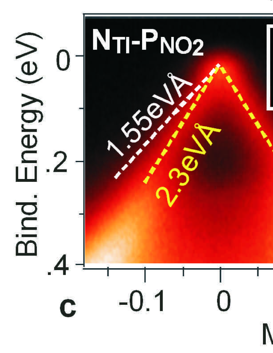
Topological insulators are among the very few material systems with band structures that can be manipulated to achieve transport defined by a Dirac point DavidTunable , and most proposed applications for TIs derive from the behavior of low density spin-helical Dirac surface electrons. In Fig. 3c we present two realizations of P-N interfaces in which the Bi2Se3 surface state Dirac point is brought to the Fermi level where it will shape transport properties. The surface chemical potential of the N-type sample shown at left (as-grown Bi2Se3 with [Se]2+ defects) is lowered by depositing NO2-, and the P-type sample (Bi1.995Ca0.005Se3) was modified through deposition of In+. Our data show that lowering the surface chemical potential of an N-type sample to the Dirac point has the effect of dramatically increasing the Dirac velocity from vD=1.550.08eV to 2.300.08eV, observed from the lower Dirac cone band slope traced in Fig. 3a,c. The velocity of lower Dirac cone electrons changes rapidly immediately after deposition begins, but stabilizes after the surface chemical potential falls below the bulk conduction band minimum 0.170.02 eV above the Dirac point (Fig. 3b). When the chemical potential lies inside the bulk electronic gap as measured by surface-sensitive photoemission, the lower Dirac cone velocity has the same value of 2.30.1eV for both N-type and P-type samples (Fig. 3b,c) even though the they are exposed to surface ions with opposite charge. As the chemical potential at the surface of Bi2Se3 is bent into the bulk band gap, numerical simulations show that the region near the surface becomes depleted of bulk conduction electrons (Fig. 3d and Fig. S5 in the SI), causing bulk and surface charge carriers to no longer spatially overlap with one another. The bulk and surface charge carriers occupy the same atomic orbitals, and spatial overlap between the surface and bulk conduction electrons will result in strong on-site charge and spin interactions that are likely responsible for the tunable Dirac velocity observed in our data.
Interfaces with like carrier type (N-N or P-P) are also of great technological importance, because they create a less resistive electronic junction with minimal charge inhomogeneity. Measurements in Fig. 4 explore the effect of light copper deposition on the surface of N-type Cu0.02Bi2Se3 to observe how an N-type surface layer interfaces with the electron doped topological insulator. Excess surface-deposited Cu adatoms cause the electron energies near the surface of the TI to bend towards higher binding energy, as they would in an N-N Schottky diode. A new surface state is fully formed after 0.08ML of Cu deposition (Fig. 4a, measurements at 0.08ML coverage in SI), and remains doubly degenerate within experimental resolution until approximately 0.15ML of Cu deposition, at which point it becomes spin-split as seen from a deviation between the band energy at the Brillouin zone center and the band energy minimum (Fig. 4c).
Because TI surface states cross the bulk band gap and have different energetics than bulk electrons TIbasic ; DavidScience , when interfacing non-TI materials with a topological insulator, the surface states will trap charge carriers and attract or repel bulk electrons even when the bulk carrier doping of each material is identical. Our ARPES measurements show that prior to depositing ions on the vacuum-cleaved Cu0.02Bi2Se3 surface, a negative charge is trapped by the surface state, and will be screened over a range of more than 10 nanometers as simulated from the Poisson equation (Fig. 4e). Assuming that each Cu atom enters a +1 valence state, depositing 0.08ML of copper causes the net charge at the crystal surface to change from negative to positive. Between 0 and 0.08ML (shaded in Fig. 4e) the electric field penetrating beyond the first few nanometers of the crystal surface is expected to be very small, allowing electrons to retain their bulk-derived energetics and symmetries as they approach the surface from deeper in the crystal. As Cu deposition is raised to 0.16ML, electron density in the surface state grows more slowly than the rate of deposition, causing an increasing proportion of the surface charge to be screened by bulk electrons. Titrating with positive ions or a gating voltage (0.1eV from our data) to achieve an electrically neutral surface is therefore a promising method to enhance bulk interactions with the surface states, such as magnetic and superconducting proximity effects.
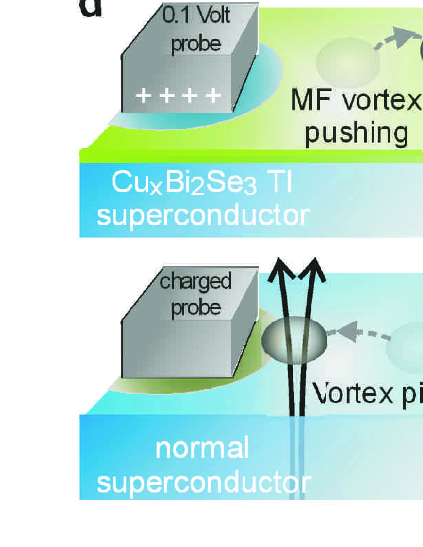
Recent measurements have identified that the bulk doped TI CuxBi2Se3 (x0.1) is a type-2 N-type bulk superconductor (Ref. WrayCuBiSe and Fig. 1a, left), and that magnetic vortices at the surface are likely to bind non-Abelian particles known as Majorana fermions that have not yet been observed in nature WrayCuBiSe ; FuNew . Our calculations in Fig. 4e show that an electric field from the negatively charged surface state will cause rapid phase fluctuations that suppress superconductivity if the surface charge is not neutralized (Fig. 4e, inset). Moreover, because vortices are repelled by regions of high superfluid density, this surface environment provides a new mechanism to control the dynamics of Majorana fermions and potentially observe their non-Abelian properties. For normal superconductors, surface perturbations suppress superfluid density, generating an attractive force that pins vortices in place VortexPin ; VortexPush . For a topological insulator however, our data show that adjusting the surface chemical energy to cancel out the negative surface state charge can enhance superfluid density under a probe, causing surface vortices to be repelled by the probe rather than pinned to it (Fig. 4d).
The control and exclusion of vortices is a subject of active research to improve the properties of superconductors VortexPush ; KaneDevice , and the intrinsically charged TI surface provides a new and promising platform for vortex manipulation. Taken collectively, the P-N and N-N interface electronic structures observed here reveal how interface effects such as Rashba spin-splitting and the superconducting proximity effect are changed by the presence of topological order, and how topological insulator interfaces can be tuned to adjust the average speed of surface Dirac electrons and interact with surface Majorana fermion vortices.
Methods summary: Angle resolved photoemission spectroscopy (ARPES) measurements were performed at the Advanced Light Source beamlines 10 and 12 using 35.5-48 eV photons with better than 15 meV energy resolution and overall angular resolution better than 1 of the Brillouin zone (BZ). Samples were cleaved and measured at 15oK, in a vacuum maintained below 810-11 Torr. Fe atoms were deposited using an e-beam heated evaporator at a rate of approximately 0.1/minute, and Cu atoms were deposited at a rate of 0.4/minute. A quartz micro-balance supplied by Leybold-Inficon with sub-Angstrom sensitivity was used to calibrate the deposition flow rate, and a factor of 2.5/ML was used to estimate monolayer depth. Surface charge is estimated from the expected +1 ionization state of copper on the cleaved [111] Se surface WrayCuBiSe . Adsorption of NO2 molecules on Bi2Se3 was achieved by controlled in situ exposures under static flow mode, with care to minimize photon exposure of the adsorbed surface. Crystal growth of large single crystals of CaxBi2-xSe3 and CuxBi2Se3 and numerical techniques used to simulate the perturbed TI surface are described in the SI.
References
- (1) [
- (2) Hasan, M.Z. Kane, C.L. Topological insulators. Rev. Mod. Phys. 82, 3045-3067 (2010).
- (3) Fu, L., Kane, C.L., Mele, E.J. Topological insulators in three dimensions. Phys. Rev. Lett. 98, 106803 (2007).
- (4) Hsieh, D. et al. A topological Dirac insulator in a quantum spin Hall phase. Nature 452, 970-974 (2008).
- (5) Hsieh, D. et al. Observation of unconventional quantum spin textures in topological insulators. Science 323, 919-922 (2009).
- (6) Hsieh, D. et al. A tunable topological insulator in the spin helical Dirac transport regime. Nature (London) 460, 1101-1105 (2009).
- (7) Xia, Y. et al. Observation of a large-gap topological-insulator class with a single Dirac cone on the surface. Nature Physics 5, 398-402 (2009).
- (8) Lee, D.-H. Surface States of Topological Insulators: The Dirac Fermion in Curved Two-Dimensional Spaces. Phys. Rev. Lett. 103, 196804(2009).
- (9) Tse, W.-K. MacDonald, A.H. Giant Magneto-Optical Kerr Effect and Universal Faraday Effect in Thin-Film Topological Insulators. Phys. Rev. Lett. 105, 057401 (2010).
- (10) Fu, L. Berg, E. Odd-parity topological superconductors: theory and application to CuxBi2Se3. Preprint at http://arxiv.org/abs/0912.3294 (2009).
- (11) Garate, I. Franz, M. Inverse spin-galvanic effect in a topological-insulator/ferromagnet interface. Phys. Rev. Lett. 104, 146802 (2010).
- (12) Fu, L. Hexagonal warping effects in the surface states of topological insulator Bi2Te3. Phys. Rev. Lett. 103, 266801 (2009)
- (13) Qi, X.-L., Hughes, T. L. Zhang, S.-C. Topological field theory of time-reversal invariant insulators. Phys. Rev. B 78, 195424 (2008).
- (14) Biswas, R. R. Balatsky, A. V. Impurity-induced states on the surface of 3D topological insulators. Phys Rev B 81, 233405 (2010).
- (15) Seradjeh, B., Moore, J.E. Franz, M. Exciton condensation and charge fractionalization in a topological insulator film. Phys. Rev. Lett. 103, 066402 (2009).
- (16) Law, K. P., Lee, T., Ng, Majorana Fermion Induced Resonant Andreev Reflection. Phys. Rev. Lett. 103, 237001 (2009).
- (17) Qi X.-L. et al. Inducing a magnetic monopole with topological surface states. Science 323, 1184-1187 (2009).
- (18) Fu, L. Kane, C. L. Probing neutral Majorana fermion edge modes with charge transport. Phys. Rev. Lett. 102, 216403 (2009).
- (19) Zhang, H. et al. Topological insulators in Bi2Se3, Bi2Te3 and Sb2Te3 with a single Dirac cone on the surface. Nature Phys. 5, 438-442 (2009).
- (20) Roushan, P. et al. Topological surface states protected from backscattering by chiral spin texture. Nature 460, 1106-1109 (2009).
- (21) Wray, L.A. et al. Observation of topological order in a superconducting doped topological insulator Nature Physics 6, 855-859 (2010).
- (22) Wray, L.A. et al. A topological insulator surface under strong Coulomb, magnetic and disorder perturbations. Nature Physics 7, 32-37 (2011).
- (23) Ye, F. et al. Spin helix of magnetic impurities in two-dimensional helical metal. Europhys. Lett. 90, 47001 (2010).
- (24) Steinberg, H., Gardner, D.R., Lee, Y.S. Jarillo-Herrero, P. Surface State Transport and Ambipolar Electric Field Effect in Bi2Se3 Nanodevices. Nano Letters 10, 5032-5036 (2010).
- (25) Sacepe, B. et al. Gate-tuned normal and superconducting transport at the surface of a topological insulator. Preprint at http://arxiv.org/abs/1101.2352 (2011).
- (26) Seah, M.P. Dench, W.A. Quantitative electron spectroscopy of surfaces - A standard data base for electron inelastic mean free paths in solids. Surf. Interface. Anal. 1, 2 (1979).
- (27) Analytis, J.G. et al. Bulk Fermi surface coexistence with Dirac surface state in Bi2Se3: a comparison of photoemission and Shubnikov-de Haas measurements. Phys. Rev. B 81, 205407 (2010).
- (28) Bergman, D.L. Refael, G. Bulk metals with helical surface states. Phys. Rev. B 82, 195417 (2010).
- (29) H. Lin et al. Half-Heusler ternary compounds as new multifunctional experimental platforms for topological quantum phenomena. Nature Materials 9, 546 549 (2010).
- (30) King, P.D.C. et al. Large tuneable Rashba spin splitting of a two-dimensional electron gas in Bi2Se3. Preprint at http://arxiv.org/abs/1103.3220 (2011).
- (31) Campbell, A.M. Evetts, J.E. Flux vortices and transport currents in type II superconductors. Adv. Phys. 21, 199-428 (1972).
- (32) Villegas, J.E. et al. A Superconducting Reversible Rectifier That Controls the Motion of Magnetic Flux Quanta, Science 302 1188-1191 (2003)