Quantum states and linear response in dc and electromagnetic fields for charge current and spin polarization of electrons at Bi/Si interface with giant spin-orbit coupling
Abstract
An expansion of the nearly free-electron model constructed by Frantzeskakis, Pons and Grioni [Phys. Rev. B 82, 085440 (2010)] describing quantum states at Bi/Si(111) interface with giant spin-orbit coupling is developed and applied for the band structure and spin polarization calculation, as well as for the linear response analysis for charge current and induced spin caused by dc field and by electromagnetic radiation. It is found that the large spin-orbit coupling in this system may allow resolving the spin-dependent properties even at room temperature and at realistic collision rate. The geometry of the atomic lattice combined with spin-orbit coupling leads to an anisotropic response both for current and spin components related to the orientation of the external field. The in-plane dc electric field produces only the in-plane components of spin in the sample while both the in-plane and out-of-plane spin components can be excited by normally propagating electromagnetic wave with different polarizations.
pacs:
73.20.At, 71.70.Ej, 72.25.-b, 78.67.-nI Introduction
It is well-known that the knowledge of a material with high values of spin-orbit (SO) coupling parameters is a goal for many theoretical, experimental, and device research groups in condensed matter physics and spintronics due to its fascinating spin-related properties and possible applications in the information processing and storage. Among the candidates which attract considerable attention throughout the last decade there are Bi/Si(111) surface alloys which band structure has been experimentally studied for several years and recently modeled in a paper FPG by Frantzeskakis, Pons and Grioni. This material, in line with the other examples of ”metal-on-semiconductor” systems with large SO coupling, has been a subject of many both experimental and theoretical papers since it seems very promising to make use of a material combining the large SO splitting of Bi and conventional semiconductor technology of Si which is one of the main goals of spintronics.Awschalom ; Zutic ; Wu Here we shall mention only some of the numerous results of research on the Bi-covered Si surface properties with various crystal orientation of Si substrate. In particular, the scanning tunneling microscopy has been used to determine the surface structure of Bi/Si some 18 years ago, Shioda1993 and the analysis of the atomic geometry and electronic structure continued further Miwa2002 ; Miwa2003 focusing throughout the recent years mainly on the atomic surface geometry and spin-resolved band structure reconstruction where the methods of angle-resolved photoemission spectroscopy have been applied FPG ; Hirahara2006 ; Hirahara2007 ; Hirahara2007b ; Grioni2008 ; Dil2008 ; Gierz2009 ; Bian2009 ; Sakamoto2009 . Other methods included the low-energy electron diffraction and atomic force microscopy Jnawali2006 ; Jnawali2007 , and besides pure Si, the Si-Ge superlattices have been used as a substrate for Bi coverage, Miwa2005 and later the lateral Ge-Si nanostructure prepared on the Si/Bi surface have been studied by the scanning tunneling microscopy.Myslivecek2010 Also, for the Bi/Si system there were studies of energetic stability and equilibrium geometry Miwa2006 and the possibility of designing iron silicide wires along Bi nanolines on the hydrogenated Si surface,Miwa2008 , and of the thermal response upon the femtosecond laser excitation. Hanisch2008 It is well-known that Bi is a material with very big SO splitting, and thus it attracts a steady interest in its potential applications in spintronics where various schemes of combining it with semiconductors are suggested, one of the most recent being an investigation of BiTeI bulk material where the SO splitting reaches a very high value of eV.Nagaosa2011
From the list of papers mentioned above it is evident that the geometric properties of atom arrangement and the resulting band structure have already been studied for Bi/Si systems by many experimental and theoretical groups. However, much lower attention have been given so far to the prediction and observation of different effects caused by the electron system response to an external excitation, including such basic properties as the charge current and spin polarization in the dc field which are often are considered as the starting point of the response calculations, especially for systems with important role of SO coupling.Edelstein1990 ; Aronov1991 ; Kleinert2005 ; Raichev2007 Besides the response to the dc electric field, the optical properties of SO-split band spectrum always attracted significant attention starting from the conventional semiconductor structures with big SO coupling.Bhat2005 ; Sherman2005 ; Tarasenko2005 ; Ganichev2007 ; Berakdar2010 In our previous papers we have observed an important role of SO coupling in conventional InGaAs-based semiconductor superlattices on the energy band formation DK2006 which directly affected both charge and spin response for the excitation by the electromagnetic radiation sooptic ; PSK and by the dc electric field. spinelec It is known that the spin polarization configurations in semiconductors may have a rather long relaxation time Wu ; Pershin2005 ; Stano2006 which makes them as important as the conventional charge current setups for their applications in the nanoelectronics and spintronics.
While there is no doubt that the electron properties in Bi-covered Si interface differ from the ones in conventional semiconductor structures with strong SO coupling, the questions regarding their SO-dependent response to the external dc and electromagnetic fields remain to be very important since we are still in the beginning of our way towards understanding and utilizing such novel materials with giant SO coupling as Bi/Si.
The goal of the present paper is to apply a modified and expanded version of simple but adequate nearly free electron modelFPG for the band structure of electrons in Bi covering the Si(111) surface which allows us to calculate various physical characteristics of this material in the linear response regime, including the charge current and spin polarization caused by dc electric field with different orientations, and also to obtain the response of non-equilibrium spin polarization excited by the electromagnetic field with various polarizations. Indeed, such physical quantities can be among the first ones measured in the nearest experiments on Bi/Si, and hence it is of interest to calculate them beforehand both qualitatively and, when possible, quantitatively. Since we do not know exactly for the present moment many material parameters of the electron system in Bi-covered Si interface, including such parameters as the electron surface concentration and mobility, the dielectric tensor, the relaxation rates for charge and spin, etc, we sometimes cannot yet calculate the effects in the absolute measurable units and use the standard label ”arbitrary units” instead. Still, we believe that the comparison of the output results for the same physical parameter calculated at different conditions always has a value since it allows to predict the relative significance of them when the conditions are varied. We find both common and distinct features of the charge and spin system response in Bi/Si compared to well-known GaAs or InGaAs semiconductor structures. Thus, we believe that our findings can be a good starting point for further theoretical and experimental studies of charge and spin response in Bi/Si system at various external fields.
The paper is organized as follows: in Sec.II we introduce the expanded version of the nearly free electron Hamiltonian for Bi/Si and discuss the band structure and spin polarization in the energy bands, in Sec.III we solve the kinetic equation and calculate the charge current and spin polarization in the dc electric field, in Sec.IV we study the excited spin polarization in the framework of the linear response theory for different polarizations and frequencies of the incident electromagnetic wave, and we give our conclusions in Sec.V.
II Hamiltonian and quantum states
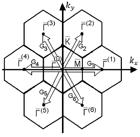
Recent proposal of several theoretical models for band structure calculation of Bi/Si electron surface states FPG provided a variety of choices for studies of the corresponding Hamiltonian and quantum states. Here we shall start with the simplest nearly free electron (NFE) model which was proposed initially for the description of the band structure mainly in the vicinity of the point at the surface Brillouin zone (SBZ) of Bi/Si having a hexagonal shape shown by dashed contour in Fig.1. We shall only briefly describe it here since the detailed derivation and discussion is available in the original paper.FPG The choice of the reciprocal lattice vectors initially has been restricted to three vectors , and connecting four equivalent Gamma-points , , and . In the framework of the NFE approach for each Gamma-point the standard Rashba Hamiltonian of a free electron in the basis has been written with the center of the quasimomentum at the corresponding point. As a result, an matrix is derived giving the energy bands and two-component eigenvectors (the Rashba spinors) describing the spin polarization in the reciprocal space.
We are going to use an expanded version of this model by including the remaining reciprocal vectors , and into our basis of nearest neighbor sites connecting the center Gamma-point with all surrounding points , as it is shown by hollow vectors in Fig.1 where several hexagonal SBZ-s are shown by solid contours, thus creating a Hamiltonian matrix. We assume the previously determinedFPG values of geometrical parameters and . Such an expansion allows us to treat a much wider area of the SBZ compared to the region near the -point FPG and to keep the symmetry of the non-trivial hexagonal Bi/Si(111) trimer structure with one monolayer of Bi atoms.FPG ; Miwa2002 ; Miwa2003 ; Gierz2009
Our Hamiltonian may thus be described via its matrix elements in the following form:
| (1) |
and the electron spinor wavefunction is constructed as
| (2) |
where the conventional form of Rashba Hamiltonian is used,
| (3) |
and the matrix elements of the periodic potential coupling the free electron states are
| (4) |
The basis functions in Eq.(2) are the well-known Rashba spinors where
| (5) |
and the sign corresponds to two eigenvalues for Rashba energy spectrum . We continue to adopt here the known values of material parameters for Eqs (1)-(4) and constants used during the initial constructionFPG of the NFE model for Bi/Si, namely, we put , and eV.
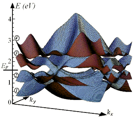
After diagonalization of the Hamiltonian (1) we arrive to the energy band spectrum where labels the energy bands of the electrons in the Bi/Si(111) system. The three-dimensional plot of the energy band structure is presented in Fig.2 for the four lowest bands labeled from 1 to 4. These lowest bands seem to be of the primary importance for the electron response analysis since the Fermi level is reportedly locatedFPG in the middle of them at eV, i.e. between the band No.2 and band No.3, as it can be seen in Fig.2. One of the most important features of the spectrum in Fig.2 stemming from the lattice geometry is the hexagonal symmetry of the energy bands in -space which implies, among other things, the absence of the symmetry, leading to rich properties of the spin response phenomena as we shall see below. It should be mentioned that the cross-sections of our 3D band plot shown here accurately repeat the 2D plots for the energy dispersion lines along various directions in the SBZ which were studied earlier in the framework of the NFE model.FPG We would like to add here just some new quantitative data: the cross-sections of the energy band surfaces along the direction reported previouslyFPG might created an impression of a large energy gap in the whole spectrum between bands 2 and 3 while the complete 3D presentation of these bands in Fig.2 indicates that the global structure of the energy bands in the whole 2D SBZ leaves this gap opened but with a much smaller width of around eV. Of course, the precise values of energy gaps may vary from model to model and can be specified more precisely during the future experimental and theoretical analysis.
Another important characteristic of quantum states in a system with significant SO coupling is the spin polarization of the eigenstates in the Brillouin zone which can be defined as the vector field in the reciprocal space with the components ()
| (6) |
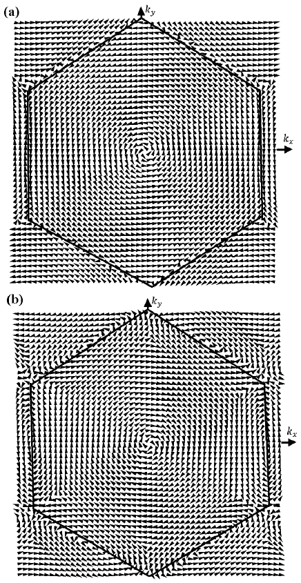
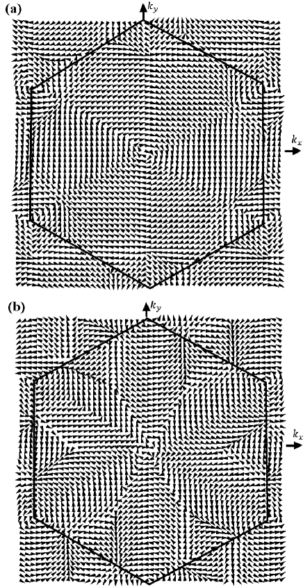
As usual for the Hamiltonian with a pure Rashba SO coupling term, the out-of-plane component of the spin field vanishes. The remaining components form a 2D spin polarization distribution in the SBZ which forms a specific vector field picture for each of the energy bands. In Fig.3 and Fig.4 we show the 2D spin polarization distributions for the lowest energy bands No.1 (Fig.3a), No.2 (Fig.3b), No.3 (Fig.4a) and No.4 (Fig.4b) from the band spectrum shown in Fig.2, with the hexagonal SBZ marked by a solid contour. As for the spins in two lowest subbands shown in Fig.3, one can see here that the initial Rashba counter clock-wise and clock-wise patterns of spin directions are present in a rather wide area surrounding the SBZ center, but more complicated vector field structure arises near the SBZ edge. The spin polarization in higher band No.3 and especially in band No.4 shown in Fig.4 demonstrates more new properties compared to the free Rashba states, including both the shape of the spin vector field which captures now more features of the hexagonal geometry of the SBZ, and the arising of new local vortices at various points of symmetry of the SBZ, mainly near its corners.
It can be concluded from the analysis of the spin polarization in the energy bands of Bi/Si system that certain properties of the initial basis of Rashba states remain visible. However, the change of the space symmetry to the hexagonal type without the element of axial symmetry and without the symmetry may probably lead to both common and distinct features in the current and spin response to the application of various external fields compared to the well-known properties of 2DEG with Rashba SO coupling. This assumption will be confirmed and illustrated below.
III Charge current and spin polarization response for dc field
It is known that the response of a two-dimensional electron gas with SO coupling to a constant electric field may be accompanied not only by the charge current but also by the spin polarization. Kleinert2005 ; Raichev2007 ; spinelec The most significant properties of such response for a pure Rashba SO term (3) in the Hamiltonian is the arising of the in-plane transverse polarization, i.e. the spin component when the electric field is applied along the direction while the out-of-plane component is absent in case of the accurately included relaxation processes which is sometimes related also to the absence of the spin Hall effect for a -linear Rashba model in the presence of the disorder.Inoue2004 So, it is natural to start the analysis of the electron system response with the calculation of the charge current and field-induced spin.
We shall start with the calculation of the non-equilibrium electric field-affected distribution function in the m-th energy band. If the system is subjected to a constant and uniform electric field parallel to the i-th axis, then in the collision frequency approximation the kinetic equation for can be written as spinelec
| (7) |
where is the collision rate and is the Fermi equilibrium distribution function in the -th band. Since the Bi/Si energy spectrum is characterized by a very large SO splitting and the band widths of the order of 1 eV, it may be a promising candidate for spin-dependent phenomena visible at room temperature. Thus, in the following we shall assume that K and consider a value of . As we have said before, the estimate for the collision rate as well for many other material parameters for the Bi/Si system is presently based on the assumptions rather than of the solid experimental facts since we are still in the beginning of the investigation for this new material. Still, we believe that our qualitative and sometimes quantitative results can be useful for predicting some novel properties of the electron and spin system response.
The mean charge current density measured for 2D system in units of current divided by the unit of transverse system size and the mean spin polarization , , can be found as spinelec
| (8) |
| (9) |
where is the surface concentration of the electrons on the Bi-covered Si surface, () are the Pauli matrices, and the velocity operator includes the SO part proportional to the Rashba parameter and acts on the spinor wavefunctions (2) via the matrices
| (10) |
| (11) |
In order to take a closer look for onto the expectations of the charge current density, we shall calculate and as well as and () by applying Eq.(8) for the electron surface concentration which may be reasonable since the surface density of atoms on Bi-covered Si(111) surface is estimated on the order of according to the experimental observations.Hirahara2007 ; Hirahara2007b
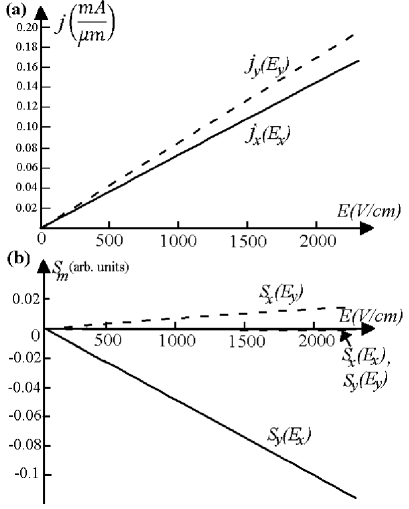
The results for the charge current density (8) and spin polarization (9) are shown in Fig.5(a) and Fig.5(b) respectively. One may see a conventional linear dependence of the charge current on the applied electric field throughout the whole range of fields up to kV/cm, and almost linear dependence for the significant non-zero induced spin components and . Other in-plane components and marked by arrow are also present in Fig.5 but their magnitude is much lower compared to and , and the out-of plane component is negligibly small. It is evident that the lattice asymmetry with respect to the interchange transform has lead to a slight but distinct asymmetry in the current amplitude of around , and the dominating and induced spin components demonstrate the well-known transverse in-plane character of the induced spin for linear Rashba SO coupling. It should be noted that the local probe measurements of induced spin polarizations (or magnetization) may detect the non-zero static and dynamic local magnetization Neudert2005 in the spot under the probe even in case of total zero mean spin value (9). The examples of such systems with zero total spin polarization but non-zero spin spatial distribution (spin textures) can be found among the models of semiconductor superlattices with SO coupling both withPSK and without sooptic ; spinelec external magnetic field, but their experimental observation and device application are currently limited by the probe and manipulation technology of the size of artificial superlattices and quantum wells rather then probing and utilizing the spatial magnetic configurations on the scale of individual atoms in the lattice. As to the predicted non-zero mean values of the induced spin such as those predicted here for Bi/Si, they are related to the whole sample and thus should be detectable. We believe that the predictions of the charge current and spin polarization generation made in this Sec. can be useful in designing novel spintronic devices where the induced spin components are coupled in a well-defined manner to the direction of the applied electric field, and this effect survives at room temperature and finite collision rate.
IV Spin polarization excited by electromagnetic field
The response of the spin system in materials with significant SO coupling on the application of an external electromagnetic radiation is among the most important and straightforwardly obtained characteristics since the optical manipulation of spins is one of the main goals of spintronics in general, and the linear response theory for the electromagnetic radiation effects is well-established and easily applied. It was found in various papers that the spins with different polarizations can be excited, depending on the symmetry of the electron Hamiltonian, the type and strength of the SO terms, and on the polarization of the incident radiation.Awschalom ; Zutic ; Bhat2005 ; Sherman2005 ; Tarasenko2005 ; Ganichev2007 ; sooptic ; PSK As in the previous Sec., we shall calculate the response functions for the room temperature and for a realistic collision broadening since the relatively large scale of energy bands and SO splitting in the Bi/Si electron system compared to the conventional GaAs, InGaAs or pure Si semiconductor structures can make Bi/Si being a promising candidate for the observation and control of the predicted radiation-induced effects in the devices operating even at room temperatures, as we hope.
The electromagnetic wave is considered to be propagating normally to the Bi/Si(111) interface along the axis, and is characterized by the polarization of the electric field vector in the plane, . In the dipole approximation the interaction of the electromagnetic field with the electrons is described via the velocity operators (10),(10) which include the SO part. We start with the calculation of the absorption coefficient
| (12) | |||
| (13) |
where is the polarization vector for the incident wave, is given by the velocity operators (10),(11), and are Fermi equilibrium distribution functions, is the sample volume, and the summation is taken over all energy bands , and the SBZ points . As we have already said, we don’t know yet the exact values for many of the material parameters for Bi/Si including the dielectric constant , and thus we shall focus mainly on the dependence of (13) on the incident wave frequency and will scale the absolute value of absorption in arbitrary units which can always be rescaled when the values material parameters will be clarified in future experiments.
The second quantity which frequency dependence we shall present together with the absorption is the induced spin polarization which can be derived by applying the Kubo linear response theoryKubo1957 ; Callaway1974 ; PSK and has the following form:
| (14) | |||
| (15) |
Here the interband matrix elements of the spin -th component operator as well as the matrix elements for the -th component of the velocity operator (10),(11) enter depending on the incident wave polarization and on the desirable output for the spin component, , the parameter is level broadening which we take as being equal to the collision rate introduced in the previous Sec, and is the unit cell volume. As before, we shall assume that K and which should provide us with realistic expectations regarding the absorption and induced spin dependence on the incoming photon energy.
The results for the photon energy dependence of the absorption coefficient (13) and the induced spin polarization (15) are shown in Fig.6 through Fig.9 for the incident wave linearly polarized along (Fig.6), along (Fig.7) directions, and for circular (Fig.8) and (Fig.9) polarizations. The photon energy interval is chosen to cover the whole energy band range of the four lowest bands shown in Fig.2 where the most effective transitions occur between the states below and above the Fermi level. One can see that both the in-plane spin components , and the out-of plane component can be excited on a comparable scale which is a distinguishable feature of the lower hexagonal symmetry combined with Rashba SO coupling compared with one-dimensionalKleinert2005 ; sooptic ; spinelec or two-dimensional squarePSK lattices with Rashba SO coupling.
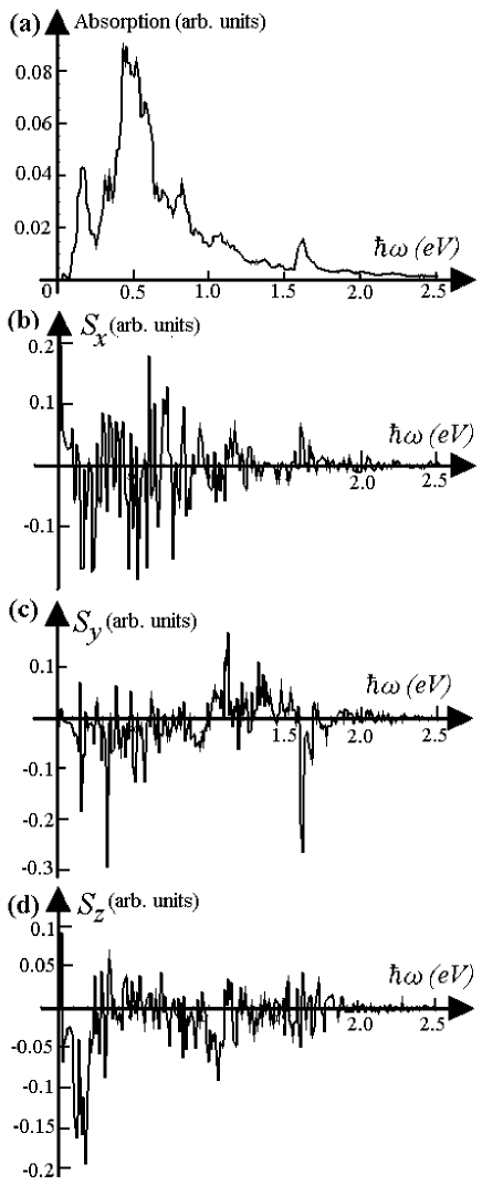
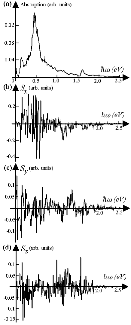
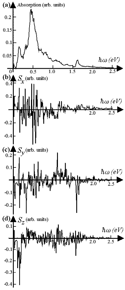
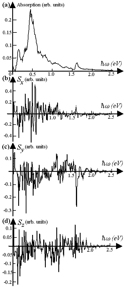
If one compares the results for - and -polarized radiation in Fig.6 and Fig.7, it can be seen that, similar to the dc current properties discussed in the previous Sec., the lattice and energy band asymmetry in the hexagonal geometry of the whole problem is reflected here in different shape and amplitude for the absorption coefficients in Fig.6(a) and 7(a). Again, by looking onto the relative magnitude of the excited spin components in Fig.6(b)-(d) and in Fig.7(b)-(d) one can see that the pure Rashba SO coupling is reflected in the dominating excited component in Fig.6 and correspondingly in the dominating component in Fig.6, i.e., in the in-plane and transverse direction relative to the electric field vector of the incident wave. As to the results for the circular -polarized radiation presented in Fig.8 and Fig.9, on can see that the common features of the response to both -polarized and -polarized incoming wave from Fig.6 and Fig.7 can be seen on the spin component figures since both and operators here enter the expressions (13) and (15) for the response. The absorption coefficient is totally insensible to the direction of rotation for the incoming wave as it can be seen by comparing Fig.8(a) and Fig.9(a). The shape of the photon energy dependence for the excited spin components in Fig.8(b)-(d) and Fig.9(b)-(d) is different for and polarizations, but these differences have a quantitative rather than a qualitative character since the hexagonal symmetry of the lattice and the energy bands does not make any of these two polarizations preferable from the point of view of the response quantities (13) and (15).
In conclusion, the calculation and analysis of the absorption and spin polarization response to the monochromatic electromagnetic radiation with normal incidence and having different polarizations demonstrates that this radiation is most effectively absorbed in the photon energy range of around eV corresponding to the photon wavelength where both in-plane and out-of-plane spin components can be excited at realistic temperature and collision broadening on a comparable scale with relative amplitudes depending on the precise value of frequency and the polarization of the incident radiation. These properties can be useful for designing new optical and spintronic devices coupling the electron spin with light and operating at room temperature.
V Conclusions
We have developed an expansion of the nearly free-electron modelFPG describing the energy bands and spin polarization for the electron states at Bi/Si(111) interface with giant spin-orbit coupling, and applied it for the linear response analysis for charge current and induced spin caused by dc field and by electromagnetic radiation. It was found that the large spin-orbit coupling in this system may allow resolving the spin-dependent properties even at room temperature and at realistic collision rate. The geometry of the atomic lattice combined with spin-orbit coupling leads to an anisotropic response both for current and spin components related to the orientation of the external field. The in-plane dc electric field produces only the in-plane components of spin in the sample while both the in-plane and out-of-plane spin components can be excited by normally propagating electromagnetic wave with different polarizations. The qualitative predictions of the charge and spin response in a novel and promising Bi/Si system may be useful for the forthcoming detailed theoretical and experimental studies which may lead to the development of principally new electronic, optical and spintronic devices operating at room temperature. Further theoretical and especially experimental studies of this promising system with big SO coupling allowing the survivability of the spin-related effects at room temperature are expected bringing us new and fascinating phenomena with both fundamental, experimental and device-related results.
Acknowledgments
The author is grateful to V.Ya. Demikhovskii, A.M. Satanin, A.A. Perov for helpful discussions, and to A.A. Chubanov for technical assistance. The work was supported by the RFBR Grants 11-02-00960a and 11-02-97039/Regional, and by the RNP Program of Ministry of Education and Science RF.
References
- (1) E. Frantzeskakis, S. Pons, and M. Grioni, Phys. Rev. B 82, 085440 (2010).
- (2) Semiconductor Spintronics and Quantum Computation, edited by D.D. Awschalom, D. Loss, and N. Samarth, Nanoscience and Technology (Springer, Berlin, 2002).
- (3) I. Zǔtić, J. Fabian, and S. Das Sarma, Rev. Mod. Phys. 76, 323 (2004).
- (4) M.W. Wu, J.H. Jiang, and M.Q. Weng, Phys. Rep. 493, 61 (2010).
- (5) R. Shioda, A. Kawazu, A.A. Baski, C.F. Quate, and J. Nogami, Phys. Rev. B 48, 4895 (1993).
- (6) R.H. Miwa and G.P. Srivastava, Phys. Rev. B 66, 235317 (2002).
- (7) R.H. Miwa, T.M. Schmidt, and G.P. Srivastava, J. Phys. C 15, 2441 (2003).
- (8) T. Hirahara, T. Nagao, I. Matsuda, G. Bihlmayer, E.V. Chulkov, Yu.M. Koroteev, P.M. Echenique, M. Saito, and S. Hasegawa, Phys. Rev. Lett. 97, 146803 (2006).
- (9) T. Hirahara, T. Nagao, I. Matsuda, G. Bihlmayer, E.V. Chulkov, Yu.M. Koroteev, and S. Hasegawa, Phys. Rev. B 75, 035422 (2007).
- (10) T. Hirahara, K. Miyamoto, I. Matsuda, T. Kadono, A. Kimura, T. Nagao, G. Bihlmayer, E.V. Chulkov, S. Qiao, K. Shimada, H. Namatame, M. Taniguchi, and S. Hasegawa, Phys. Rev. B 76, 153305 (2007).
- (11) E. Frantzeskakis, S. Pons, H. Mirhosseini, J. Henk, C.R. Ast, and M. Grioni, Phys. Rev. Lett. 101, 196805 (2008).
- (12) J.H. Dil, F. Meier, J. Lobo-Checa, L. Patthey, G. Bihlmayer, and J. Osterwalder, Phys. Rev. Lett. 101, 266802 (2008).
- (13) I. Gierz, T. Suzuki, E. Frantzeskakis, S. Pons,, S. Ostanin, A. Ernst, J. Henk, M. Grioni, K. Kern, and C.R. Ast, Phys. Rev. Lett. 103, 046803 (2009).
- (14) G. Bian, T. Miller, and T.-C. Chiang, Phys. Rev. B 80, 245407 (2009).
- (15) K. Sakamoto, H. Kakuta, K. Sugawara, K. Miyamoto, A. Kimura, T. Kuzumaki, N. Ueno, E. Annese, J. Fujii, A. Kodama, T. Shishidou, H. Namatame, M. Taniguchi, T. Sato, T. Takahashi, and T. Oguchi, Phys. Rev. Lett. 103, 156801 (2009).
- (16) G. Jnawali, H. Hattab, B. Krenzer, and M. Horn von Hoegen, Phys. Rev. B 74, 195340 (2006).
- (17) G. Jnawali, H. Hattab, F.J. Meyer zu Heringdorf, B. Krenzer, and M. Horn-von Hoegen, Phys. Rev. B 76, 035337 (2007).
- (18) R.H. Miwa, T.M. Schmidt, and P. Venezuela, Phys. Rev. B 72, 125403 (2005).
- (19) J. Mysliveček, F. Dvořák, A. Stróżecka, and B. Voigtländer, Phys. Rev. B 81, 245427 (2010).
- (20) R.H. Miwa and G.P. Srivastava, Phys. Rev. B 74, 035301 (2006).
- (21) R.H. Miwa, W. Orellana, and G.P. Srivastava, Phys. Rev. B 78, 115310 (2008).
- (22) A. Hanisch, B. Krenzer, T. Pelka, S. Möllenbeck, and M. Horn-von Hoegen, Phys. Rev. B 77, 125410 (2008).
- (23) M.S. Bahramy, R. Arita, and N. Nagaosa, arXiv:1105.2757 (2011).
- (24) V.M. Edelstein, Solid State Commun. 73, 233 (1990).
- (25) A.G. Aronov, Yu.B. Lyanda-Geller, and G.E. Pikus, Zh. Eksp. Teor. Fiz. 100, 973 (1991) [Sov. Phys. JETP 73, 537 (1991)].
- (26) P. Kleinert, V.V. Bryksin, O. Bleibaum, Phys. Rev. B 72, 195311 (2005).
- (27) O.E. Raichev, Phys. Rev. B 75, 205340 (2007).
- (28) R.D.R. Bhat, F. Nastos, Ali Najmaie, and J.E. Sipe, Phys. Rev. Lett. 94, 096603 (2005).
- (29) A. Najmaie, E.Ya. Sherman, and J.E. Sipe, Phys. Rev. Lett. 95, 056601 (2005).
- (30) S.A. Tarasenko, Phys. Rev. B 72, 113302 (2005).
- (31) S. Giglberger, L.E. Golub, V.V. Bel’kov, S.N. Danilov, D. Schuh, C. Gerl, F. Rohlfing, J. Stahl, W. Wegscheider, D. Weiss, W. Prettl, and S.D. Ganichev, Phys. Rev. B 75, 035327 (2007).
- (32) Z.-G. Zhu, C.-L. Jia, and J. Berakdar, Phys. Rev. B 82, 235304 (2010).
- (33) V.Ya. Demikhovskii and D.V. Khomitsky, JETP Letters 83, 340 (2006) [Pis’ma v ZhETF 83, 399 (2006)].
- (34) D.V. Khomitsky, Phys. Rev. B 77, 113313 (2008).
- (35) A.A. Perov, L.V. Solnyshkova, and D.V. Khomitsky, Phys. Rev. B 82, 165328 (2010).
- (36) D.V. Khomitsky, Phys. Rev. B 79, 205401 (2009).
- (37) Y.V. Pershin, Phys. Rev. B 71, 155317 (2005).
- (38) P. Stano and J. Fabian, Phys. Rev. B 74, 045320 (2006).
- (39) J.I. Inoue, G.E.W. Bauer, and L.W. Molenkamp, Phys. Rev. B 70, 041303(R) (2004).
- (40) A. Neudert, J. McCord, D. Chumakov, R. Schäfer, and L. Schultz, Phys. Rev. B 71, 134405 (2005).
- (41) R. Kubo, J. Phys. Soc. Jpn. 12, 570 (1957).
- (42) C.S. Wang and J. Callaway, Phys. Rev. B 9, 4897 (1974).