Ordered Semiconducting Nitrogen-Graphene Alloys
Abstract
The interaction between substitutional nitrogen atoms in graphene is studied by performing first principles calculations. The nearest neighbor interaction between nitrogen dopants is highly repulsive because of the strong electrostatic repulsion between nitrogen atoms, which prevents the full phase separation in nitrogen doped graphene. Interestingly, there are two relatively stable nitrogen-nitrogen pairs due to the anisotropy charge redistribution induced by nitrogen doping. We reveal two stable semiconducting ordered N doped graphene structures C3N and C12N through the cluster expansion technique and particle swarm optimization method. In particular, C12N has a direct band gap of 0.98 eV. The heterojunctions between C12N and graphene nanoribbons might be promising organic solar cells.
pacs:
61.48.Gh,73.61.Wp,71.20.-b,73.22.-fIntroduction
Graphene, a single layer of carbon atoms arranged in a honeycomb lattice, has been the focus of recent research efforts Novoselov2005 ; Novoselov2006 ; Zhang2005 , due to its unique zero-gap electronic structure and the massless Dirac fermion behavior. The unusual electronic and structural properties make graphene a promising material for the next generation of faster and smaller electronic devices. However, graphene lacks an essential feature for controlled and reliable transistor operation, namely, a band gap around the Fermi level. Several schemes have been proposed to open a band gap in graphene. One is the substrate-induced gap for graphene supported on SiC Zhou2007 , but the experimental realization of this idea turned out to be very difficult and controversial Rotenberg2008 . Another approach is the creation of gaps through confinement Yang2007 , such as in narrow graphene nanoribbons (GNRs). However, a large scale production of narrow GNRs is still very challenging. In addition, it was demonstrated that the band gap of a graphene bilayer can be controlled externally by applying a gate bias Zhang2009 ; Castro2007 . Unfortunately, bandgap tailoring by external electrostatic gate has limited tunability for the transistor on-off ratio. Chemical functionalization Bekyarova2009 ; Sarkar2011 is an alternative way to manipulate the electronic properties of graphene. The hydrogenation of graphene Sofo2007 ; Bekyarova2009 ; Ryu2008 ; Boukhvalov2009 ; Xiang2009 ; Xiang2010b ; Lu2009 ; Zhou2009 , as a prototype of covalent chemical functionalization, was studied extensively. However, the fully hydrogenated graphene, i.e., graphane CH, is an insulator with a very large band gap (larger than 5 eV) Lebegue2009 , which prevents from using graphane in a field-effect transistor. There were some efforts to tune the band gap of two-dimensional (2D) graphene by varying the hydrogen concentration. Unfortunately, the phase separation between bare graphene and graphane will take place spontaneously, leading to an essential zero band gap for the whole system Xiang2009 . Similar phenomenon was found to also occur in the oxidized graphene Xiang2010 .
Previous studies Yu2010 ; Li2009 ; Biel2009 ; Lherbier2008 ; Huang2011 ; Wang2009 revealed that doping graphene and related materials with nitrogen is effective to tailor its electronic property and chemical reactivity because of the stronger electronegativity of nitrogen compared to that of carbon and conjugation between the nitrogen lone pair electrons and the graphene -system. This could create novel nanomaterials and expand its already widely explored potential applications. Experiments Deng2011 suggest that nitrogen species have been incorporated into the graphene structure with content in the range of 4.5-16.4%. Usually, the nitrogen atoms are substitutionally incorporated into the basal plane of graphene in the forms of pyridinic, pyrolic and graphitic nitrogen bonding configurations. X-ray photoelectron spectroscopy showed that the pyridinic and pyrolic nitrogen may lie at the edge or the defect sites and the graphitic nitrogen (the nitrogen replacing carbon in graphene plane) is dominant Liu2011 . A recent scanning tunneling microscopy study also showed that individual nitrogen atoms were incorporated as graphitic dopants Zhao2011 . Theoretically, the isolated substitutional nitrogen doping in graphene was studied before Zhao2011 . However, the nature of the interaction between substitutional nitrogen atoms is far from clear. How the electronic structures of graphene is modified by multiple nitrogen dopants is an interesting open question to be addressed.
In this paper, we examine the collective behavior of nitrogen doping in graphene on the basis of density functional calculations. We find that the nearest neighbor interaction between nitrogen dopants is highly repulsive because of the strong electrostatic repulsion between negatively charged nitrogen atoms. Our calculations reveal two stable ordered N doped graphene structures C3N and C12N. Surprisingly, nitrogen atoms do not simply doping electrons to the graphene state. Instead, both ordered structures are found to be semiconducting. In particular, C12N has a direct band gap of 0.98 eV. The substitutional nitrogen raises the valence band maximum (VBM) and conduction band minimum (CBM) level in N doped graphene, leading to a type-II band alignment between C12N and 6-AGNR. We propose that C12N/6-AGNR is a promising organic solar cell with C12N as donor and 6-AGNR as acceptor, respectively.
Computational Method
In our DFT calculations, the local density approximation (LDA) was adopted unless otherwise stated. The plane-wave cutoff energy for wavefunction was set to 500 eV. The ion-electron interaction was treated using the projector augmented wave (PAW) PAW technique as implemented in the Vienna ab initio simulation package VASP . For the Brillouin zone sampling, we use Monkhorst-Pack k-mesh for the graphene supercell. And for C3N (C12N), we used the ( ) Monkhorst-Pack k-mesh. The constant temperature first-principles molecular dynamics simulations were performed to check the thermal stability of C3N and C12N. The “cluster expansion” Ferreira1989 of the alloy Hamiltonian was carried out by the ATAT package atat . The global minimum optimization was performed using the two-dimensional (2D) particle swarm optimization (PSO) technique, which we proposed recently to predict the most stable 2D crystals Luo2011 . For the PSO simulations, we use the Crystal structure AnaLYsis by Particle Swarm Optimization (CALYPSO) code Wang2010 .
Results and Discussion
Interaction Between Nitrogen Dopants
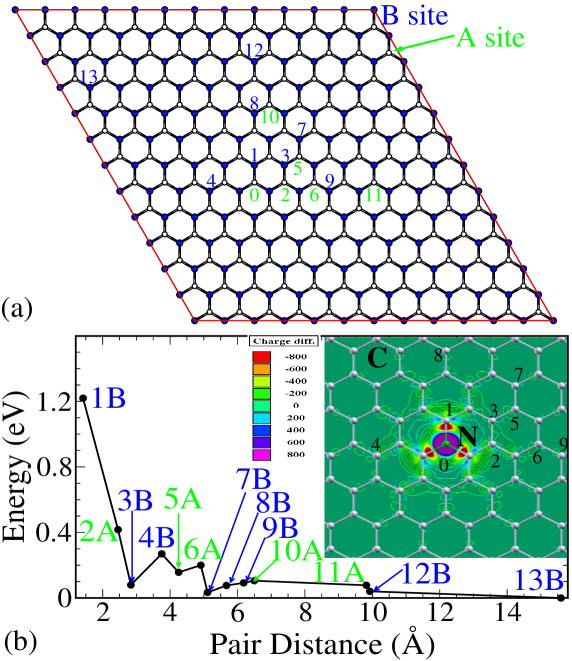
To investigate the interaction between two substitutional nitrogen atoms, we use a supercell of graphene. The use of such a large supercell is essential due to the relative long range interaction between nitrogen dopants. And test calculation shows that using larger supercells gives similar results. As is well known, the honeycomb lattice of graphene consists of two interpenetrating triangular sublattices, namely sublattice A and sublattice B. We consider the interaction between a nitrogen atom at 0A site and those at other sites [see Fig. 1(a)]: All interaction with the interaction range less than 6.5 Å are included, and we also include several other longer range interaction N-N pairs (0A-11A, 0A-12B, 0A-13B). For each N-N pair, the internal atomic structure is fully relaxed. With respect to the energy of longest N-N pairs 0A-13B considered in this work (15.60 Å), We plot the interaction energy of other N-N pairs in Fig. 1(b). First, we can see that all the interaction energy are positive, i.e., the interactions are repulsive. This can be understood because nitrogen has a high electronegativity than carbon thus nitrogen atoms are surrounded by more electrons which leads to the repulsive electrostatic interaction. Second, the nearest neighbor interaction is extremely repulsive. This is because the two nitrogen atoms are directly connected along the bond direction leading to a very strong electrostatic repulsion. Third, generally the interaction energy decreases with the pair distance because of the nature of coulombic electrostatic interaction. Fourth, for N-N pairs with short pair distances (less than 6.5 Å), the interaction energy curve has two local minima at N-N pairs 0A-3B and 0A-7B. The interaction between 0A and 3B and that between 0A and 7B are only slightly repulsive with the interaction energies of 0.08 eV and 0.03 eV, respectively.
The nontrivial non-monotonic dependence of the pair interaction energy on the N-N distance and the presence of local minima at N-N pairs 0A-3B and 0A-7B are interesting findings to be understood. Our calculations show that the strain relaxation is not responsible for the stability of the 0A-3B and 0A-7B N-N pairs because the energies of the unrelaxed pair structures display the same trend. Instead, we find that the stability of the 0A-3B and 0A-7B N-N pairs is due to the anisotropic electron charge density redistribution induced by the nitrogen substitution. Fig. 1(b) shows the charge difference between the isolated N-doped graphene and the undoped graphene. We can see that the charge redistribution in graphene is mainly along the nearest neighbor bonding direction. Since sites 3B and 7B are nearly opposite to the bonding direction, there is much less charge redistribution around site 3B (7B) than that around 2A and 4B (6A and 8B). Therefore, in the case of the 0A-3B and 0A-7B N-N pairs, the coulombic repulsion will be weaker than that between the other neighboring pairs.
Our calculations show that the interaction between substitutional nitrogen atoms in graphene differs fundamentally from that between adsorbed hydrogen (oxygen) atoms on graphene. In the hydrogenated (oxidized) graphene case, hydrogen (oxygen) tends to be close to each other in order to lower the kenetic energy of the carbon electrons, leading to the phase separation between fully hydrogenated (oxidized) graphene and bare grapheneXiang2009 ; Xiang2010 . The repulsive interaction between substitutional nitrogen atoms will prevent the phase separation of nitrogen doped graphene into undoped graphene part and highly nitrogen doped graphene part, in contrast to the case of the hydrogenation and oxidization of graphene Xiang2009 ; Xiang2010 .
Ordered Semiconducting Nitrogen-Graphene Alloys
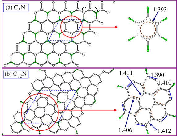
In our above discussions, 0A-3B and 0A-7B are two relatively stable configurations of N-N pairs. For each type of two pairs, we can construct a graphene superstructure with a uniform distribution of nitrogen dopants. For the 0A-3B N-N pair, the ordered nitrogen doped graphene structure is a superstructure (C3N) of the graphene, as shown in Fig. 2(a). We can see that the doped nitrogen atoms themselves form a honeycomb lattice, similar to graphene but with a doubled lattice constant. As a consequence, the carbon atoms are separated into isolated six-membered rings, as shown in the right panel of Fig. 2(a). For the 0A-7B N-N pair, the ordered nitrogen doped graphene structure is a -R46.1∘ superstructure (C12N) of the graphene, as shown in Fig. 2(b). In this superstructure, the carbon atoms are connected by carbon-carbon bonds to form a single carbon domain, in contrast to the C3N case.
To examine the stability of the C3N and C12N superstructures, we use “cluster expansion” method Ferreira1989 and direct comparison of total energies between different superstructures. In the “cluster expansion” method, the alloy Hamiltonian is mapped onto a generalized Ising Hamiltonian. In brief, for some nitrogen doped graphene configurations, we perform spin polarized DFT calculations to relax the cell and internal atomic coordinates. The energies of the relaxed structures are used to extract the interaction parameters of the alloy Hamiltonian. After obtaining the interaction parameters (See Supplemental Material support ) of the alloy Hamiltonian, we find that the C3N superstructure shown in Fig. 2(a) is the most stable structure for the CxN alloy with the 25% nitrogen concentration (at least for cells with no more than 32 atoms). For the C12N superstructure with the 0A-7B N-N pairs, the relatively long range (5.11 Å) pair interaction is not included in the alloy Hamiltonian. Therefore, we generate all superstructures with no more than 26 atoms and the same nitrogen concentration (7.7%) as C12N using the linear scaling algorithm recently proposed by Hart and ForcadeHart2009 . Our calculations show that the C12N superstructure shown in Fig. 2(b) has the lowest energy among all considered structures. The lattice dynamics calculation shows that both C3N and C12N have no imaginary frequency phonon and thus are stable support . First-principles molecular dynamic simulations up to 500 K were performed to check the stability of C3N and C12N. We find that the N atoms only vibrate around the equilibrium position, which confirms the thermal stability of C3N and C12N.
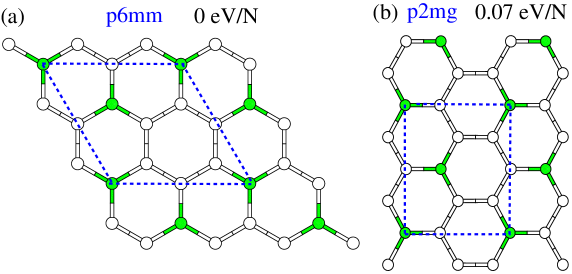
Above we proposed two possible stable ordered nitrogen-carbon alloys (C3N and C12N shown in Fig. 2) by considering only the graphene-based structures. Here, we perform PSO global minimum optimization to confirm the proposed structures. In the 2D PSO simulations Luo2011 , the graphene lattice structure is not assumed. Instead, we generate random structures (both atomic positions and cell parameters) to initialize the simulations. The initial structures are subsequently relaxed before performing the PSO operations. The population size is set to 30. We consider all possible cell sizes with the total number of atoms no more than 26. The number of generations is fixed to 30. Our simulations show that the most stable 2D nitrogen-carbon alloy structure with 25% N concentration is indeed the structure ( plane group) shown in Fig. 2(a) [see also Fig. 3(a)]. The second lowest energy 2D structure with the plane group [Fig. 3(b)] has a higher energy by 0.07 eV/N. It should be noted that both and structures can be viewed as nitrogen doped graphene structures although the graphene honeycomb lattice is not assumed in the PSO simulations. The PSO simulations for the 2D nitrogen-carbon alloy structure with 7.7% nitrogen concentration do not give structures more stable than the C12N shown in Fig. 2(b), in support of the stability of the proposed C12N structure. We note that the formation energies of C3N and C12N are positive if graphene and N2 molecule are taken as the references. However, many experiments Wang2009 ; Zhao2011 showed that N atoms can be incorporated into graphene. Here we show that C3N and C12N are the most stable structures once N atoms are incorporated into graphene, as can be seen from the convex hull plot in the new supporting material support .
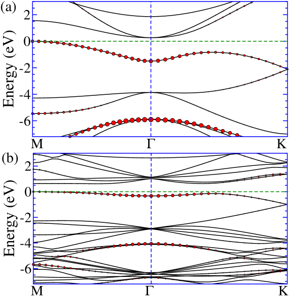
The band structures for the C3N and C12N superstructures from the LDA calculations are shown in Fig. 4(a) and (b), respectively. Interestingly, both superstructures are found to be semiconductors: C3N has an indirect band gap (about 0.26 eV from the LDA calculation) with the VBM at and CBM at , respectively; C12N has instead a direct band gap (about 0.62 eV from the LDA calculation) at the point. Because the orbital of a nitrogen atom will be almost fully occupied by the two electrons, the mechanism for the band gap opening in graphene induced by nitrogen doping can be understood by examining only the bonding situation of carbon electrons. Recently, Clar’s theory of the aromatic sextet Clar1972 was shown to be a simple and powerful tool to predict the stability and the electronic/magnetic structure of graphene related systems. According to Clar’s rule, for a given system, the representation with a maximum number of Clar sextets, called the Clar formula, is the most representative one. Here, we show the Clar formulas for C3N and C12N in the right panels of Figs. 2(a) and (b), respectively. In C3N, each six-membered ring forms a Clar sextet. And C3N has one unique Clar formula, thus belongs to the class 1CF of the (pseudo)-all-benzenoid structure. In contrast, C12N has no Clar sextets, and thus are nonbenzenoid. Because each nitrogen atom forms three single bonds with the neighboring carbon atoms, the nitrogen atoms are excluded when constructing the Clar formula. We note that in the Clar formula for the -NH terminated graphene nanoribbon, the two N-C bonds were also treated as single bonds Seitsonen2010 . The Clar formulas shown in Figs. 2 are in good agreement with the C-C bond lengths of relaxed structures from the DFT calculation. All the C-C bond lengths in C3N are the same, i.e., 1.393 Å. For C12N, some C-C bonds (marked by an additional solid line) have short bond lengths, 1.388 Å, which can be considered as normal C-C double bond; and there are weak C-C double bonds (marked by an additional dashed line) with the bond lengths of 1.406 Å; all the other C-C bonds are single bond. Wassmann et al. Wassmann2010 showed that all graphene related structures has a relative large band gap except for the (pseudo)-all-benzenoid structure with class nCF () such as graphene which has small or zero band gap. Therefore, we expect that there is a large band gap between the occupied carbon states and the unoccupied carbon states in both C3N and C12N. Our analysis for the wavefunction characters indicates that the highest occupied band near is mainly contributed by nitrogen orbitals and there are some contributions from carbon orbitals when approaching the Brillouin zone boundary. The lowest unoccupied band is mostly contributed by the carbon orbitals. The gap between the highest occupied carbon state and the CBM is larger than 1.5 eV (in LDA) in both C3N and C12N, which is in accord with the Clar’s theory. The small band gaps for C3N and C12N are due to the presence of the nitrogen state (VBM state) above the highest occupied carbon state. C3N has a smaller band gap because the direct hopping between N orbitals in C3N leads to the larger dispersion of the highest occupied band. We note that the dilute limit of nitrogen substitutional doping in graphene was experimentally studied by Zhao et al. Zhao2011 , where the extra electron of the nitrogen dopant was found to delocalized into the neighboring graphene lattice, resulting in the n-type behavior. In this work, we predict that collective nitrogen doping can induce exotic semiconducting behavior in graphene. Experimentally, some disorder in the nitrogen distribution might occur due to the thermal fluctuation. To see the effect of the disorder on the band gap, we have simulated a disordered configuration with 12.5% N concentration using a 128-atom special quasirandom structure SQS . The LDA band gap is found to be 0.08 eV. The real band gap should be larger because the LDA functional underestimates the band gap. This suggests that the disorder might change the magnitude the band gap, but shall not close it. Moreover, because the ordered C3N and C12N is more stable at low temperature than the disordered one, we believe reasonably large band gap should exist in nitrogen doped graphene synthesized at low temperature.
It is well-known that LDA seriously underestimates the band gap of semiconductors, thus we calculate the electronic structures of C3N and C12N by employing the screened Heyd-Scuseria-Ernzerhof 06 (HSE06) hybrid functional Heyd2003 ; Krukau2006 ; Paier2006 , which was shown to give a good band gap for many semiconductors including graphene related systems Hod2008 . Our HSE06 calculations show that C3N and C12N have the band gaps of 0.96 eV and 0.98 eV, respectively. It is noted that the band gaps of the nitrogen doped graphene are close to the band gap (about 1.12 eV) in silicon. This suggests that C3N and C12N with similar electronic properties as silicon might be promising electronic materials for the next generation CMOS technology.
Potential Organic Solar Cell
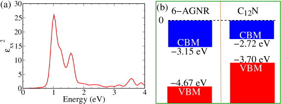
The fact that C12N has a direct band gap of 0.98 eV suggests that C12N might be a promising solar cell absorption material. To investigate this possibility, we calculate the imaginary part of the frequency dependent dielectric function via summation over pairs of occupied and empty states without considering the local field effects using the HSE06 screened hybrid function. Fig. 5(a) shows the calculated result () for one of the diagonal parts of the in-plane components. We can see that there is a very strong peak at around 1.0 eV arising from the interband HOMO-LUMO transition. Such strong adsorption peak is due to the fact that both the VBM band and CBM band around M are rather flat. Due to the dispersion of the VBM band and CBM band at other K-points, there is also substantial optical absorption up to 1.6 eV. The absorption between 1.9 eV and 4.0 eV is rather weak, indicating that a solar cell with only C12N might be not efficient because the solar energy between 1.9 eV and 4.0 eV may not be absorbed completely. Our HSE06 calculation shows that C12N has a relatively high VBM level ( eV with repect to the vacuum level). This suggests that C12N can act as a donor. If an appropriate acceptor material can be found, we can construct a photovoltaic system with a similar architecture as the P3HT/C60-PCBM bulk heterojunction solar cell. We find from HSE06 calculations that the the VBM and CBM levels of 6-AGNR are eV and eV, respectively. Therefore, the band alignment between C12N and 6-AGNR is of type-II, as shown in Fig. 5(b). In this proposed C12N/6-AGNR solar cell, C12N can absorb the solar energy between 0.98 eV and 1.50 eV. And 6-AGNR can absorb the solar energy above the band gap 1.52 eV. The eletron-hole pair excited by photo can be separated by the field due to the type-II band alignment.
Conclusion
In summary, we have studied the interaction between substitutional nitrogen atoms in graphene and find that the nearest neighbor interaction between nitrogen dopants is highly repulsive because of the strong electrostatic repulsion between nitrogen atoms. Our calculations reveal two stable ordered N doped graphene structures C3N and C12N. Both structures are semiconducting, in contrast to the common belief that nitrogen atoms simply dope electrons to the graphene Dirac cone. In particular, C12N has a direct band gap of 0.98 eV. The substitutional nitrogen raises the VBM and CBM level in N doped graphene, leading to a type-II band alignment between C12N and 6-AGNR. We propose that C12N/6-AGNR is a promising organic solar cell with C12N as donor and 6-AGNR as acceptor, respectively. Our study suggests that nitrogen doping might be a promising way to open a band gap in grapene for the application in electronics and photovoltaics.
Acknowledgment
Work at Fudan was partially supported by the National Science Foundation of China, Pujiang plan, and The Program for Professor of Special Appointment (Eastern Scholar) at Shanghai Institutions of Higher Learning. Work at NREL was supported by the LDRD program funded by the U.S. Department of Energy, under Contract No. DE-AC36-08GO28308.
References
- (1) K. S. Novoselov, A. K. Geim, S. V. Morozov, D. Jiang, M. I. Katsnelson, I. V. Grigorieva, S. V. Dubonos, and A. A. Firsov, Two-dimensional gas of massless Dirac fermions in graphene, Nature (London) 438, 197 (2005).
- (2) K. S. Novoselov, E. McCann, S. V. Morozov, V. I. Fal ko, M. I. Katsnelson, U. Zeitler, D. Jiang, F. Schedin, and A. K. Geim, Unconventional quantum Hall effect and Berry’s phase of 2 in bilayer graphene, Nat. Phys. 2, 177 (2006).
- (3) Y. Zhang, Y.-W. Tan, H. L. Stormer, and P. Kim, Experimental observation of the quantum Hall effect and Berry’s phase in graphene, Nature (London) 438, 201 (2005).
- (4) S. Y. Zhou, G.-H. Gweon, A. V. Fedorov, P. N. First, W. A. De Heer, D.-H. Lee, F. Guinea, A. H. Castro Neto, and A. Lanzara, Substrate-induced bandgap opening in epitaxial graphene, Nat. Mater. 6, 770 (2007); Franois Varchon, R. Feng, J. Hass, X. Li, Bich N. Nguyen, Ccile Naud, Pierre Mallet, Jean Yves Veuillen, Claire Berger, E. H. Conrad, and Laurence Magaud, Electronic structure of epitaxial graphene layers on SiC: Effect of the substrate, Phys. Rev. Lett. 99, 126805 (2007).
- (5) E. Rotenberg, A. Bostwick, T. Ohta, J. L. McChesney, T. Seyller, and K. Horn, Origin of the energy bandgap in epitaxial graphene, Nat. Mater. 7, 258 (2008); S. Y. Zhou, D. A. Siegel, A. V. Fedorov, F. E. Gabaly, A. K. Schmid, A. H. C. Neto, D. H. Lee, and A. Lanzara, Origin of the energy bandgap in epitaxial graphene-Reply, Nat.Mater. 7, 259 (2008).
- (6) L. Yang, C. H. Park, Y. W. Son, M. L. Cohen, and S. G. Louie, Quasiparticle energies and band gaps in graphene nanoribbons, Phys. Rev. Lett. 99, 186801 (2007).
- (7) Y. Zhang, T. T. Tang, C. Girit, Z. Hao, M. A. Martin, A. Zettl, M. F. Crommie, Y. R. Shen, and F. Wang, Direct observation of a widely tunable bandgap in bilayer graphene, Nature 459, 820 (2009).
- (8) E. V. Castro, K. S. Novoselov, S. V. Morozov, N. M. R. Peres, J. M. B. Lopes dos Santos, Johan Nilsson, F. Guinea, A. K. Geim, and A. H. Castro Neto, Biased bilayer graphene: Semiconductor with a gap tunable by the electric field effect, Phys. Rev. Lett. 99, 216802 (2007).
- (9) E. Bekyarova, M. E. Itkis, P. Ramesh, C. Berger, M. Sprinkle, W. A. de Heer, and R. C. Haddon, Chemical Modification of Epitaxial Graphene: Spontaneous Grafting of Aryl Groups, J. Am. Chem. Soc. 131, 1336 (2009).
- (10) S. Sarkar, E. Bekyarova, S. Niyogi, and R. C. Haddon, Diels-Alder Chemistry of Graphite and Graphene: Graphene as Diene and Dienophile, J. Am. Chem. Soc. 133, 3324 (2011).
- (11) S. Ryu, M. Y. Han, J. Maultzsch, T. F. Heiz, P. Kim, M. L. Steigerwald, and L. E. Brus, Reversible Basal Plane Hydrogenation of Graphene, Nano Lett. 8, 4597 (2008).
- (12) H. J. Xiang, E. J. Kan, S.-H. Wei, M.-H. Whangbo, and J. L. Yang, “Narrow” Graphene Nanoribbons Made Easier by Partial Hydrogenation, Nano Lett. 9, 4025 (2009).
- (13) H. J. Xiang, E. J. Kan, S.-H. Wei, X. G. Gong, and M.-H. Whangbo, Thermodynamically stable single-side hydrogenated graphene, Phys. Rev. B 82, 165425, (2010).
- (14) D. W. Boukhvalov and M. I. Katsnelson, Chemical functionalization of graphene, J. Phys.: Condens. Matter 21, 344205 (2009).
- (15) J. O. Sofo, A. S. Chaudhari, and G. D. Barber, Graphane: A two-dimensional hydrocarbon, Phys. Rev. B 75, 153401 (2007).
- (16) J. Zhou, Q. Wang, Q. Sun, X. S. Chen, Y. Kawazoe, and P. Jena, Ferromagnetism in Semihydrogenated Graphene Sheet, Nano Lett. 9, 3867 (2009).
- (17) N. Lu, Z. Li, and J. L. Yang, Electronic Structure Engineering via On-Plane Chemical Functionalization: A Comparison Study on Two-Dimensional Polysilane and Graphane, J. Phys. Chem. C 113, 16741 (2009).
- (18) S. Lebégue, M. Klintenberg, O. Eriksson, and M. I. Katsnelson, Accurate electronic band gap of pure and functionalized graphane from GW calculations, Phys. Rev. B 79, 245117 (2009).
- (19) H. J. Xiang, S.-H. Wei, and X. G. Gong, Structural motifs in oxidized graphene: A genetic algorithm study based on density functional theory, Phys. Rev. B 82, 035416 (2010).
- (20) X. Wang, X. Li, L. Zhang, Y. Yoon, P. K. Weber, H. Wang, J. Guo, and H. Dai, N-Doping of Graphene Through Electrothermal Reactions with Ammonia, Science 324, 768 (2009).
- (21) S. Yu, W. Zheng, C. Wang, and Q. Jiang, Nitrogen/Boron Doping Position Dependence of the Electronic Properties of a Triangular Graphene, ACS Nano 4, 7619 (2010).
- (22) Y. Li, Z. Zhou, P. Shen, and Z. Chen, Spin Gapless Semiconductor-Metal-Half-Metal Properties in Nitrogen-Doped Zigzag Graphene Nanoribbons, ACS Nano 3, 1952 (2009).
- (23) B. Biel, X. Blase, F. Triozon, and S. Roche, Anomalous Doping Effects on Charge Transport in Graphene Nanoribbons, Phys. Rev. Lett. 102, 096803 (2009).
- (24) A. Lherbier, X. Blase, Y.-M. Niquet, F. Triozon, and S. Roche, Charge transport in chemically doped 2D graphene, Phys. Rev. Lett. 101, 036808 (2008).
- (25) B. Huang, Electronic properties of boron and nitrogen doped graphene nanoribbons and its application for graphene electronics, Phys. Lett. A 375, 845 (2011).
- (26) Dehui Deng, Xiulian Pan, Liang Yu, Yi Cui, Yeping Jiang, Jing Qi, Wei-Xue Li, Qiang Fu, Xucun M, Qikun Xue, Gongquan Sun, and Xinhe Bao, Toward N-Doped Graphene via Solvothermal Synthesis, Chem. Mater. 23, 1188 (2011).
- (27) H. Liu, Y. Liu, and D. Zhu, Chemical doping of graphene, J. Mater. Chem. 21, 3335 (2011).
- (28) L. Zhao et al., Visualizing Individual Nitrogen Dopants in Monolayer Graphene, Science 333, 999 (2011).
- (29) P. E. Blöchl, Projector augmented-wave method, Phys. Rev. B 50, 17953 (1994); G. Kresse and D. Joubert, From ultrasoft pseudopotentials to the projector augmented-wave method, ibid. 59, 1758 (1999).
- (30) G. Kresse and J. Furthmüller, Efficiency of ab-initio total energy calculations for metals and semiconductors using a plane-wave basis set, Comput. Mater. Sci. 6, 15 (1996); Efficient iterative schemes for ab initio total-energy calculations using a plane-wave basis set, Phys. Rev. B 54, 11169 (1996).
- (31) L. G. Ferreira, S.-H. Wei, and A. Zunger, First-principles calculation of alloy phase diagrams: The renormalized-interaction approach, Phys. Rev. B 40, 3197 (1989).
- (32) A. van de Walle, M. Asta, and G. Ceder, The Alloy Theoretic Automated Toolkit: A user guide, CALPHAD Journal 26, 539 (2002). http://www.its.caltech.edu/~avdw/atat/.
- (33) Xinyu Luo, Jihui Yang, Hanyu Liu, Xiaojun Wu, Yanchao Wang, Yanming Ma, Su-Huai Wei, Xingao Gong, and H. J. Xiang, Predicting Two-Dimensional Boron-Carbon Compounds by the Global Optimization Method, J. Am. Chem. Soc. 133, 16285 (2011).
- (34) Y. Wang, J. Lv, L. Zhu, and Y. Ma,Crystal structure prediction via particle-swarm optimization, Phys. Rev. B 82, 094116 (2010); Http://nlshm-lab.jlu.edu.cn/~calypso.html.
- (35) See Supplemental Material for the cluster expansion parameters, the convex hull of the nitrogen-carbon compounds, and phonon dispersions of C3N and C12N.
- (36) G. L. W. Hart, R. W. Forcade, Generating derivative structures from multilattices: Algorithm and application to hcp alloys, Phys. Rev. B 80, 014120 (2009).
- (37) E. Clar, The Aromatic Sextet, Wiley: London, (1972).
- (38) A. P. Seitsonen, A. M. Saitta, T. Wassmann, M. Lazzeri, and F. Mauri, Structure and stability of graphene nanoribbons in oxygen, carbon dioxide, water, and ammonia, Phys. Rev. B 82, 115425 (2010).
- (39) T. Wassmann, A. P. Seitsonen, A. M. Saitta, M. Lazzeri, and F. Mauri, Clar’s Theory, -Electron Distribution, and Geometry of Graphene Nanoribbons, J. Am. Chem. Soc. 132, 3440 (2010).
- (40) A. Zunger, S.-H. Wei, L. G. Ferreira, and J. E. Bernard, Special quasirandom structures, Phys. Rev. Lett. 65, 353 (1990); S.-H. Wei, L. G. Ferreira, J. E. Bernard, and A. Zunger, Electronic properties of random alloys: Special quasirandom structures, Phys. Rev. B 42, 9622 (1990).
- (41) J. Heyd, G. E. Scuseria, and M. Ernzerhof, Hybrid functionals based on a screened Coulomb potential, J. Chem. Phys. 118, 8207 (2003).
- (42) A. V. Krukau, O. A. Vydrov, A. F. Izmaylov, and G. E. Scuseria, Influence of the exchange screening parameter on the performance of screened hybrid functionals, J. Chem. Phys. 125, 224106 (2006).
- (43) J. Paier, M. Marsman, K. Hummer, G. Kresse, I. C. Gerber, and J. G. Ángyán, Screened hybrid density functionals applied to solids, J. Chem. Phys. 124, 154709 (2006).
- (44) O. Hod, V. Barone, and G. E. Scuseria, Half-metallic graphene nanodots: A comprehensive first-principles theoretical study, Phys. Rev. B 77, 035411 (2008).