Enhanced Thermoelectric Power in Dual-Gated Bilayer Graphene
Abstract
Thermoelectric power of a material, typically governed by its band structure and carrier density, can be varied by chemical doping that is often restricted by solubility of the dopant. Materials showing large thermoelectric power are useful for many industrial applications, such as the heat-to-electricity conversion and the thermoelectric cooling device. Here we show a full electric field tuning of thermoelectric power in a dual-gated bilayer graphene device resulting from the opening of a band-gap by applying a perpendicular electric field on bilayer graphene. We uncover a large enhancement in thermoelectric power at low temperature, which may open up a new possibility in low temperature thermoelectric application using graphene-based device.
pacs:
65.80.Ck, 73.63.Bd, 72.15.Jf, 73.63.-bBilayer graphene (BLG) comprises two monolayers of graphene stacked as in bulk graphite exhibiting unusual massive chiral fermionic excitations chiral ; martin ; barlas . Its conduction band and valence band touch at charge neutral point (CNP) resembling a zero-gap semiconductor with an effective mass . Many interests reside on the band gap engineering in BLG by breaking its inversion symmetry, which is of particular importance for semiconductor device application. Ohta ohta demonstrated the band gap opening by chemical doping of potassium onto the upper layer of a BLG placed on a silicon carbide substrate using angle-resolved photoemission spectroscopy. Soon later, Castro castro showed the band gap tuning by electric field effect in a BLG device on (300 nm)/Si substrate with adsorption on the upper layer to further enhance the layer asymmetry. More recently, a dual-gated geometry for band gap engineering was realized in BLG devices zhang ; miyazaki ; pablo , where a BLG was sandwiched by top gate and bottom gate providing a full electric field control over its band structure. However, careful treatment for the top gate dielectric turns out to be crucial in order to avoid the downfall of mobility in BLG lin ; tutuc .
In this report, we utilize high quality micro-crystals of hexagonal boron nitride (hBN) as top gate dielectric, which was shown to impose less trapped charges and strain on graphene dean . The dual-gated BLG devices we fabricated SOM show carrier mobility ( 2,000-3,000 /V-sec) comparable to the ones without top-gate/hBN. We demonstrate a full electric-field tuning of thermoelectric power (TEP) in bilayer graphene devices, which has been predicted theoretically hao and originates from the opening of a band gap via the application of an out-of-plane electrical displacement field . We uncover an enhancement in TEP due to , which grows larger at lower temperatures attaining a value comparable to or exceeding those of -based alloys and sodium cobaltates at similar temperature. Our result reveals the potential thermoelectric application using graphene-based device.
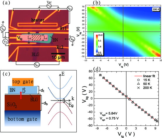
The device geometry, which comprises a heater, two local thermometers (Rt1 and Rt2), three voltages leads and a local top gate as shown in Fig. 1(a), enables the 4-probe measurements of resistance and TEP SOM ; TEPsetup ; CR . The thickness of the hBN micro-crystal for this particular device is 40 nm determined by an atomic force microscope. We note that the top-gate effective region, shown as shaded area in Fig. 1(a), only partially covers the BLG area between voltage leads. Therefore, additional geometric factor needs to be taken into account in order to extract the sheet resistance and TEP for BLG under the top-gate effective region SOM . For the following discussion, we used the suffix e(ne) referring to the top-gate (non)effective region and suffix for the sheet resistance.
Figure 1(b) shows a contour plot for the measured resistance R at 200 K for the device shown in Fig. 1(a). The bottom-gate voltage is swept up to 70 V, while the top-gate voltage is kept at certain value from -10 V to 10V. The high R states occur in regions with large and at opposite polarity defined in Fig. 1(a). When plotting (,) for the peak position of R (Fig. 1(d)), it is nearly temperature independent and shows excellent linearity giving a slope , where and refer to the relative bottom(top)-gate dielectric constant and bottom(top)-gate dielectric thickness, respectively (Fig. 1(c)). Using = 3.9 (), = 300 nm and = 40 nm , we obtained a relative dielectric constant for hBN 4.0 which is in good agreement with the reported value for bulk hBN dean . The introduction of and capacitively changes the carrier density in BLG and hence shifts its chemical potential (). For a given , R attains a peak value whenever is shifted back to CNP by tuning while giving a finite on BLG that grows in magnitude with . The total unscreened displacement field on BLG can be calculated using , where and equal 5.84 V and 0.75 V, respectively, determined from the linear fit shown in Fig. 1(d). Therefore, the large increase in the resistance peak is a direct consequence of the band gap opening (right panel in Fig. 1(c)) due to the inversion symmetry breaking by , which appears to be most dramatic in BLG miyazaki .
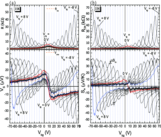
At = 0 and 15 K, R attains a peak value at 5.84 V shown as thick red line in the upper panel of Fig. 2(a). For , the double-peak feature emerges and results from the partial coverage of the top-gate region as mentioned earlier. It is then straightforward to express R = +, where refers to the resistance contribution from top-gate (non)effective region. As increases, the peak value of grows rapidly with its position moving to higher value. At = -8 V, the increase is nearly 9-fold and tends to grow further at higher value. , on the other hand, shows relatively weak dependence on the and can be extracted unambiguously (orange dashed line in Fig. 2(a)). The sheet resistance for the top-gate effective region , where W is the width of BLG, can then be determined as shown in the upper panel of Fig. 2(b). At = 0, the ratio 0.58 is close to the length ratio of as expected (Fig. 1(a)).
The thick red curve in the lower panel of Fig. 2(a) shows the thermoelectric signal as a function of at = 0. is nearly zero at CNP and exhibits ambipolar feature where electron-type (0) and hole-type (0) carriers can be readily tuned by . It increases rapidly in magnitude with attaining local extremes and falls down at higher . Similar to the analysis for resistance, we denoted , where is the thermoelectric signal from the top-gate (non)effective region. When turning on , separates from the thick red curve with local extremes occurring at higher as increase in magnitude as shown in lower panel of Fig. 2(a). The blue curves are signals at that we used for the extraction of the shown as the dashed orange line in the lower panel of Fig. 2(b). However, the ratio of at = 0 turns out to be about 20 % less than the expected ratio of considering the case of an uniform across BLG. This implies a smaller temperature gradient under the top-gate effective region due to a likely heat shunt through the top-gate(Ti-Au)/hBN. By assuming that TEP at zero top-gate voltage is the same throughout the BLG, we can then determine and hence TEP under the top-gate effective region which is shown in the lower panel of Fig.2(b) SOM . At 15 K, the difference between local extremes, denoted as (lower panel in Fig.2(b)), equals 20 V/K and is enhanced by more than 4 folds to 95 V/K and 80 V/K at = -7 V and 8 V, respectively.
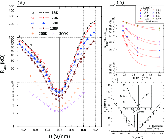
The peak values in log-scale are plotted as a function of the corresponding values at different temperatures shown in Fig. 3(a). The solid symbols that extend to higher are obtained from the same device after cooling down to the base temperature again, which shows consistent behavior. increases exponentially with giving 230 k at 1.2 V/nm and 15 K, which is nearly a 40-fold increase compared to its value at 0 V/nm. However, we notice that the increase in drops slightly for . In order to gain further information on the band gap , we plot the relative conductivity as a function of 100/T for eight different values such that effects other than can be excluded. The data points are then fitted in a temperature range of 50 K-300 K using , where A and C are constants independent of T. The extracted vs. is shown in Fig. 3(c), which is practically linear for 0.3 V/nm giving a 100 meV at -0.9 V/nm close to the value given by infrared microspectroscopy zhang . The data points show good agreement with the calculated band gap (solid line in Fig. 3(c)) using a self-consistent tight-binding model. The fitting function is based on a simplified model of a narrow band-gap semiconductor with impurity band that may originate from disorder and impurity in BLG. The parameter A reflects the dependence of carrier mobility . It turns out to increase with (inset of Fig. 3(c)), where the charge re-distribution (screening) and also change in band structure may play a role.
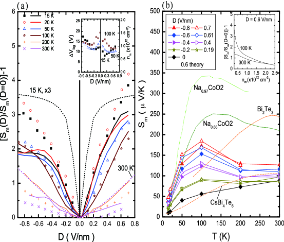
We defined which is the maximum value of . The increase of relative to its value at , , is shown as open symbols in Fig. 4(a). grows larger at lower temperatures and exhibits a minor asymmetry with respect to . At 20 K, reaches a value of 4.2 at = 0.7 V/nm. According to the Mott relation mott , TEP can be described by
| (1) |
where is the electrical conductivity. Using =1/, we can then deduce TEP from the sheet resistance data using according to Eq. 1. The increase of the term with respect to its value at is shown as the solid lines in Fig. 4(a) without any scaling or shifting on them. For T 100K and 0.3 V/nm, we find surprisingly good agreement in the solid lines to the measured values of []-1 (symbols). However, the solid lines starts to deviate downward from the symbols as 0.4 V/nm. Based on the Mott relation, the discrepancy should reflect the dependence of the term that is proportional to the DOS at . We argue that, as increases, more states near CNP are pushed aside forming a band gap that grows wider with . The DOS at the bottom(top) of the conduction(valence) band is then expected to increase with increasing . As shown in the inset of Fig.4(a), , which is the width of the local extremes for measured , equals 12 V at 15 K corresponding to a carrier density at which occurs. The gradual increase of at higher is consistent with the scenario described earlier that may also partly account for the dependence of A in the inset of Fig. 3(c). However, for 200 K and 300 K, the solid lines deviate upward instead. The failure of the Mott relation near CNP at high temperature has also been reported previously by several authors CR ; korea ; shi ; hwang . It was attributed to the violation for the criteria of ( is the Fermi energy), which becomes more pronounced in a cleaner BLG. We note that the enhancement in TEP is mainly associated with the change in band curvature due to rather than that shows relatively weak variation with .
The temperature dependence of at different values is plotted in Fig. 4(b). It exhibits a maximum near 100 K giving a value of V/K. Below 50 K, we remark that ( = 0.7 V/nm), which tends to increase even further at higher , is comparable to the reported large TEP in sodium cobaltates (x=0.97 and 0.88) cobaltate and -based alloys ( CBT and BT ) shown as dotted lines. Unfortunately, the detailed information on thermal conductivity in dual-gated BLG is absent for the determination of thermoelectric figure of merit ZT, where S, , T and are thermoelectric power (TEP), electrical conductivity, temperature and thermal conductivity, respectively snyder . Nevertheless, it was recently pointed out that in encased few-layer graphene can be orders of magnitude smaller due to the quenching of flexual phonon mode flexural1 ; flexural2 ; lau , which makes dual-gated BLG device a potential candidate for large ZT.
Theoretical calculations including the screening effect are based on Kubo’s formula of the linear response coefficients hao . In the clean limit, the predicted relative increase of at 15 K and 300 K are shown as dotted and dashed lines in Fig. 4(a), respectively, which is more than three-fold larger compared to our experimental results. The corresponding is, however, an order of magnitude smaller than the experimental data. We suspect that the presence of charge puddles near CNP can be an important factor, which has been revealed from scanning tunneling microscopy in exfoliated graphene puddle ; puddle2 and BLG leroy on substrate. The effect of electron-hole puddle gives rise to a large charge inhomogeneity puddle ; puddle2 ; tan ; yan near CNP that falls in the same order of magnitude as in our device . The coexistence of electron-type and hole-type carriers at close to CNP is reminiscent of the finite minimum conductivity tan ; zhu ; sarma ; xiao and also phonon-anomaly in bilayer graphene yan . This can also cause a significant compensation in TEP near CNP as suggested in our experiment. We also remark that the relative increase of depends critically on as shown in the inset of Fig. 4(b) obtained from theoretical calculation for at different . The value of inevitably incorporates the impurity doping giving rise to larger impurity scattering at higher and hence a smaller enhancement in TEP.
In conclusion, we demonstrate the electric-field tunable band-gap and TEP in dual-gated BLG device, which may offer a new platform for innovative science and engineering. Unfortunately, large enhancement in TEP only occurs below 100 K in our devices most likely related to the compensation from electron-hole puddles near CNP. It gives (15K, D = 0.7 V/nm)=48 V/K that is comparable to or exceeding existing records for low-T thermoelectric materials. Larger enhancement, in principle, can be realized in a cleaner dual-gated BLG device at higher . With the advantage of full electric field control on TEP and also its carrier polarity, dual-gated BLG device with a proper design can be a promising candidate for low-temperature thermoelectric application.
The authors acknowledge the funding support from National Science Council in Taiwan (NSC99-2112-M-001-032-MY3) and technical support from Core Facility for Nanoscience and Nanotechnology at Academia Sinica in Taiwan.
References
- (1) [] These authors contributed equally to this work. *Electronic address : wlee@phys.sinica.edu.tw
- (2) E. McCann, V. I. Fal’ko, Phys. Rev. Lett. 96, 086805 (2006).
- (3) J. Martin et al., Phys. Rev. Lett. 105, 256806 (2010).
- (4) Y. Barlas, R. Côté, J. Lambert, A. H. MacDonald, Phys. Rev. Lett. 104, 096802 (2010).
- (5) T. Ohta et al., Science 313, 951 (2006).
- (6) E. V. Castro et al., Phys. Rev. Lett. 99, 216802 (2007)
- (7) Y. Zhang et al., Nature 459, 820 (2009).
- (8) H. Miyazaki et al., Nano Lett. 10, 3888 (2010).
- (9) T. Taychatanapat, P. Jarillo-Herrero, Phys. Rev. lett. 105, 166601 (2010).
- (10) D. B. Farmer et al., Nano Lett. 9, 4474 (2009).
- (11) B. Fallahazad. S. Kim, L. Colombo, E. Tutuc, Appl. Phys. Lett. 97, 123105 (2010).
- (12) C. R. Dean et al., Nature Nanotech. 5, 722 (2010).
- (13) See supplementary materials at XXX for details of device fabrication and measurement method.
- (14) L. Hao, T. K. Lee, Phys. Rev. B 81, 165445 (2010); L. Hao, T. K. Lee, Phys. Rev. B 82, 245415 (2010).
- (15) J. P. Small, K. M. Perez, P. Kim, Phys. Rev. Lett. 91, 256801 (2003).
- (16) C. R. Wang, W. S. Lu, W. L. Lee, Phys. Rev. B 82, 121406(R) (2010).
- (17) M. Cutler, N. F. Mott, Phys. Rev. 181, 1336 (1969).
- (18) S. G. Nam, D. K. Ki, H. J. Lee, Phys. Rev. B 82, 245416 (2010).
- (19) D. Wang, J. Shi, Phys. Rev. B 83, 113403 (2011).
- (20) E. H. Hwang, E. Rossi, S. Das Sarma, Phys. Rev. B 80, 235415 (2009).
- (21) M. Lee et al., Nature Mater. 5, 537(2006).
- (22) D. Y. Chung et al., Science 287, 1024 (2000).
- (23) G. J. Snyder, E. S. Toberer, Nature Mater. 7, 105 (2008).
- (24) L. R. Testardi, J. N. Bierly Jr., F. J. Donahoe, J. Phys. Chem. Solids 23, 1209 (1962).
- (25) J. H. Seol et al., Science 328, 213 (2010).
- (26) L. Lindsay, D. A. Broido, N. Mingo, Phys. Rev. B 82, 115427 (2010).
- (27) W. Jang et al., Nano Lett. 10, 3909 (2010).
- (28) J. Martin et al., Nature Phys. 4, 144 (2008).
- (29) Y. Zhang et al., Nature Phys. 5, 722 (2009).
- (30) A. Deshpande et al., Appl. Phys. Lett. 95, 243502 (2009).
- (31) Y. W. Tan et al., Phys. Rev. Lett. 99, 246803 (2007).
- (32) W. Zhu, V. Perebeinos, M. Freitag, P. Avouris, Phys. Rev. B 80, 235402 (2009).
- (33) S. Das Sarma, E. H. Hwang, E. Rossi, Phys. Rev. B 81, 161407(R) (2010).
- (34) S. Xiao et al., Phys. Rev. B 82, 041406(R) (2010).
- (35) J. Yan, E. A. Henriksen, P. Kim, A. Pinczuk, Phys. Rev. Lett. 101, 136804 (2008).


