Factors influencing the distribution of charge in polar nanocrystals
Abstract
We perform first-principles calculations of wurtzite GaAs nanorods to explore the factors determining charge distributions in polar nanostructures. We show that both the direction and magnitude of the dipole moment of a nanorod, and its electic field, depend sensitively on how its surfaces are terminated and do not depend strongly on the spontaneous polarization of the underlying lattice. We identify two physical mechanisms by which is controlled by the surface termination, and we show that the excess charge on the nanorod ends is not strongly localized. We discuss the implications of these results for tuning nanocrystal properties, and for their growth and assembly.
Nanocrystals and nanorods are valued for their unique electronic and optical properties which differ substantially from bulk materials of the same composition smallisdifferent . They are being exploited in a host of applications (including imaging in biology X.Michalet01282005 , light-emitting diodes NirTessler02222002 , lasing devices kazesetal and solar cells Wendy ) that continues to grow in number and diversity as we gain finer control over their properties Nieetal . This requires greater understanding of how those properties depend upon size, shape, internal structure and chemical environment. The distribution of charge within and on a nanorod plays an important role in determining its physical properties: nanostructures with large dipole moments () are sources of large electric fields which, internally, affect their optical properties and, externally, affect their interactions with their surroundings, thereby influencing both their growth and assembly into superstructures shevchenko . The charge distribution is related to the chemical environment and to the conditions of synthesis, however this relationship is not well understood. In this Communication we present first-principles calculations that provide substantial insight into how charge is distributed within a nanocrystal and we identify the most important factors determining this distribution. Our findings can be used to inform the choice of synthesis conditions appropriate for the design of nanorods with specific physical properties.
Much theoretical and experimental work on nanorods has focussed on the magnitude and origin of their dipole moments, with somewhat contradictory results. Some studies attribute large dipole moments to the non-centrosymmetric nature of the wurtzite structure noncentro which is associated with an intrinsic spontaneous polarization – an interpretation that is widely accepted talapin . However a theoretical study has revealed a strong enhancement of the polarity of nanorods compared with thin films of the same length along the direction tsai and experimental observations by Shim and Guyot-Sionnest shim:6955 show that ZnSe nanocrystals with the cubic zincblende structure can exhibit moments of similar magnitude to wurtzite CdSe. Both studies cast doubt on the relevance of crystal symmetry. Other studies have attributed importance to different factors, including nanocrystal shape Shanbhag:2006ix , molecular passivation of surfaces Shanbhag:2006ix ; rabani:1493 , surface reconstruction rabani:1493 ; cicero and a piezoelectric effect caused by strain at the nanocrystal surfaces huong:1769 . Finally, an electrostatic force microscopy study of CdSe nanorods observed no dipole moment in the samples studied PhysRevLett.92.216803 .
Computational modelling of nanorods gives us the control necessary to disaggregate the factors contributing to the dipole moment in a way not possible experimentally. Until recently, nanostructures of realistic sizes have been beyond the reach of accurate quantum-mechanical methods. However, developments in linear-scaling density-functional theory (DFT) methods have now made possible the simulation of nanostructures comprising thousands of atoms with high accuracy. We take advantage of these methods, as implemented in our ONETEP code skylaris:084119 ; PhysRevB.83.195102 , to accurately simulate polar semiconductor nanorods of realistic sizes. For our investigation, we choose nanorods of wurtzite GaAs because GaAs has a relatively low computational cost while having the essential features that bestow all polar nanorods (e.g. CdSe, ZnO) with an asymmetric distribution of charge, namely, there is a degree of ionicity to the bonding and the crystal structure lacks inversion symmetry. This allows us to access the extensive size regime in which a nanorod’s dipole moment increases linearly with its length and width.
Our results highlight the importance of surface chemistry to the distribution of charge in polar semiconductor nanorods and show that the symmetry of the corresponding bulk crystal structure can play a much less important role than has often been assumed. Indeed, for some surface terminations, can be in the opposite direction to that suggested by the spontaneous polarization of the bulk crystal. We show that excess charge on the ends of a nanorod can be highly delocalized, meaning that internal electric fields are non-uniform and that some simple models of electrostatic interactions between nanoparticles may be overly simplistic. We explain the relationships that we find between the surface terminations of a nanorod and its dipole moment in terms of the electronic structure. Finally, we show that our findings are robust when the atomic structure is allowed to relax.
The ONETEP code uses DFT in a formulation equivalent to the plane-wave pseudopotential method RevModPhys.64.1045 . Initially we model unrelaxed, stoichiometric nanorods of wurtzite (w-) GaAs. Our nanorods are ‘grown’ parallel to the wurtzite -axis with a length nm and hexagonal cross-sections of width nm: an example is shown in Fig. 1.

Six different nanorods consisting of 2106–2862 atoms were created to represent a variety of lateral () and polar () surface terminations, either bare or saturated by chemisorption. They are labelled H/H, H/B, H/P, B/H, B/B, B/P, to indicate how the lateral/polar surfaces are terminated, respectively. H signifies termination by hydrogen atoms and B signifies a bare surface. P denotes termination by pseudo-atoms PhysRevB.71.165328 , each with one electron and fractional nuclear charges of and for passivating surface Ga and As atoms respectively. By approximating the electronegativities of As and Ga they form bonds with the surface atoms of similar character to those found in the bulk and render the III-V semiconductor surfaces electronically inert PhysRevB.71.165328 without contributing any net charge to them. A H atom, on the other hand, passivates a surface dangling bond but also contributes a net negative (positive) charge of magnitude to the surface when it binds to a Ga (As) atom. In all of these models symmetry dictates that only the longitudinal component of , , is non-zero.
A plane-wave energy cut-off of 450 eV, with a local orbital radius 0953-8984-17-37-012 of 0.53 nm for each atomic species is found to be sufficient to converge all properties of interest. The density kernel is not truncated so that metallic and insulating structures are treated on an equal footing. We use norm-conserving pseudo-potentials with non-linear core corrections, and 3d electrons frozen into the core. Exchange and correlation are treated within the local density approximation. To eliminate interaction between a nanorod and its periodic images we have used a cylindrically truncated Coulomb interaction PhysRevB.73.205119 .
Table 1 shows that both the magnitude and direction of depend critically on the chemistry of both the lateral and polar surfaces and therefore cannot be dominated by the spontaneous polarisation of the wurtzite lattice. We have calculated this quantity for bulk w-GaAs to be 0.005 C/m2, implying a contribution to for nanorods of our size of +62 D, if the polarizations are similar cicero . H/B and B/B both show positive , meaning that the Ga-terminated end carries a net positive charge, while B/P has a very small and the other rods exhibit negative . These observations suggest that the synthesis conditions of nanorods and their chemical environments must play crucial roles in determining , insofar as they affect the coverage of the surfaces with adsorbates.
| Nanorod | H/H | H/B | H/P | B/H | B/B | B/P | ||||||
|---|---|---|---|---|---|---|---|---|---|---|---|---|
| (D) | -614 | +330 | -531 | -235 | +125 | +41 | ||||||
| (e) | +1. | 00 | -0. | 56 | +0. | 95 | +0. | 39 | -0. | 18 | -0. | 08 |
| (V/nm) | -0. | 100 | +0. | 050 | -0. | 105 | -0. | 030 | +0. | 013 | +0. | 005 |
Figure 2 shows the calculated of nanorods with fully H-terminated lateral surfaces, but with a varying coverage of H atoms on the polar surfaces. Each point represents a single sample chosen at random from the ensemble of nanorods with a given coverage. It is clear that tends to decrease significantly as the hydrogen coverage increases and that changes direction around 56% coverage. This means that if one could control the degree of coverage of the polar surface (e.g. by varying the temperature, pressure, or the chemical potentials of the various species during synthesis) one could vary over a wide range of values. At K, we have calculated that over the range of realistic hydrogen chemical potentials for which water molecules are stable, the thermodynamically stable hydrogen coverage, namely that which minimises , goes from 0 to around 70%. In principle, this therefore allows access to values of of between -200 D and +330 D. Even at full coverage, if there were competing adsorbing species, we suggest that could be tuned by varying their proportions. Indeed, terminating each of the polar surfaces with 13 H and 14 pseudo-atoms yields D, between H/H and H/P.

In Fig. 3(a) we plot the function
which is the laterally-averaged charge density profile along the length of the nanorod (the direction in this work, ), convolved with a Gaussian of standard deviation nm in the direction. This smooths out the large variations in the density on the length scale of a unit cell, revealing how excess charge is distributed along the length of the nanorod: clearly it is spread over several nm from the ends of the nanorods. The amount of excess charge on the left-hand (As-terminated) end, , is shown in Table 1. This has been calculated by integrating the quantity up to the middle of the nanorod.
The observed spread of the excess charge could be important for models of nanoparticle self-assembly that usually treat nanocrystals as point dipoles or assume that excess charge is perfectly localized on the polar surfaces shevchenko ; talapin These assumptions would lead to quantitatively, or even qualitatively, incorrect results at short distances. Furthermore, the delocalization of charge suggests that nanorods may be highly polarizable, which could significantly affect the interactions between nanorods.
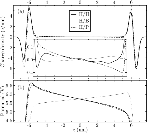
Figure 3(b) shows the smoothed potential as a function of position along three different nanorods and Table 1 gives the values of the electric field at the centre of each nanorod, . It is clear that the internal electric fields are not uniform but stronger near the polar surfaces than in the middle. The voltage drops we have observed are of order 0.1 V/nm, reaching as high as 0.6 V/nm near the polar surfaces of H/H. These fields are of similar magnitude to those observed in strained quantum wells and are expected to significantly affect optical absorption frequencies, selection rules and carrier recombination rates.
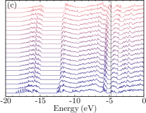
Figure 4 shows the calculated ‘slab-wise’ local densities of states (LDOS) for nanorods H/H, H/B, and B/H. We define a slab LDOS as follows: each nanorod is nominally divided into 20 slabs in the -direction, each consisting of four planes of atoms: two each of Ga and As. The slab LDOS is the sum of the contributions to the total DOS from the local orbitals centred on those atoms. Superposing these slab LDOS, as in Fig. 4, shows that the electric field shifts the spectrum from slab to slab. This shift has the effect of smearing out the total DOS so that none of the nanorods studied has an electronic energy gap despite individual slabs having well-defined gaps.


Closer examination of Table 1 reveals two distinct trends: first, that all other things being equal, terminated polar surfaces result in the most negative , and bare polar surfaces result in the most positive. Second, terminated lateral surfaces result in of larger magnitude than bare lateral surfaces.
Figure 4 helps us to understand these trends: polar surface dangling bond states on H/B can clearly be identified in Fig. 4(b) on the data sets associated with the first and last slabs of the nanorod. The Ga (As) dangling bond states lie mostly above (below) the Fermi level , resulting in an excess of electrons on the As-terminated end and a more positive . In contrast, Fig. 4(a) reveals that both the Ga-H and As-H bonding states on the polar surfaces of H/H lie below , resulting in an excess of electrons on the Ga-H terminated end and a depletion on the As-H end. This is because the of an electron nominally available from the Ga atom, and the one electron available from H are insufficient to fully populate the Ga-H bond. Conversely, the electrons from As provide a surplus for the As-H bond. Hence the formation of these bonds redistributes charge between the two polar surfaces to produce a negative . In real systems, a mechanism is required to redistribute charge between two distant end surfaces, such as the presence of a solvent capable of mediating the transfer.
Regarding the second trend: comparison of Figs. 4(a) and 4(c) shows that the nanorod with bare lateral surfaces (B/H) does not exhibit a large local energy gap as H/H does due to the presence of lateral surface dangling bond states. A large is associated with a large internal electric field and slab-by-slab energy shift. However, for nanorods with lateral surface states close to , the electric field pushes these states above at one end and below at the other thereby reversing the charge build up on the ends and reducing the field. We conclude from these observations that a large local energy gap clear of surface states is a necessary condition for a large , and the quenching of surface states on unstable lateral surfaces, by the introduction of adsorbates, can be an important polarity enhancement mechanism in nanorods.
So far we have considered pristine nanorods. However, structural relaxations might be expected to play a large role for two reasons: some of the surfaces studied above may be unstable and, given our arguments above, reconstructions are likely to have a large effect; strain caused by the surface may also induce significant charge separation. Regarding the first concern, it has not been our intention here to determine the stability of a particular surface, but rather to investigate the link between termination and , regardless of stability. Secondly, to assess the effects of surface-induced strain we performed structural relaxations on four nanorods of length nm, width nm and with different surface terminations (b/b, h/b, h/h, b/h, following the same convention as before). Table 2 shows before and after structural relaxation: there is no qualitative change in any of the values except b/h. No dipole moments changed direction, and the ordering of the magnitudes stayed the same. The increase in on b/h is attributable to the shifting of the lateral surface dangling bond states away from on relaxation, opening up the energy gap and, consistent with the argument above, supporting a larger .
| Nanorod | h/h | h/b | b/h | b/b | |||||||
|---|---|---|---|---|---|---|---|---|---|---|---|
| before | relaxation | -131. | 64 | +55. | 20 | -22. | 81 | +15. | 38 | ||
| after | (D) | -103. | 03 | +67. | 99 | -89. | 23 | +21. | 52 | ||
In summary, we find that for polar nanorods both the orientation and magnitude of the dipole moment depend sensitively on the chemical terminations of both the polar end surfaces and the non-polar lateral surfaces. This sensitivity can overwhelm any contribution that may arise from the non-centrosymmetric crystal structure. The sensitivity to adsorbates arises in two main ways: adsorbates may be charged and therefore contribute directly to ; they also determine the stability of surface electronic states which, in turn, determines the magnitude of the internal electric field that a rod can sustain. When the electric field becomes large enough to shift the energy of an unoccupied state on one end above an occupied state on the other, a transfer of electrons between the ends occurs that lowers , as long as such a transfer can be facilitated by the environment. The synthesis conditions and environment of a nanorod therefore play crucial roles in determining both the ground state charge distribution of a nanorod and whether or not it can reach this ground state. We also find that surface charge is not localized at the ends of the nanorod but delocalized over several nanometers, also implying an non-uniform internal field. This has implications when considering the energetics of self assembly of polar nanostructures.
This work was supported by EPSRC (UK) under Grant No. EP/G05567X/1,
the EC under Contract No. MIRG-CT-2007-208858 and a Royal Society
University Research Fellowship (PDH). All calculations were run on the
Imperial College HPC Service.
∗ Corresponding author; email: p.tangney@imperial.ac.uk.
References
- (1) M. A. El-Sayed, Accounts Chem. Res. 37, 326 (2004).
- (2) X. Michalet et al., Science 307, 538 (2005).
- (3) N. Tessler et al., Science 295, 1506 (2002).
- (4) M. Kazes et al., Adv. Mater. 14, 317 (2002).
- (5) W. U. Huynh, J. J. Dittmer and A. P. Alivisatos, Science 295, 2425 (2002).
- (6) Z. Nie, A. Petukhova and E. Kumacheva, Nat. Nanotechnol. 5, 15 (2010).
- (7) E. V. Shevchenko et al., Nature 439, 55 (2006).
- (8) T. Nann and J. Schneider, Chem. Phys. Lett. 384, 150 (2004); L.-S. Li and A. P. Alivisatos, Phys. Rev. Lett. 90, 097402 (2003); S. A. Blanton et al., Phys. Rev. Lett., 79, 865 (1997); E. Rabani et al., J. Chem. Phys. 110, 5355 (1999).
- (9) D. V. Talapin et al., Nano Lett. 7, 1213 (2007).
- (10) M. -H. Tsai et al., App. Phys. Lett. 89, 203101 (2006).
- (11) M. Shim and P. Guyot-Sionnest, J. Chem. Phys. 111, 6955 (1999).
- (12) S. Shanbhag and N. A. Kotov, J. Phys. Chem. B 110, 12211 (2006).
- (13) E. Rabani, J. Chem. Phys. 115, 1493 (2001).
- (14) G. Cicero, A. Ferretti and A. Catellani, Phys. Rev. B 80, 201304 (2009).
- (15) N. Q. Huong and J. L. Birman, J. Chem. Phys. 108, 1769 (1998).
- (16) R. Krishnan et al., Phys. Rev. Lett. 92, 216803 (2004).
- (17) M. C. Payne et al., Rev. Mod. Phys. 64, 1045 (1992).
- (18) C.-K. Skylaris et al., J. Chem. Phys. 122, 084119 (2005).
- (19) N. D. M. Hine et al., Phys. Rev. B 83, 195102 (2011).
- (20) X. Huang, E. Lindgren and J. R. Chelikowsky, Phys. Rev. B 71, 165328 (2005).
- (21) C.-K. Skylaris et al., J. Phys.: Condens. Matter 17, 5757 (2005).
- (22) C. A. Rozzi et al., Phys. Rev. B 73, 205119 (2006).