Optical Modulation Effects on Nonlinear Electron Transport in Graphene in Terahertz Frequency Range
Abstract
We describe very fast electron dynamics for a graphene nanoribbon driven by a control electromagnetic field in the terahertz frequency regime. The mobility as a function of bias field has been found to possess a large threshold value when entering a nonlinear transport regime. This value depends on the lattice temperature, electron density, impurity scattering strength, nanoribbon width and correlation length for the line-edge roughness. An enhanced electron mobility beyond this threshold has been observed, which is related to the initially-heated electrons in high energy states with a larger group velocity. However, this mobility enhancement quickly reaches a maximum governed by the Fermi velocity in graphene and the dramatically increased phonon scattering. Super-linear and sub-linear temperature dependences of the mobility are seen in the linear and nonlinear transport regimes, which is attributed separately to the results of sweeping electrons from the right Fermi edge to the left one through elastic scattering and moving electrons from low-energy states to high-energy ones through field-induced electron heating. The threshold field is pushed up by a decreased correlation length in the high field regime, and is further accompanied by a reduced magnitude in the mobility enhancement. This implies an anomalous high-field increase of the line-edge roughness scattering with decreasing correlation length due to the occupation of high-energy states by field-induced electron heating. Additionally, a self-consistent device modeling has been proposed for graphene transistors under an optical modulation on its gate, which employs Boltzmann moment equations up to the third order for describing fast carrier dynamics and full wave electromagnetics coupled to the Boltzmann equation for describing spatial-temporal dependence of the total field. Finally, a detailed comparison of the derived Maxwell-Boltzmann moment equations in this paper with the well known Vlasov-Maxwell equations is also included.
I Introduction
The engineering achievement of isolating graphene sheets art10 ; art11 ; art12 ; philtrans from graphite has inspired many studies aimed at understanding basic underlying physics art10 ; neto as well as finding possible applications to carbon-based electronics art13 . The low-field linear transport of charge carriers in a graphene layer, has received a considerable amount of attention. art1 ; art2 ; art3 ; art4 ; art5 ; art7 ; art8 Recent reports on the successful fabrication of ultra-fast graphene transistors art14 and photodetector art15 has further advanced this research frontier into the fields of electronics and optoelectronics. The graphene transistor was reported to be used as both an electrical modulator modulator with a frequency as high as GHz and as a sensitive photo-detector for imaging detector . However, similar investigations of linear transport in graphene nanoribbons (GNRs) have only been given relatively little attention so far. art6 ; fang ; art9
Early theoretical studies art7 ; fang on electron transport in graphene nanoribbons were restricted to the low-field regime, where a linearized Boltzmann equation was solved within a relaxation-time approximation. In this paper, the non-equilibrium distribution of electrons is calculated exactly by solving the Boltzmann transport equation beyond the relaxation-time approximation for nonlinear electron transport in semiconducting graphene nanoribbons. Enhanced electron mobility from initially-heated electrons in high energy states is anticipated. An anomalous increase in the line-edge roughness scattering for large electric fields is obtained with decreasing roughness correlation length due to the occupation of high-energy states by field-induced electron heating. The semi-classical Boltzmann transport equation is expected to be applicable to the diffusive band-transport regime with relative smooth edges for graphene nanoribbons, instead of the hopping and tunneling between localized states with rough edges.
Macroscopic simulation of semiconductor device physics has proceeded with solving coupled Maxwell -Boltzmann equations. matt-1 ; matt-2 By employing the quasi-equilibrium Fermi-Dirac distribution in the Boltzmann transport equation, we can obtain the spatial dependence of both chemical potential and temperature, which paves the ground for drift-diffusion and hydrodynamic charge transport theories. matt-2 ; matt-3 An ensemble of interacting electrons can be thermalized quickly with a high density, which justifies the assumption of a quasi-equilibrium Fermi-Dirac distribution for hot carriers. To determine the spatial dependence of chemical potential and temperature, device simulators usually couple Maxwell equations for the electromagnetic fields to conservation relations for carrier density, the current and energy. Several investigations on hydrodynamics are related to determining the proper mathematical representation of carrier thermal conductivity and the moments of the Boltzmann equation. matt-2 ; matt-12 ; matt
The outline of the remainder of this paper is as follows. In Sec. II.1, we solve exactly the semi-classical Boltzmann transport equation for low-temperature electron transport in semiconducting graphene nanoribbons by including impurity, line-edge roughness and phonon scattering effects at a microscopic level. Based on the calculated non-equilibrium distribution as a function of wave number along the ribbon, we present detailed numerical results for the electron mobility as a function of either the applied electric field or the lattice temperature for various impurity scattering strengths and correlation lengths for line-edge roughness. Our numerical results are presented in Sec. II.2 with some discussions. In Sec. III.1, we derive the moment equations from the Boltzmann equation up to the third order for electron dynamics in doped graphene as a generalization to hydrodynamic model. At the same time, the self-consistent field equations are also derived in Sec. III.2 within the Maxwell-Boltzmann frame. Finally, the conclusions of this paper are presented in Sec. IV.
II Nonlinear Transport in Graphene Nanoribbons
In this section, we employ the Boltzmann transport model with inclusion of scattering at a microscopic level to study high-field nonlinear transport of electrons in graphene nanoribbons along with some numerical results.
II.1 Nonlinear Boltzmann Transport Model
Here, we investigate single subband nonlinear transport only in the armchair nanoribbon (ANR) configuration wakabayashi . Low electron densities, moderate temperatures, ionized impurities and line-edge roughness are considered fang ; huang1 ; huang2 . As a result, negligible pair scattering pair , optical and out-of-plane flexural phonons huang2 , inter-valley scattering, volume-distributed and short-range impurity scattering fang will all be neglected. Therefore, the electron-like branch for doped graphene can be represented on a space mesh, neto via its dispersion and corresponding wave-function, as
| (1) | |||
| (4) |
Here, m/s is the Fermi velocity in graphene and is the quantization length of the ribbon. For semiconducting ANR, is the quanta of the transverse wave vector and is the phase separation between the two graphene sublattices. The electron wave numbers are given on the discrete mesh by for large odd integer , is a small mesh spacing, and is chosen to ensure that scattering induced population of higher electron-like branches can be neglected. The minimum in the energy dispersion curve corresponds to the central mesh point . Also, is the width of a ribbon expressed in units of the size of graphene unit cell Å and the number of carbon atoms across the ribbon. According to the dispersion relation in Eq. (1), the electron group velocity for semiconducting ANRs is given by . Additionally, we assume that the electron-like branch is filled up to at zero temperature with the Fermi wave number and energy given by and , respectively. For a chosen temperature and chemical potential , the linear electron density in ANR follows from , with being the equilibrium Fermi-Dirac distribution function.
Conventionally, the non-equilibrium carrier distribution function is partitioned as . The deviation from the equilibrium Fermi distribution under a strong electric field is described by the set of reduced nonlinear Boltzmann transport equations huang1 ; huang2
| (5) |
In this notation, is the reduced form of the dynamical non-equilibrium part fn2 of the electron distribution function. The reduced form accounts for particle number conservation condition, i.e., . Reduced scattering matrix elements are defined via its components
| (6) | |||||
Here, the elastic scattering rate is given by:
| (7) |
where denotes the impurity scattering rate at the Fermi edges and . Since the momentum difference between two valleys is rather large, only short-range impurities (such as topological defects) with a range smaller than the lattice constant will give rise to inter-valley scattering. is the scattering rate due to edge roughens, with Å being the amplitude and being the correlation length of the roughness.
The dominating inelastic scattering mechanism is provided by longitudinal acoustic phonons at low temperatures. The static inelastic scattering rates are given by the following matrix elements
| (8) | |||||
| (9) |
Here, , , , is the Bose-Einstein function for thermal equilibrium phonons; eV is the deformation potential, g/cm2 and cm/s are the mass density and sound velocity in graphene. The scattering potentials are screened by free carriers and described by a dielectric function. Here, we assume that the inelastic scattering is shielded by the static Thomas-Fermi dielectric function in its general form fang ; fertig1 . The screening of elastic scattering potentials is given approximately by under the metallic limit () with .
The nonlinear dynamical phonon scattering rate is
| (10) |
which is also responsible for the nonlinear electron transport and electron heating due to its dependence on .
Once the non-equilibrium part, , of the total electron distribution function has been determined using Eq. (5), the transient drift velocity, , of the system can be calculated with the use of
| (11) |
We note that the thermal-equilibrium part of the electron distribution does not contribute to the drift velocity. The steady-state drift velocity of electrons is given by by taking the limit . The corresponding steady-state conduction current is given by . The differential electron mobility for nonlinear transport is generalized to . Numerical simulation of these quantities in specific ANRs is presented below.
II.2 Numerical Results and Discussion
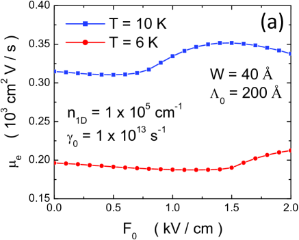
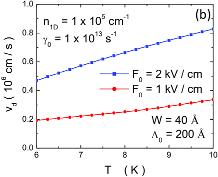
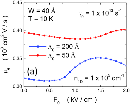
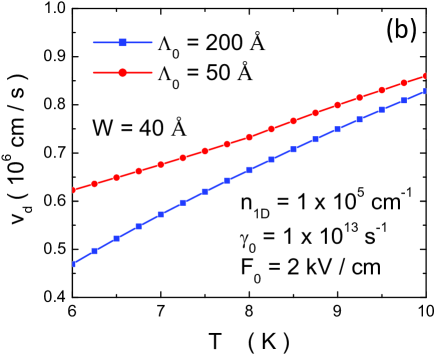
Figure 1(a) presents our calculated electron mobilities as a function of applied electric field at K (blue curve) and K (red curve), respectively. Clearly, from Fig. 1(a), a strong -dependence for appears at a lower value of at higher temperature in the nanoribbon. This -dependent electron mobility has its physical origins in the dynamical electron-phonon scattering rate through its dependence on the electron distribution function given in Eq. (10). Consequently, it is reasonable to expect a lower threshold field, , for entering into a nonlinear transport regime () due to enhanced nonlinear phonon scattering at K. The value of strongly depends on the parameters of the system, such as , , and , and an analytic expression for cannot be obtained in the nonlinear transport regime. On the other hand, as , is larger at K than K due to thermal population of high-energy states with a large electron group velocity. The initial decrease of with is attributed to the gradual increase of the frictional force from phonon scattering by . At K, is roughly independent of below kV/cm (linear regime). However, increases significantly with above kV/cm (nonlinear regime). Eventually, decreases with once it exceeds kV/cm (heating regime), leading to a saturation of the electron drift velocity. The electron group velocity increases with the wave number for small values, as can be seen from Eq. (1). However, the increase of slows down toward its upper limit provided but still within the single-subband regime. The increase of with in the nonlinear regime comes from the initially-heated electrons in high energy states with a larger group velocity, while the successive decrease of in the heating regime comes from the combination of the dramatically increased phonon scattering and the upper limit mentioned above. In Fig. 1(b), the calculated electron drift velocities are plotted as a functions of temperature when kV/cm (blue curve) and kV/cm (red curve). The fact that increases with monotonically in both cases implies the electron scattering in two samples is not dominated by phonons but by impurities and line-edge roughness. Different behaviors in the increase of with temperature can be seen from Fig. 1(b) for linear and nonlinear electron transport. At kV/cm for the high-field nonlinear transport, (or ) increases with sub-linearly. On the other hand, rises super-linearly with for the low-field linear transport at kV/cm. These different dependence in for linear and nonlinear transports can be directly related to the non-equilibrium part of the electron distribution function .
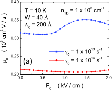
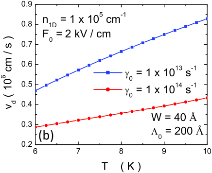
The effects due to impurity scattering are compared in Figs. 2(a) and 2(b). In Fig. 2(a), we present a comparison of mobilities as a function of at K for s-1 (blue curve) and s-1 (red curve). As , is greatly reduced by strong impurity scattering with s-1 in the linear regime. In addition, for s-1, is pushed upward from about kV/cm to kV/cm, leaving us with a roughly -independent in this case for the whole field range shown in this figure. The comparison for -dependence of is presented in Fig. 2(b) for kV/cm, where a sub-linear increase of with for weak impurity scattering is switched to a super-linear relation in the strong impurity scattering case.
Finally, the effect of correlation length for the line-edge roughness on the transport is demonstrated in Figs. 3(a) and 3(b) by fixing Å and changing from Å to Å. As shown in Eq. (7), the line-edge roughness scattering can be either reduced or enhanced by decreasing , depending on or . For our chosen sample with cm-1, we find that the condition is satisfied in the low-field limit (), while holds for the high field limit due to electron heating. Therefore, we find from Fig. 3(a) that is increased as when is reduced to Å in the low field regime. However, the value of for is pushed upward for Å in the high-field regime, which is further accompanied by a reduced magnitude in the enhancement of with . This anomalous feature associated with reducing also has a profound impact on the -dependence of as shown in Fig. 3(b), where the increasing rate of with in the high field regime becomes much lower with Å than for Å.
III Optical Modulation to Graphene Layers
In this section, we will first derive the Boltzmann moment equations up to third order in describing very fast electron dynamics driven by a control electromagnetic field in the terahertz frequency regime. At the same time, a self-consistent equation is also derived for the total driven field, including the induced optical coherence in a graphene layer.
III.1 Boltzmann Moment Equations
For electrons in a two-dimensional doped conducting graphene layer with its band structure given by a Dirac cone, the Boltzmann equation for the electron distribution function around (or ) valley point is
| (12) |
where is the group velocity of Bloch electrons with kinetic energy and the Fermi velocity cm/s . The Newton’s second law requires that with , and being the electron charge, in-plane electrical and static magnetic fields, respectively. refers to the electric component of the total electromagnetic field, which should be determined by the self-consistent field equation (see next subsection below). The Markovian collision term introduced in Eq. (12) is
| (13) |
where and are the scattering-in and scattering-out rates for electrons in the two-dimensional -state. Based on the Newton’s second law, we rewrite Eq. (12) into the form of
| (14) |
The zeroth-order moment of the Boltzmann equation in Eq. (14) is found from
| (15) |
which leads to the following electron number conservation equation, after the inter-valley scattering is ignored,
| (16) |
where is the sample area, is the electron sheet number density (per area) and is the electron surface number current density (per length). Equation (16) allows us to determine the the spatial distribution of at each time .
In order to simplify the first-order moment of the Boltzmann equation, we introduce the momentum-relaxation time approximation. Under this approximation, we write
| (17) |
where is the Fermi-Dirac function for thermal-equilibrium electrons and is the average momentum-relaxation time for electrons. In principle, can be microscopically calculated based on introduced in Eq. (6) in the previous section for fixed applied bias and temperature as well as device parameters. In addition, we introduce the force-balance equation, which yields
| (18) |
This leads to, to the leading order of a weak field with ,
| (19) |
Employing the result in Eq. (17), we arrive at the first-order moment of the Boltzmann equation
| (21) |
It is straight forward to show for each valley that
| (22) |
| (23) |
where , , and the dimensionless function
| (24) |
The local chemical potential can be calculated from Eq. (22) if both and are given. Based on the results in Eqs. (22) and (23), we finally get the generalized drift-diffusion equation
| (25) |
Equation (25) enables us to determine the spatial distribution of the electron number current density at each time . The Einstein relation can be obtained by setting and in Eqs. (16) and (25) for a steady state, i.e. , which relates the diffusion current to the external electric field . In addition, by setting as a constant, Equations (15) and (25) constitute the basic hydrodynamic equations for and . Although the particle number conservation is enforced in this way, the energy of the system is not conserved in general.
The second-order moment of the Boltzmann equation is formally written as
| (27) |
where is the lattice temperature, and can be evaluated using the calculated non-equilibrium part of electron distribution as well as in Eq. (6) for fixed applied bias field, temperature and device parameters. This leads Eq. (26) to the following electron power loss equation
| (28) |
where the second and last terms on the right-hand-side of this equation corresponds to thermal energy exchange with lattice and Joule heating, is the average kinetic energy of electrons per area, and is the electron surface energy flux per length. It is easy to show that
| (29) |
By substituting Eq. (29) into Eq. (28), this lets us find the spatial distribution of the electron temperature at each time .
To simplify the third-order moment of the Boltzmann equation, we still employ the momentum-relaxation time approximation in Eq. (17). This leads to
| (31) |
From Eq. (31), we are able to calculate the spatial distribution of the electron energy flux at each time , from which the electron thermal conductivity can be obtained.
Now let us summarize our findings in this subsection by presenting the complete set of equations describing the moments of the Boltzmann equation. Since Dirac electrons posses non-parabolic energy dispersion, the relevant moments are written as the powers of both energy and group velocity, i.e.
where has the meaning of electron density, is the sheet current density, is the average electron kinetic energy, and is the electron surface energy flux. The above moments are augmented with the electron temperature . Based on two calculated moments and , the momentum (or the group velocity) can be determined from the force-balance equation, i.e. , where the momentum relaxation-time () approximation has been employed. In general, the total force , including the resistive force from electron scattering, must be found from the Maxwell equations. This point is further elucidated in the next paragraph. Note that the simultaneous solution of the Boltzmann-Maxwell equations is known as the Vlasov-Maxwell equation vlasov , which can be used to elevate the relaxation-time approximation including the long-range Coulomb interaction. Our approach in this paper still retains the essence of the Maxwell equations but simplifies their introduction into the Boltzmann equation by means of the force-balance equation. As a result of this, it leaves us with the momentum and energy () relaxation times in the formalism. This partial simplification of the Vlasov-Maxwell equations gives rise to the correct treatment of electron transport driven by a terahertz optical field.
The system of equations for the moments is given by
| (32) | |||
| (33) | |||
| (34) | |||
| (35) |
where . As mentioned before, these equations are intertwined with the Maxwell equations if one aims to look for the self-consistent response of Dirac plasma to an incident optical field. Another approach would be studying the ideal magneto-hydrodynamics of the plasma, which can be applied to the case when magnetic lines are frozen into an electron plasma. Formally, this corresponds to a vanishing total force () and to a decoupling of the moments equations. Once those moments are obtained, it would provide the electromagnetic field inside the Dirac plasma via Maxwell equations as described in the next subsection.
III.2 Self-Consistent Field Equation
The Maxwell equations for the transverse magnetic component with , as well as for the electric component with , are given by
| (36) |
| (37) |
where is the relative dielectric constant of embedded host materials including the gate oxide material and induced optical polarization field. The calculations of these four equations can be performed by using the Delaunay-Voronoi surface integration scheme. cell The total electromagnetic fields, and , are coupled to the moments of the Boltzmann equation through the following boundary conditions for at the two-dimensional graphene sheet ()
| (38) |
| (39) |
| (40) |
where is the ion sheet density, and the total charge neurility requires that
| (41) |
Here, the Maxwell equations must be solved self-consistently with the Boltzmann moment equations in the previous subsection. last In addition, we have continuity conditions at the boundary
| (42) |
| (43) |
In Eq. (38), , which produces a space-charge field, is the induced surface charge density by a gate voltage . For the graphene transistor structure, we also require that and , where we assume that the conduction channel is in the direction with a channel length and represents the applied source-drain ac voltage. Also, represents the gate electrode depth.
IV Concluding Remarks
In conclusion, we have found there is a minimum electron mobility for a graphene nanoribbon just before a threshold for an applied electric field when entering into the nonlinear transport regime, which is attributed to the gradual build-up of a frictional force from phonon scattering by the applied field. We also predict a field-induced mobility enhancement right after this threshold value, which is regarded as a consequence of initially-heated electrons in high energy states with a larger group velocity in an elastic-scattering dominated graphene nanoribbon. Moreover, we have discovered that this mobility enhancement reaches a maximum in the nonlinear transport regime as a combined result of an upper limit for the carrier group velocity in a nanoribbon and a field-induced dramatically-increased phonon scattering in the system. Finally, the threshold field can be pushed upward and the magnitude in the mobility enhancement can be reduced simultaneously by a small correlation length for the line-edge roughness in the high-field limit due to the occupation of high-energy states by field-induced electron heating.
Additionally, we have formulated a self-consistent device simulation for graphene transistors in the presence of field modulation within the terahertz frequency range. This involves moment equations from the Boltzmann equation up to the third order for fast carrier dynamics, as well as full wave electromagnetics coupled to the Boltzmann equation for describing both temporal and spatial dependence of the total field including the induced optical polarization field.
When the electron density is increased in a graphene nanoribbon, multi-subband transport occurs, the field-induced mobility enhancement is expected to be reduced, and the effect of electron-electron scattering needs to be included. When the lattice temperature becomes high, on the other hand, neither the optical phonon nor inter-valley scattering should be neglected. As the width of a nanoribbon is modulated, a periodic potential along the ribbon will form, leading to a graphene nanoribbon super-lattice with additional mini-band gap opening at the Brillouin zone boundaries. The results of the current research is expected to be very useful for our understanding and design of high-power and high-speed graphene nanoribbon emitters and detectors in the terahertz frequency range.
Acknowledgement(s)
This research was supported by contract # FA 9453-07-C-0207 of AFRL. DH would like to thank the Air Force Office of Scientific Research (AFOSR) for its support. DH would also like to thank Prof. Xiang Zhang for hosting the Visiting Scientist Program sponsored by AFOSR.
References
- (1) A. K. Geim and K. S. Novosolev, Nat. Mater. 6, 183 (2007).
- (2) K. S. Novosolev, A. K. Geim, S. V. Morozov, D. Jiang, M. I. Katsnelson, I. V. Grigorieva, S. V. Dubonos, and A. A. Firsov, Nat. (London) 438, 197 (2005).
- (3) C. Berger, Z. Song, X. Li, X. Wu, N. Brown, C. Naud, D. Mayou, T. Li, J. Hass, A. N. Marchenkov, E. H. Conrad, P. N. First, and W. A. de Heer, Sci. 312, 1191 (2006).
- (4) O. Roslyak, Godfrey Gumbs, and D. H. Huang, Phil. Trans. A
- (5) A. H. C. Neto, F. Guinea, N. M. R. Peres, K. S. Nonoselov, and A. K. Geim, Rev. Mod. Phys. 81, 109 (2009).
- (6) P. Avouris, Z. Chen, and V. Perebeinos, Nat. Nanotechnol. 2, 605 (2007).
- (7) T. Ando, J. Phys. Soc. Jpn. 75, 074716 (2006).
- (8) J. H. Chen, C. Jang, S. Adam, M. S. Fuhrer, E. D. Williams, and M. Ishigami, Nat. Phys. 4, 377 (2008).
- (9) H. M. Dong, W. Xu, Z. Zeng, T. C. Lu, and F. M. Peeters, Phys. Rev. B77, 235402 (2008).
- (10) N. M. R. Peres, J. M. B. Lopes dos Santos, and T. Stauber, Phys. Rev. B76, 073412 (2007); also see T. Stauber, N. M. R. Peres, and F. Guinea, ibid. 76, 205423 (2007).
- (11) V. V. Cheianov and V. I. Falḱo, Phys. Rev. Lett. 97, 226801 (2006).
- (12) W. Xu, F. M. Peeters, and T. C. Lu, Phys. Rev. B79, 073403 (2009).
- (13) S. Y. Liu, X. L. Lei, and N. J. M. Horing, J. Appl. Phys. 104, 043705 (2008).
- (14) Y.-M. Lin, C. Dimitrakopoulos, K. A. Jenkins, D. B. Farmer, H.-Y. Chiu, A. Grill, and P. Avouris, Sci. 327, 662 (2010).
- (15) T. Mueller, F. Xia, and P. Avouris, Nat. Photonics 4, 297 (2010).
- (16) Y.-M. Lin, K. A. Jenkins, A. Valdes-Garcia, J. P. Small, D. B. Farmer, and P. Avouris, Nano Lett. 9, 422 (2009).
- (17) F. Xia, T. Mueller, R. Golizadeh-Mojarad, M. Freitag, Y-M. Lin, J. Tsang, V. Perebeinos, and P. Avouris, Nano Lett. 9, 1039 (2009).
- (18) Y.-M. Lin, V. Perebeinos, Z. Chen, and P. Avouris, Phys. Rev. B78 161409 (2008).
- (19) T. Fang, A. Konar, H. Xing, and D. Jena, Phys. Rev. B78, 205403 (2008).
- (20) X. Wang, Y. Ouyang, X. Li, H. Wang, J. Guo, and H. Dai, Phys. Rev. Lett. 100, 206803 (2008).
- (21) H. Gummel, IEEE Trans. Electron Devices 11, 455 (1964).
- (22) T. Grasser, T. W. Tang, H. Kosina, and S. Selberherr, Proc. IEEE 91, 251 (2003).
- (23) Y. P. Zhao, J. R. Watling, S. Kaya, A. Asenov, and J. R. Barker, Mater. Sci. Eng., B 72, 180 (2000).
- (24) M. Vasicek, J. Cervenka, M. Wagner, M. Karner, and T. Grasser, Solid- State Electron. 52, 1606 (2008).
- (25) M. Grupen, J. Appl. Phys. 106, 123702 (2009).
- (26) K. Wakabayashi, Y. Takane, M. Yamamoto and M. Sigrist, New J. Phys. 11, 095016 (2009).
- (27) D. H. Huang and G. Gumbs, J. Appl. Phys. 107, 103710 (2010).
- (28) D. H. Huang, S. K. Lyo and G. Gumbs, Phys. Rev. B79, 155308 (2009).
- (29) S. K. Lyo and D. H. Huang, Phys. Rev. B73, 205336 (2006).
- (30) L. Brey and H. A. Fertig, Phys. Rev. B73, 235411(2006).
- (31) Such inter-valley scattering would require momentum transfer comparable with the distance between and points.
- (32) D. H. Huang, T. Apostolova, P. M. Alsing and D. A. Cardimona, Phys. Rev. B69, 075214 (2004).
- (33) L. Brey and H. A. Fertig, Phys. Rev. B75, 125434 (2007).
- (34) S. K. Lyo and D. H. Huang, Phys. Rev. B66, 155307 (2002).
- (35) A distinct line must be drawn between equilibrium distribution function in absence of applied electric field and stationary solution of the transport equation .
- (36) A. A. Vlasov, Sov. Phys. Usp. 10, 721 (1968).
- (37) M. Grupen, P. Sotirelis, S. Wong, J. Albrecht, R. Bedford, S. Maley, T. Nelson, and B. Siskaninetz, Opt. Quant. Electron. 40, 349 (2008).
- (38) D. H. Huang, G. Gumbs, and S.-Y. Lin, J. Appl. Phys. 105, 093715 (2009).