Coulomb Blockade in a Coupled Nanomechanical Electron Shuttle
Abstract
We demonstrate single electron shuttling through two coupled nanomechanical pendula. The pendula are realized as nanopillars etched out of the semiconductor substrate. Coulomb blockade is found at room temperature, allowing metrological applications. By controlling the mechanical shuttling frequency we are able to validate the different regimes of electron shuttling.
pacs:
85.85.+j ; 73.23.Hk ; 81.07.Oj; 05.45.Xt ; 05.45.–a; 47.20.Ky;One of the fundamental experiments in classical mechanics is the coupled pendula, used to demonstrate how energy is transferred from one resonator to another. This coupled pendula or coupled oscillator model is often evoked as an analogy for the Josephson effect in superconducting junctions, where similar differential equations can be applied tinkham . In principle, the physics of coupled oscillators can be found in mode-locked lasers claser , analyzing weather fronts in climate modeling cclimate , and neural networks cbio .
Nanotechnology delivers the tools to fabricate nanoscale electro-mechanical systems, pushing towards the ultimate limits of miniaturization blick ; blencowe ; roukes ; craighead ; cleland . This has already led to the realization of single nanomechanical pendula in various forms, e.g. suspended semiconductor cantilevers erbe_prl ; scheible_prl04 ; koenig_08 and nanopillars scheible_apl04 ; kim_apl07 ; kim_njp10 . Such a mechanical resonator is commonly placed between two electrodes, so that the pendulum can exchange electrons and mechanically transfer them from source to drain. Hence, the term electron shuttle was coined gorelik ; shek . Here we present measurements of two coupled pendula realized as nanopillars integrated between two contacts. The strongly reduced co-tunneling in two serially coupled electron shuttles reveals Coulomb blockade (CB) at room temperature. The fundamental importance of CB in nanomechanical shuttles is two-fold: one in metrology application as outlined by Weiss and Zwerger weiss_zwerger and the second in ultra-sensitive nanomechanical sensors.
In classical electron turnstiles geerligs , the stochastic nature of tunneling is typically suppressed by operating the turnstile at frequencies , much lower than the inverse of the time constant (or, more formally, the -frequency of the contacts). In contrast to this, we are able to operate electron shuttles in the regime of high-frequencies (i.e. ), and show that clocking of electron transport can be achieved. This effect is due to the suppression of co-tunneling when the shuttles are operated in series weiss_zwerger . The two shuttles considered here are placed between two nano-scale contacts. We characterize the device’s response by probing the direct current through the nanopillars. Mechanical motion is studied first by coupling a DC-bias and then, exciting the mechanical motion by adding a radio frequency (RF) signal to the source electrode, as we have demonstrated before ckim_prl10 .
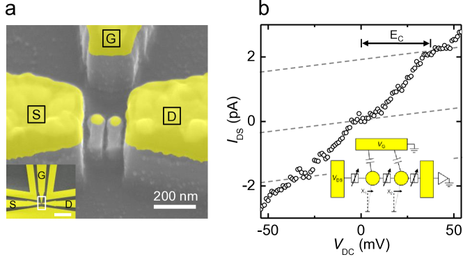
The two nanopillars are defined on a silicon-on-insulator (SOI) substrate, where the top crystalline silicon is nm thin and the insulating SiO2 is about nm. A nm top gold layer serves as the final electrical conduction path. The deposited metal is also employed as a mask in a dry etch step, which mills out the SOI material around the pillars. We apply a CF4 plasma etch step and mill into the SiO2 insulating layer, thus ensuring electron transport via the metallic islands. Further details on the processing are given by Kim et al. kim_apl07 . In Fig. 1(a), the final sample is shown in a scanning electron microscope graph. The source and drain contacts are placed in close proximity to the two pillars. The distance between the pillars is about 17 nm. The gating electrode is placed further away, enabling a shift in the electrostatic potential of the islands. The inset of Fig. 1(a) gives a broader view of the coplanar-waveguides into which the two nanopillars are embedded.
The nanoscale circuit is placed in an impedance matched transmission line in order to minimize signal loss along the line. All measurements are performed under vacuum ( mbar) in a probe station at room temperature. The station is placed in a Faraday cage and equipped with radio frequency contact probes covering the range from DC to 50 GHz (a bias-tee allows AC/DC superposition with high precision). The equivalent circuit diagram is given in the inset of Fig. 1(b): The two pillars are individually displaced by and , which lead to tunable resistances and mutual capacitances (arrow boxes). The gating electrode couples capacitively to the pillars. The output current of the coupled electron shuttles is fed into a current amplifier.
I Results and Discussion
The resulting -characteristic is shown in Fig. 1(b): the application of a DC bias voltage only across the coupled pendula leads to an ohmic response, modulated by Coulomb blockade steps. The gate electrode is grounded in these measurements. The total Coulomb energy marks the energy required to transport a single charge through an island alex . From the data in Fig. 1(b) (marked by the arrow) we find a total energy of meV. The capacitance of each island of radius can be estimated to be , where the inter-nanopillar distance is nm. In accordance with the optimized values that fit the experimental model (see Methods section), we obtain aF and aF, where we used for the islands’ radii the values nm and nm. Since the two islands are placed in series, the total capacitance is . Hence, we obtain a total capacitance of aF, from which we extract a Coulomb energy of meV. This is well above the corresponding room temperature energy of 26 meV. We stress that room temperature CB for a coupled shuttle has not been observed before. Conventional single electron shuttles reveal CB only at low temperature azuma ; azuma2 , since suppression of co-tunneling is not as pronounced as for the coupled shuttles considered in this work.
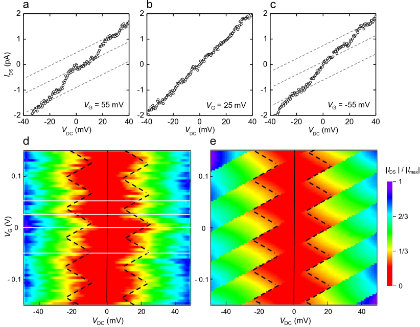
In Fig. 2 the response to a pure DC-bias and gate voltage of the coupled shuttles is studied. -curves at altered gate voltages are shown in Fig. 2(a–c). The dashed lines are linear extrapolations of the initial conductance slopes and underline the steps caused by single electron charging. Evidently, a typical Coulomb staircase is superimposed on an ohmic response, due to thermal broadening and shuttling gorelik . Note that the mechanical motion of the shuttles allow exchange of electrons with one electrode while suppressing it on other electrode. Since the applied gate voltage changes the potential around the shuttles, the charging energy required for an additional electron on the island can be varied accordingly. The trace at mV in Fig. 2(b) shows an ohmic response without the CB steps. As the gate voltage decreases, the Coulomb staircase reappears ( mV), as shown in Fig. 2(c). The traces are not symmetric about zero bias, which is due to the slightly different diameters of the nanopillar islands and the possible polarization of an oxide layer on the islands wilkins . The full DC output signal from a measurement run is summarized with respect to both and in Fig. 2(d), revealing Coulomb diamonds. We note that the diamond structure compares to that of a single island, due to the common and the similar size of the islands. The lack of symmetry of the diamonds with respect to = 0 is due to the actual difference in island radii, and to the difference in capacitance couplings to the source or drain. Although the obtained curves do not show clear steps due to the thermal environment, the periodic variation of the source-drain offset voltages is seen. The line plots for and mV are indicated by the white horizontal lines in Fig. 2(d). To validate the experimental results, we compute the current using numerical methods (see the Methods section). The theoretical results shown in Fig. 2(e) reproduces the shape and size of the measured Coulomb diamonds and agrees with the estimated size of the islands.
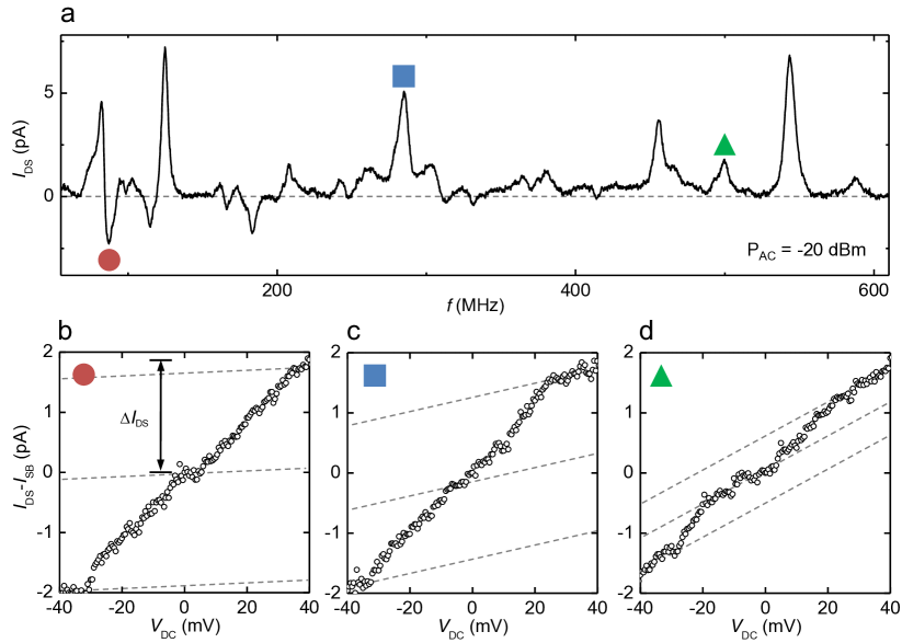
Next we apply an RF signal with zero DC bias in order to tune the mechanical motion of the system, as shown in Fig. 3(a). The ability to ‘dial in’ the shuttling frequency is the fundamentally new feature of this device, as compared to classical single electron transistors. We can now trace the DC bias voltages at the three different mechanical modes marked in Fig. 3(a), plotted in Fig. 3(b), (c) and (d), respectively. These correspond to commensurate mode numbers of the fundamental mode (for more details, see ckim_prl10 ): is 1/6 (circle, = 87MHz), 5/9 (square, = 289MHz) and 1/1 (triangle, = 500MHz). The current offset due to spontaneous symmetry breaking (SB) in coupled electron shuttles ckim_prl10 is subtracted. Dashed lines extend the inclined plateaus to underline the staircase current.
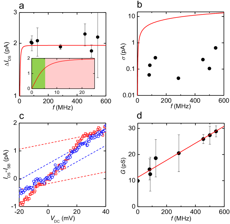
Fig. 4(a) exemplifies the dissipative regime: In this limit, a saturation current (frequency independent) is achieved, as the effective contact time of the islands with the electrodes is proportional to the inverse of the frequency, and at the same time, the current is proportional to the time contact and to the frequency (see Methods section). We observe a saturation value for the current of about 2 pA. The measured current steps (black dots) fall on the expected shuttle current (red solid line), as predicted from 2. We have to note that their calculation only considered a single shuttle. The inset in Fig. 4(a) shows a magnified view of the expected current in the low frequency region. The coupled shuttles are operated in the high frequency, dissipative limit (red region). We estimated 5-8 nm, 17 nm, and 1 nm, giving . We also have s. Thus, we find the transition frequency to be of the order of 5 MHz, which agrees very well with our data. The standard deviation of the experimental values are found to be much lower than the theoretically expected fluctuations, as seen in Fig. 4(b). This can be ascribed to the fact that the model assumed a single shuttle unlike the actual device of two coupled charge shuttles in series. However, charge fluctuations are even more strongly suppressed off by the mechanical resonances for two coupled shuttles.
We consider now the conductance level within the plateau. Fig. 4(c) shows two -traces at 285 MHz (red squares) and 500 MHz (blue circles). The dashed lines give the slopes of the corresponding plateaus in the neighboring Coulomb regions. The slope, or differential conductance , increases linearly towards higher shuttling frequencies, a consequence of self-excitation. This occurs around = 0, where a mechanical mode was located, and at . In the CB regime, the number of transferred electrons per period is quantized in units of , . Moreover, in the self-oscillatory regime (above a critical voltage, gorelik , or around , where the mechanical mode was excited), the charge exchange with the leads takes a fixed quantized value corresponding to the thermal equilibrium with the nearest lead, and is exponentially suppressed with the far lead. Following Gorelik et al. we estimate the critical voltage to be of the order of the CB voltage, gorelik . In this regime, the conventional linear-in-frequency relation applies, . Note that for intermediate values, 0 , the amplitude of the self-oscillations is suppressed. In this region, 2 applies, rather than the linear-in-frequency relation (see also the Methods section). The overall results are summarized in Fig. 4(d), where we show the step differential conductance in the plateau, , or the slope of the dashed lines of Fig. 4(c). The linearity in frequency of the plateau differential conductance is evident. This demonstrates the self-excitation of the nanopillars, already shown to cause ohmic behavior kim_njp10 ; zettl_nl10 .
II Conclusion
In summary we observe Coulomb blockade in a coupled electron shuttle operating at room temperature. Mechanical clocking of electron transport has been demonstrated by using RF signals. Operating in the high frequency regime leads to a strong suppression of current fluctuations. Two regimes of operation are observed in the high frequency limit as a function of bias voltage, corroborating theoretical predictions: the dissipative regime, where the current is frequency independent, and the self oscillatory CB regime, showing a linear-in-frequency conductance.
III Methods
To validate the experimental results obtained in Fig. 2(a-d), we compute the current within the orthodox model of CB. The accessible states are described by their respective probabilities , where is the number of excess electrons on the islands . In the absence of an RF signal, the system can be assumed to be in the dissipative regime, where the amplitude of the mechanical oscillations is small and the tunneling current prevails over the shuttle current gorelik . Changes in the resistance of a particular junction are proportional to , with being the typical tunneling distance, the displacement, and in the dissipative regime. In this limit, we suppose 1/ to be much smaller than the typical time scale of the displacements, and the time evolution can be described in terms of coupled master equations ahn , which we solve by exact diagonalization. In the CB limit, we observe that , where denotes an ensemble average. gives the rate of tunneling from left to right at one of the junctions for a given configuration :
| (1) |
with being the average resistance of the junction and the chemical potential. The theoretical results are shown in Fig. 2(e): the CB region below the first transition is shown in red. We stress that a finite conductance is observed in this region due to thermal broadening and direct electron shuttling. In the dissipative regime, however, we assume temperature broadening to be the dominant source of the ohmic response.
We now focus on the ohmic response between the differential conductance plateau or current step, . Conventionally, one would expect a simple linear relation between this ohmic current and the shuttling frequency of the form, or , which is typically applied for electrometry purposes nato_asi . This relation, however, is only valid in the limit of large tunneling rates, with defined in 1. For our setup, the relation applies only in the self-oscillatory regime, achieved in the plateau or around , where a mechanical mode is excited. Our theoretical results indicate that in the inter-plateau region 5-15 MHz, which is slower than the mechanical motion. Hence, we can state that the coupled shuttles operates in the dissipative regime. According to Weiss & Zwerger weiss_zwerger , we can calculate in this regime the average number of transferred electrons per period:
| (2) |
where , and 2 is the effective contact time, . The length indicates the maximum displacement of the mechanical oscillation, and . In the regime of high RF frequencies, the effective contact time is shorter than the charge relaxation time, . Thus the number of transferred electrons per period is inversely proportional to the frequency of the shuttle oscillation, with . Then, the electron shuttle current achieves a frequency independent saturation value, .
Acknowledgements We are grateful to G. Platero for enlightening discussions. The authors like to thank DARPA for support through the NEMS-CMOS program (N66001-07-1-2046), the University of Wisconsin-Madison for support with a Draper-TIF award and the Spanish Ministry of Education, program (SB2009-0071).
References
- (1) M. I. Tinkham, Introduction to Superconductivity (McGraw-Hill, New York, 1996).
- (2) L. Leuzzi, C. Conti, V. Folli, L. Angelani, and G. Ruocco, Phase Diagram and Complexity of Mode-Locked Lasers: From Order to Disorder, Phys. Rev. Lett. 2009, 102, 083901-083905.
- (3) Chang, P. ; Yamagata, T. ; Schopf, P. ; Behera, S. K. ; Carton, J. ; Kessler, W. S. ; Meyers, G. ; Qu, T. ; Schott, F. ; Shetye, S.; Xie, S. – P. et al., Climate Fluctuations of Tropical Coupled Systems – The Role of Ocean Dynamics, J. Climate 2006, 19, 5122-5174.
- (4) K. H. Han, and D. E. Postnov, Chaotic Bursting as Chaotic Itinerancy in Coupled Neural Oscillators, Chaos 2003, 13, 1105-1110.
- (5) Blick, R. H. ; Erbe, A.; Pescini, L.; Kraus. A.; Scheible, D. V.; Beil, F. W.; Hoehberger, E.; Hoerner, A.; Kirschbaum, J.; Lorenz, H.; et al.,Nanostructured Silicon for Studying Fundamental Aspects of Nanomechanics, J. Phys. Cond. Matt. 2002, 14, R905-R945.
- (6) Blencowe, M., Nanomechanical Quantum Limits, Science 2004, 304, 56-57.
- (7) Roukes, M. L., Nanoelectromechanical Systems Face the Future, Phys. World 2001, 14, 25-32.
- (8) Craighead, H. G., Nanoelectromechanical Systems, Science 2000, 290, 1532-1535.
- (9) Cleland, A. N. Foundations of Nanomechanics, Springer, 2002.
- (10) Erbe, A.; Weiss, C.; Zwerger, W.; Blick, R. H., Nanomechanical Resonator Shuttling Single Electrons at Radio Frequencies, Phys. Rev. Lett 2001, 87, 096106-096109.
- (11) Scheible, D. V.; Weiss, C.; Kotthaus, J. P.; Blick, R. H., Periodic Field Emission from an Isolated Nanoscale Electron Island, Phys. Rev. Lett. 2004, 93, 186801-186804.
- (12) Koenig, D.; Weig, E. M.; Kotthaus, J. P., Ultrasonically Driven Nanomechanical Single-Electron Shuttle, Nature Nanotech. 2008, 3, 482-489.
- (13) Scheible, D. V.; Blick, R. H., Silicon Nanopillars for Mechanical Single-Electron Transport, Appl. Phys. Lett. 2004, 84, 4632-4634.
- (14) Kim, H. S.; Qin, H.; Blick, R. H., Direct Mechanical Mixing in a Nanoelectromechanical Diode, Appl. Phys. Lett. 2007, 91, 143101-143103.
- (15) Kim, H. S.; Qin, H.; Blick, R. H., Self-Excitation of Single Nanomechanical Pillars, New J. Phys. 2010, 12, 033008-033010.
- (16) Gorelik, L. Y.; Isacsson, A.; Voinova, M. V.; Kasemo, B.; Shekhter, R. I.; Jonson, M. Shuttle Mechanism for Charge Transfer in Coulomb Blockade Nanostructures, Phys. Rev. Lett. 1998, 80, 4526-4529.
- (17) Shekhter, R. I.; Gorelik, L. Y.; Jonson, M.; Galperin, Y. M.; Vinokur, V. M. Nanomechanical Shuttle Transfer of Electrons, J. Comput. Theor. Nanosci. 2007, 4, 860-895.
- (18) Weiss, C.; Zwerger, W. Accuracy of a Mechanical Single-Electron Shuttle, Europhys. Lett. 1991, 47, 97-103.
- (19) Geerligs, L. J.; Anderegg, V. F.; Holweg, P. A. M.; Mooij, J. E. Frequency-Locked Turnstile Device for Single Electrons, Phys. Rev. Lett. 1990, 64, 2691-2694.
- (20) Kim, C.; Park, J.; Blick, R. H. Spontaneous Symmetry Breaking in Two Coupled Nanomechanical Electron Shuttles, Phys. Rev. Lett. 2010, 105, 067204-067207.
- (21) Holleitner, A. W.; Blick, R. H.; Hüttel, A. K. H.; Eberl, K.; Kotthaus, J. P.; Probing and Controlling the Bonds of an Artificial Molecule, Science 2002, 297, 70-72.
- (22) Azuma. Y.; Hatanaka, T.; Kanehara, M.; Teranishi, T.; Chorley, S.; Prance, J.; Smith, C. G.; Majima. Y., One by one Single-Electron Transport in Nanomechanical Coulomb Blockade Shuttle, Appl. Phys. Lett. 2007, 91, 053120-053122.
- (23) Azuma, Y.; Kanehara, M.; Teranishi, T.; Majima, Y. Single Electron on a Nanodot in a Double-Barrier Tunneling Structure Observed by Noncontact Atomic-Force Spectroscopy, Phys. Rev. Lett. 2006, 96 016108-016111.
- (24) Wilkins, R.; Ben-Jacob, E.; Jaklevic, R. C. Scanning-Tunneling-Microscope Observations of Coulomb Blockade and Oxide Polarization in Small Metal Droplets, Phys. Rev. Lett. 1989, 63, 801-803.
- (25) Ahn, K-H.; Park, H. C.; Wiersig, J.; Hong, J. Current Rectification by Spontaneous Symmetry Breaking in Coupled Nanomechanical Shuttles, Phys. Rev. Lett. 2006, 97 216804-216807.
- (26) Grabert, H.; Devoret, M. H. Single Charge Tunneling: Coulomb Blockade Phenomena in Nanostructures, Plenum: New York, 1992.
- (27) Weldon, J. A.; Alemn, B.; Sussman, A.; Gannett, W.; Zettl, A. K. Sustained Mechanical Self-Oscillations in Carbon Nanotubes, Nano Lett. 2010, 10, 1728-1733 .