Self-trapping nature of Tl nanoclusters on Si(111)-77 surface
Abstract
We have investigated electronic and structural properties of thallium (Tl) nanoclusters formed on the Si(111)-77 surface at room temperature (RT) by utilizing photoemission spectroscopy (PES) and high-resolution electron-energy-loss spectroscopy (HREELS) combined with first principles calculations. Our PES data show that the state S2 stemming from Si restatoms remains quite inert with Tl coverage while S1 from Si adatoms gradually changes, in sharp contrast with the rapidly decaying states of Na or Li nanoclusters. No Tl-induced surface state is observed until =0.21 ML where Tl nanoclusters completely cover the faulted half unit cells (FHUCs) of the surface. These spectral behaviors of surface states and a unique loss peak L2 associated with Tl in HREELS spectra indicate no strong Si-Tl bonding and are well understood in terms of gradual filling of Si dangling bonds with increasing . Our calculational results further reveal that there are several metastable atomic structures for Tl nanoclusters at RT transforming from each other faster than 1010 flippings per second. We thus conclude that the highly mobile Tl atoms form self-trapped nanoclusters within FHUC at RT with several metastable phases. The mobile and multi-phased nature of Tl nanoclusters not only account for all the existing experimental observations including the fuzzy scanning tunneling microscope images and a dynamical model proposed by recent x-ray study but also provides an example of self-trapping of atoms in a nanometer-scale region.
I INTRODUCTION
Since the success of atom-trapping in microwave cavity using the field from a single photon,Haroche efforts have been continued to cool-down atoms with a better spatial resolution motivated by numerous applications including Bose-Einstein condensates, high-precision atomic clocks, and scalable quantum computers.Vul ; Hood Despite such elaborate research endeavor, the confinement of a single atom has been limited only to a few tens of micrometer. We, however, report that nature allows the trapping of several thallium (Tl) atoms into a region of nanometer scale in the form of a nanocluster on the Si(111)-77 surface at room temperature (RT). The trapping of Tl atoms appears to be distinctly different from typical features of TlSi atomic bonding revealing a remarkably mobile character of Tl nanoclusters and significant inertness on substrate surface electronic states.
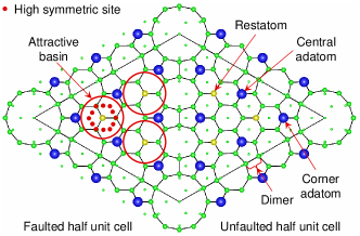
Because of its unique atomic arrangement of the unit cell consisting of a faulted half unit cell (FHUC) and an unfaulted half unit cell (UFHC) as depicted in Fig. 1, the Si(111)-77 surface has been used as a fascinating template to fabricate a crystalline array of self-assembled nanoclusters of various atomic species. Most adsorbates upon forming nanoclusters are found to occupy high symmetric sites around Si restatoms known as attractive basins (red circles in Fig. 1).CK Those nanoclusters formed on this surface at RT exhibit atomically well-resolved scanning tunneling microscopy (STM) images with six atoms in one or both half unit cells and appear to be semiconducting.Li ; Wu ; Li2 Tl nanoclusters, however, has been known to be exceptional to this trend showing fuzzy STM images and reported to be metallic.Vitali It has been proposed that each Tl nanocluster contains nine mobile Tl atoms, instead of six as for most other nanoclusters, formed only in FHUC to account for such distinct features of Tl nanoclusters.Vitali ; Zotov Moreover studies on electronic band structures of most nanoclusters other than Tl suggest a strong chemical bonding between adsorbates and Si atoms accompanying significant displacement of central Si atoms by adsorbates.Zhang ; Ahn ; Wei Such a strong chemical bonding may explain why the STM images of nanoclustares are so well resolved atomically for those nanoclusters except Tl nanoclusters.
Motivated by such peculiar features of Tl nanoclusters, we have investigated electronic and structural properties of Tl nanoclusters formed on the Si(111)-77 surface by utilizing photoemission spectroscopy (PES) and high resolution electron energy loss spectroscopy (HREELS). We also have carried out first principle total energy calculation to estimate thermal stability of atomic arrangement of Tl nanoclusters at RT. We find that the substrate surface states, especially associated with Si restatoms, are quite inert to Tl adsorption until the completion of formation of nanoclusters in contrast to nanoclusters of other atomic species. Such a remarkable inertness of surface states together with invisible semiconducting band gap in HREELS spectra suggest a distinctly weak chemical bonding between Tl and Si atoms. This also may eliminate a possibility of displacing Si center adatom by Tl, which is often observed for most other nanoclusters formed on Si(111)-77 surface. Our results of first principle total energy calculation for several plausible atomic models of Tl nanoclusters, in fact, support such a scenario by revealing relatively small energy differences between different atomic models, and thus a significant hopping rate between different atomic configurations within the same attractive basin at RT. We find a ”dynamic trapping state” of Tl nanoclusters in a sense that a single Tl nanocluster consisting of nine Tl atoms is rapidly changing its atomic configuration due to the low diffusion barriers between neighboring high symmetry sites in the attractive basin while residing only in a FHUC. We present experimental evidence and discuss physical implication of the dynamic trapping state.
II EXPERIMENTAL DETAILS
The PES chamber used to measure the valence band of our sample has a high intensity He I discharge lamp (Omicron HIS-13 ) and a SPECS Phoibos-100 electron analyzer with an optimal resolution of 110 meV at RT. The HREELS system utilizes a Leybold-Heraeus ELS-22 spectrometer with an optimum resolution of 19 meV. Both the PES and the HREELS chambers equipped with several surface diagnostic probes including low energy electron diffraction (LEED) have been maintained with a base pressure of less than 110-10 Torr during the entire course of measurements. We have prepared our sample by using a high-doped n-type Si(111) wafer with a resistivity of 2 cm. A Tl source was made by wrapping a small piece of Tl with a tungsten wire. We have thoroughly degassed sample and Tl source with the chamber pressure controlled under 310 Torr for several hours. The clean Si(111)-77 phase was obtained after cleaning the sample with a well known recipe, i.e., heating up to 1200 ∘C for 10 seconds followed by annealing at 800 ∘C for about 5 minutes. The cleaned sample showing a well defined 77 LEED pattern was then cooled to RT before depositing Tl. We have first monitored intensity variation of fractional-order LEED spots during the continuous deposition of Tl atoms onto the clean Si(111)-77 surface at RT. The seventh order LEED spots becomes sharper and stronger as Tl coverage increases and reaches a maximum in intensity at =0.2 monolayers (MLs) due to the constructive interference from a lattice-like array of Tl nanlclusters. For 0.2 ML, the spots become weaker and fuzzier with increasing coverage indicating an increasing disorder due to the extra Tl atoms added on the Tl nanoclusters.Hwang Thus the completion of formation of a crystalline array of Tl nanoclusters on the Si(111)-77 surface were relatively easily detected by the local maximum in intensity of the (1/7 0) LEED spot at =0.2 ML in agreement with previous STM study.Vitali
III RESULT AND DISCUSSION
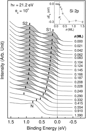
In Figure 2, we present a progressive spectral change of the valence band of the Si(111)-77 surface at RT with increasing . The spectra were measured at an emission angle of 10∘ from the surface normal. One notes the well-defined surface states S1 and S2 from the clean Si(111)-77 surface at binding energies of 0.15 and 0.87 eV below the Fermi level. These states has been associated with central Si adatoms and Si restatoms, respectively.Uhr The contribution from corner Si adatoms has been reported to appear with binding energy of 0.5 eV.Uhr This contribution apparently is not well resolved at RT and causes the line shape of S1 asymmetric. The binding energy of the spectra in Fig. 2 has been corrected by taking the band bending effect into account from the Si 2 core-level shift as a function of (see inset). We find that the bulk component of the Si 2 core-level remains unaffected by Tl adsorption until =0.2 ML where the array of Tl nanoclusters is best developed, and then begins to change rapidly with exhibiting a band bending effect due to the different chemical morphology from that of Tl nanoclusters.
We notice in Fig. 2 that the two surface states are not significantly affected by the Tl adsorption at initial stage for 0.21 ML. This is especially true for S2, which is in sharp contrast with adsorption of other metal atoms, Li and Na for example, where S2 disappears almost completely at a Na coverage as small as 0.03 ML.Ahn ; Wei We also note that no new state associated with Tl appears until =0.91 ML where a new state N begins to show up. We remind that a new state appears for the Na adsorption as early as at 0.03 ML.Ahn ; Wei It is interesting to find, however, that adsorption of K shows the spectral change with K coverage quite similar to the one caused by Tl.K05 In order to examine the spectral changes more quantitatively, we have fitted the spectra with Gaussian peaks after subtracting the background with a polynomial function in the form of .
We present our fit-results in Fig. 3 for the states S2 in (a) and S1 in (b). Both states reveal remarkable spectral changes as coverage crosses =0.2 ML as also seen from the structural changes in previous STM study.Vitali While the binding energy and the intensity of S2 changes gradually up to , they change more significantly for . Such a trend seems to be reversed for S1. More specifically while the binding energy of S2 (S1) is increased by 20 (90) meV at , intensity of S2 (S1) is decreased by 14 (50) %.
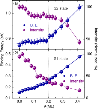
Now we think of several plausible mechanisms to explain such spectral changes in Fig. 3. One may first consider the filling of the half-filled Si dangling bonds by the charge transfer from Tl atoms. Here we assume no displacement of central Si adatoms by Tl since there is no new surface state appearing at least until =0.2 ML. The half-filled S1 state pinning the Fermi level at 0.63 eV above from valence band maximumHimp becomes increasingly filled by the electrons from Tl atoms so as to make the state shift towards the higher binding energy side as observed in Fig. 3. Similar shifts have been reported also for the electron doped bulk crystal or K adsorbed graphene.King ; Ohta The decreased intensity of S1 by 50 % suggests the filling of the dangling bonds of central Si adatoms only in FHUC, which is consistent with earlier STM observation of Tl nanoclusters formed only in FHUC.Vitali While S1 is affected significantly by the filling, S2 state may remain inert as observed when the charge transfer is limited mainly to the central Si adatoms.
Another possibility to explain binding energy shifts of the surface states, especially for the remarkable binding energy shift of S1 state, is the effect driven by the enhanced inter-clusters interaction due to the reduced separation between neighboring nanoclusters with increasing . El-Moghraby et. al, showed in their calculation that the reduced inter-clusters separation results in lowering the ground level energy due to the enhanced inter-clusters interaction.Mogh Similar trend has been reported also for the excitonic energies of quantum dots.Zunger Since exciton is associated with electron-hole pair excitations, the enhanced excitonic energy indicates the shift of valence band so that the binding energy shift of the surface state S1 may be caused partly by the enhanced inter-clusters interaction with increasing . Unfortunately we can not quantify the amounts of shifts due to this interaction at present since no relevant calculations available. We reported that the constant work function change observed during the coverage range while the Tl nanoclusters were formed might be understood by the enhanced inter-clusters interaction.Hwang Although one may still think of a possibility that a new surface state may exist quite near to the S1 and/or S2 states but is hidden because of its weak intensity. Since the line-widths of both surface states remain almost unchanged with up to 0.21 ML, however, we ruled out this possibility. The only visible new state associated with Tl adsorption appears for 0.91 ML as shown in Fig. 2.
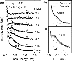
Our HREELS data presented in Fig. 4 shows the spectral change with Tl adsorption. we have fitted the HREELS spectra for a quantitative analysis as done earlier.Lait ; Ahn00 The spectral behavior turns out to be quite consistent with the explanation of our PES data based on the filling of dangling bonds of central Si adadtoms. One first notices a Drude tail indicating the metallic nature of the clean Si(111)-77 surface. In Fig. 4 (b), we also find a loss peak L1 of loss energy E=0.30 eV observed only at off specular angle. Since the relatively broad line-width (187 meV) of L1 and small electron concentration of a Tl nanocluster, we safely rule out possibilities of a local vibrational origin and a plasmon. It certainly can not be a phonon since the energy is higher than the highest optical phonon energy (57 meV) and no multiple phonon peaks are observed. We thus attribute L1 to an interband transition between states below and above the Fermi-level of the Si(111)-77 surface.
The interesting feature we emphasize in Fig. 4 is the presence of a loss peak L2, which shifts toward the higher loss energy while concomitantly losing its intensity. It disappears completely as shown by the featureless spectrum at =0.5 ML when Tl nanoclusters no longer maintain their unique atomic arrangement due to the extra Tl atoms. Such spectral behavior of L2 may be easily understood considering the filling of dangling bonds of Si adatoms as for the binding energy shift of S1 state in our PES spectra in Fig. 2. As the dangling bonds in FHUC are gradually filled by the charge donation from Tl atoms with increasing , the spectral intensity or density of states (DOS) decreases accordingly in the vicinity of Fermi level. Therefore the metallicity of the surface becomes gradually deteriorated by losing its dangling bonds due to Tl adsorption. Since the gradual loss of the metallicity causes the weight center of the S1 state to shift towards the higher binding side as shown in Fig. 3, such a change in DOS near Fermi level should show up as a loss peak L2 shifting towards the higher loss energy with diminishing intensity as increases. For , the DOS at the Fermi level becomes a noise level with S1 significantly quenched, which is consistent with the HREELS spectrum at =0.5 ML where L2 disappeared completely. Since the Tl nanoclusters are formed only in FHUC, the surface does not show a band gap due to the remaining dangling bonds in UHUC even though it is completely covered with Tl nanoclusters in FHUC at 0.20 ML.
In order to confirm our explanation for the experimental observations discussed above, we have carried out first principles density-function calculations using ab initio plane wave pseudo-potential method (VASP code) in conjunction with projector augmented wave potentials within the generalized-gradient approximations (GGA).vasp ; gga The calculation employs a plane wave basis set with an energy cutoff of 250 eV for single point in the Brillouin zone. The unit cell in slab model consists of 19 Tl and 12 Si adatoms in addition to 6 layers of Si and 49 H atoms passivating Si dangling bonds in the bottom layer.
As a first step to find the most stable atomic structure of a Tl nanocluster, we have calculated adsorption energy for several high symmetry sites in the attractive basin (see inset in Fig. 5). Details of calculational results will appear elsewhere.Lee07 The bridge site in a FHUC is found to be the most stable with an adsorption energy = 2.36 eV/atom favoring over the same site in UHUC of = 2.30 eV/atom. When the second (third) Tl atom is placed at another bridge site around a neighboring restatom, is decreased by 0.008 (0.01) eV/atom indicating attractive interaction between Tl atoms within FHUC. Therefore a nanoclusdter begins to form only in FHUCs by this attractive interaction between Tl atoms as observed in STM study.Vitali On the other hand when three atoms of Al (Ga) are adsorbed at on-top sites () on Si atoms in the second layer, the most favored for a single Al (Ga) atom adsorption, is increased by 0.14 (0.01) eV/atom.Lee-cpc Because of the repulsive interaction between the first two Al (Ga) atoms, Al (Ga) nanoclusters are formed in both half unit cells as observed also in the previous STM studies.Jia ; Chang
Although the STM image of the surface with Tl nanoclusters best developed at 0.2 ML appears fuzzy, Pb nanoclusters having about similar atomic mass or In nanoclusters belonging to the same elemental group exhibit atomically well resolved STM images. One may notice that the Pb and In nanoclusters are formed with central Si adatoms significantly displaced by adsorbate atoms.Li2 ; Li For Tl nanoclusters no evidence of such a substrate reconstruction is found in PES or in HREELS data since no new surface state induced by Tl is seen in PES spectra or any loss peak associated with Tl indicating a strong chemical bonding has been observed. Zotov et. al., reported, however, that the Tl adsorbed surface revealed several stable atomic structures depending on when annealed at a mild temperature, which showed well resolved STM images. Therefore the surface with Tl nanoclusters at RT is a metastable surface where Tl nanoclusters are thought to be quite mobile to produce such fuzzy STM images.Vitali Such a mobile nature of Tl nanoclusters has also been suggested by our earlier x-ray study thus proposing a dynamical model where four different atomic configurations of Tl nanoclusters coexist at RT.Kim
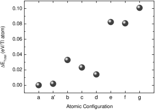
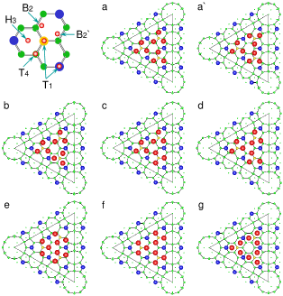
With this background, we have calculated the hopping rate of Tl atoms to estimate the mobility at RT for eight different atomic structures depicted in Fig. 5. Possible structures other than those eight models are ruled out since occupation of bridge sites is favored over other high symmetry sites, for example, the on-top or hollow sites () by 0.07 and 0.10 eV/atom, respectively. We assumed no reconstruction of substrate surface or replacement of Si atom with adsorbetes and each Tl nanocluster contains nine Tl atoms as indicated by the coverage of 0.2 ML, 9 Tl atoms on 49 Si atoms, for the fully developed Tl nanoclusters in FHUCs. The total energy difference calculated for the eight structures is presented in Fig. 6. One finds that the differences among the structures are less than 0.10 eV/atom. The small total energy difference among eight possible structures strongly suggests a dynamical model proposed by x-ray study.Kim
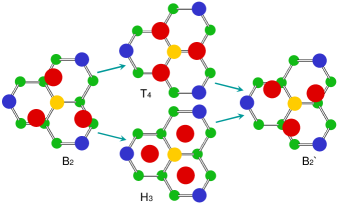
In order to estimate the hopping rate of Tl atoms between high symmetry sites, we assumed the half unit cell of Si(111)-77 surface as a potential well with a lateral length of 26.8 Å considering the Si dimers as the boundary of the well. This assumption is based on the fact that the Si dimers constituting the boundary of the unit cell is found to be the most unstable adsorption sites for metal atoms.CK
As an example of hopping process, we have considered two processes shown in Fig. 7 where the stable Tl atoms occupying B2 sites initially move to anther stable sites B2’ by overcoming the energy barriers Ed=0.07 eV at T4 sites and Ed=0.10 eV at H3 sites. To calculate the hopping rate , we adopted the equation , where is attempt frequency, is energy barrier, is Boltzmann constant, and is sample temperature. The attempt frequency defined as a colliding frequency of atoms to the energy barrier has been evaluated for Pb, Y, and Ag atoms within the half unit cell as 5109 hoppings/s.Vasco In the calculation by Vasco et. al., they assumed no hoppings between attractive basins for the convenience of calculation. We note that this value of on the Si(111)-77 surface is smaller than typical values on metal surfaces of 10111013 hoppings/s.Vasco Since depends on the width of a potential well , we have used =71011 hoppings/s because of the reduced width =2.2 Å between the two bridge sites within a single attractive basin with barriers at or sites. We thus obtain =41010 hoppings/s for the upper path in Fig. 7 and 11010 hopping/s for the lower path at RT. Such significant values of the hopping rate of Tl atoms clearly indicate that the Tl nanoclusters are quite mobile at RT. Their hopping, however, is restricted within the same attractive basin of the FHUC because of much higher energy barriers between the basins and between the neighboring FHUCs.CK ; Wu Considering the average scanning frequency of 0.25 scans/s for STM measurement of a half unit cell,Polop the fuzzy STM images of Tl nanoclusters can be caused by such high hopping rates between several metastable atomic configurations as suggested also by recent x-ray study.Kim We thus confirm that Tl nanoclusters formed on the Si(111)-77 surface are quite mobile to rapidly transform their atomic configurations at RT and show no strong bonding between Tl and substrate Si atoms. The Tl nanoclusters, therefore, provides an example of self-trapping a nanocluster in nature within a region as small as nanometer scale.
In addition to such a high mobility, the attractive interaction of a FHUC occupying Tl atom for an additional Tl atom result between Tl atoms within an
IV SUMMARY
We have measured electronic properties of the crystalline array of Tl nanoclusters formed on Si(111)-77 surface at RT. The valence band PES data show no Tl-induced surface state while intrinsic Si surface states S1 and S2 remain relatively inert until the Tl coverage of 0.21 ML where Tl nanoclusters cover the entire FHUCs of the surface. Such a behavior of Si surface states is in sharp contrast with nanoclusters of other atomic species such as Na or Li nanoclusters where they are rapidly quenched at an early stage of adsorption. No band gap is observed and a characteristic loss peak associated with Tl adsorption in HREELS data shifts towards the higher loss energy side with gradual decreasing spectral intensity as Tl nanoclusters are formed. All these experimental data are understood in terms of the filling of dangling bonds stemming from Si adatoms. Inter-clusters interaction also seems to play a role in driving the additional shift of S1 state. Our theoretical calculation is found to support our explanation based on the filling of dangling bonds and further suggests that the Tl nanoclusters are quite mobile to transform their atomic arrangements by hopping through rather shallow energy barriers between high symmetry binding sites with a rate faster than 1010 hopping/s at RT. We thus conclude that Tl atoms form nanoclusters self-trapped in FHUCs and highly mobile within the FHUCs with several different structural phases at RT. These unique features of Tl nanoclusters and the absence of strong TlSi bondings account for all the experimental data not only discussed here but also other available observations such as the puzzling fuzzy STM images and a dynamical mixing model proposed by x-ray study. The system of Tl nanoclusters self-trapped in potential wells of nanometer scale i.e., within the FHUCs of the Si(111)-77 surface, at RT may thus be a good candidate to study Rabi oscillation for numbers of quantum dot arrays or to explore the possibility as quantum qubits for highly dense optical devices.XLi
This work was supported by the Korea Research Foundation Grant funded by the Korean Government (MOEHRD, Basic Research Promotion Fund (KRF-2006-312-C00513). J. S. Kim acknowledges the support from KISTI (Korea Institute of Science and Technology Information) under [The Strategic Supercomputing Support Program].
References
- (1) S. Haroche, M. Brune, and J.M. Raimond, Europhys. Lett. 14, 19 (1991).
- (2) V. Vuletić and S. Chu, Phys. Rev. Lett. 84, 3787 (2000).
- (3) C.J. Hood, T.W. Lynn, A.C. Doherty, A.S. Parkins, and H.J. Kimble, Science 287, 1447 (2000).
- (4) K. Cho and E. Kaxiras, Surf. Sci. 396, L261 (1998).
- (5) J.-L. Li et al., Phys. Rev. Lett. 88, 066101 (2002).
- (6) S.-C. Li, J.-F. Jia, R.-F. Dou, Q.-K. Xue, I.G. Batyrev, and S.B. Zhang, Phys. Rev. Lett. 93, 116103 (2004).
- (7) K. Wu et al., Phys. Rev. Lett. 91, 126101 (2003).
- (8) L. Vitali, M.G. Ramsey, and F.P. Netzer, Phys. Rev. Lett. 83, 316 (1999).
- (9) A.V. Zotov, A.A. Saranin, V.G. Kotlyar, O.A. Utas, and Y.L. Wang, Surf. Sci. 600, 1936 (2006).
- (10) L. Zhang, S.B. Zhang, Q.-K. Xue, J.-F. Jia, and E.G. Wang, Phys. Rev. B 72, 033315 (2005).
- (11) J.R. Ahn, K. Yoo, J.T. Seo, J.H. Byun, and H.W. Yeom, Phys. Rev. B 72, 113309 (2005).
- (12) C. Weindel, H.J. Jänsch, G. Kirchner, H. Kleine, J.J. Paggel, J. Roth, H. Winnefeld, and D. Fick, Phys. Rev. B 71, 115318 (2005).
- (13) C.G. Hwang, N.D. Kim, G. Lee, S.Y. Shin, S.H. Uhm, H.S. Kim, J.S. Kim, and J.W. Chung, Appl. Phys. A 89, 431 (2007).
- (14) R.I.G. Uhrberg, T. Kaurila, and Y.-C. Chao, Phys. Rev. B 58, R1730 (1998).
- (15) Kehui Wu, Y. Fujikawa, T. Briere, V. Kumar, Y. Kawaxoe and T. Sakurai, Ultramicroscopy 105, 32 (2005).
- (16) F.J. Himpsel, G. Hollinger, and R.A. Pollak, Phys. Rev. B 28, 7014 (1983).
- (17) D.M King et al., Phys. Rev. Lett. 70, 3159 (1993).
- (18) T. Ohta, A. Bostwick, T. Seyller, K. Horn, and E. Rotenberg, Science 313, 951 (2006).
- (19) D. El-Moghraby, R.G. Johnson, and P. Harrison, Comput. Phys. Commun. 155, 236 (2003).
- (20) G.A. Narvaez, L. He, G. Bester, A. Zunger, Physica E 32, 93 (2006).
- (21) P. Laitenberger and R.E. Palmer, Phys. Rev. Lett. 76, 1952 (1996).
- (22) J. R. Ahn, S. S. Lee, N. D. Kim, J. H. Min, C. G. Hwang, and J.W. Chung, Phys. Rev. Lett. 84, 1748 (2000).
- (23) G. Kresse and J. Hafner, Phys. Rev. B 47, 558 (1993); ibid. 54, 11169 (1996); 59, 1758 (1999).
- (24) J.P. Perdew and Y. Wang, Phys. Rev. B 45, 13244 (1992).
- (25) Geunsik Lee, Choon Gyu Hwang, Nam Dong Kim, Jinwook Chung, Sik Lee, and Jai Sam Kim, (unpublished)
- (26) Geunsik Lee, Jai Sam Kim, Comp. Phys. Commun., 177, 44 (2007)
- (27) H.H. Chang, M.Y. Lai, J.H. Wei, C.M. Wei, and Y.L. Wang, Phys. Rev. Lett. 92, 066103 (2004).
- (28) J. Jia, J.-Z. Wang, X. Liu, Q.-K. Xue, Z.-Q. Li, Y. Kawazoe, and S.B. Zhang, Appl. Phys. Lett. 80, 3186 (2002).
- (29) N.D. Kim, C.G. Hwang, J.W. Chung, Y.S. Kim, T.C. Kim, D.Y. Noh, H. Tajiri, K. Sumitani, and O. Sakata, (unpublished)
- (30) E. Vasco, C. Polop, and E. Rodriguez-Cañas, Phys. Rev. B 67, 235412 (2003).
- (31) C. Polop, E. Vasco, J.A. Martín-Gago, and J.L. Sacedón, Phys. Rev. B 66, 085324 (2002).
- (32) X. Li, Y. Wu, D. Steel, D. Gammon, T.H. Stievater, D.S. Latzer, D. Park, C. Piermarocchi, and L.J. Sham, Science 301, 809 (2003).