Capacitance of Graphene Bilayer as a Which-Layer Probe
Abstract
The unique capabilities of capacitance measurements in bilayer graphene enable probing of layer-specific properties that are normally out of reach in transport measurements. Furthermore, capacitance measurements in the top-gate and penetration field geometries are sensitive to different physical quantities: the penetration field capacitance probes the two layers equally, whereas the top gate capacitance preferentially samples the near layer, resulting in the “near-layer capacitance enhancement” effect observed in recent top-gate capacitance measurements. We present a detailed theoretical description of this effect and show that capacitance can be used to determine the equilibrium layer polarization, a potentially useful tool in the study of broken symmetry states in graphene.
I Introduction
Capacitance measurements probe the energy cost of moving charge between different parts of a system. In a classical system, this energy cost is a purely geometric quantity and consists of the electrostatic energy. In contrast, capacitance measurements performed on quantum systems can access a range of subtle and interesting phenomena. In particular, Pauli exclusion in degenerate electronic systems gives rise to a characteristic quantum contribution to the internal energy. The associated contribution to capacitance, known as ‘quantum capacitance’ Luryi1988 , is proportional to the electronic compressibility . In addition, at low carrier densities, the internal energy is dominated by electronic correlations, resulting in a so-called negative compressibility contribution to capacitance Bello1981 . In low dimensional systems these effects can amount to a sizeable contribution, making capacitance measurements a powerful probe of many-body effects Eisenstein1992 . Moreover, whereas electrical transport is often dominated by a small subset of electronic states, capacitance probes all states equally. Consequently, capacitance is a useful tool in the study of phenomena in which localization plays a role, such as quantum Hall effects and the metal-insulator transition Eisenstein1992 ; Eisenstein1994 ; Ilani2006 ; Dultz2000 ; Ilani2001 . Under certain conditions, the quantum capacitance can become an order-one effect Skinner2010 ; Li2010a .
Graphene and its bilayer are ideal materials for the application of the capacitance technique. The two-dimensional geometry of these materials permits the placement of proximal metal gates Ponomarenko2010 ; Henriksen2010 ; Young2010 , electrolytic solutionsXia2009 , or scanning probe heads Martin2008 ; Martin2009 , all of which can be used to probe capacitance. Interesting results have been obtained for monolayer graphene, in which this quantum capacitance was found to dominate the total capacitance near the Dirac point even at room temperature Xia2009 . Surprisingly, the compressibility measured at low temperature Martin2008 was found to be well described by the noninteracting massless Dirac model, a fact attributed to an exact cancelation of correlation effects in the monolayerAbergel2009 . In bilayer graphene (BLG), in contrast, the interaction effects are expected to be strong, potentially leading to novel many-body states near charge neutralityBarlas2008 ; Vafek2009 ; Min2008prb2 ; Nandkishore2009 ; Lemonik2010 ; Jung2010 ; Zhang2010 ; Cote2010 ; Nandkishore2010 . Such effects, if they exist, would directly manifest themselves in compressibility measurements Martin2010 .
In this paper we discuss the unique capabilities of capacitance measurements in BLG. Due to the finite interlayer separation, capacitance measurements can probe layer-specific properties that are out of reach in conventional transport measurements in which the layers are not contacted separately. Motivated by recent experiments, we calculate the effect of a gate-induced charge imbalance between the layers on the measured capacitance in several geometries, taking into account electronic interactions and short range disorder. We interpret the peculiar electron-hole asymmetry observed in top-gate capacitance measurementsYoung2010 in terms of a “near-layer capacitance enhancement”, which is a combined effect of van Hove singularities (vHs) in the BLG band structure and the interlayer screening. We show that capacitance experiments can be used as a which-layer probe, offering a unique capability in studying electronic properties of graphene.
II The near-layer capacitance enhancement
Recently, capacitance techniques have been applied to dual-gated bilayer grapheneHenriksen2010 ; Young2010 . The geometry of these devices allows the electrostatic potentials on the two layers to be varied independently, enabling independent control of both carrier density and the gap in the electronic spectrum McCann2006prl ; McCann2006prb ; Castro2007 . In the absence of external fields, BLG is a metal characterized (at sufficiently low energies) by approximately parabolic valence and conduction bands which touch at the corners of the hexagonal Brillouin zone (at the and points). The degeneracy at this band crossing is protected by the symmetry of the BLG crystal structure, in which atomic sites on different layers are equivalent under transformations of the point symmetry group. Application of an external electric field perpendicular to the layers breaks the which-layer symmetry, turning BLG into a semiconductor with a gate-tunable band gap. At not too strong fields the gapped state can be describedMcCann2006prl by projecting the tight binding Hamiltonian on the low-energy subspace of wavefunctions , where the subscript indicates the layer index, giving the two-band Hamiltonian
| (1) |
where momentum is measured relative to the (or ) point and , are the potentials on each layer, controlled by external gates or dopants. The Hamiltonian (1) features a band gap of size , and a pair of vHs in the density of states of inverse square root form positioned on either side of the gap at and .
The field-induced gapped state is characterized by interlayer density imbalance, in which the occupancies of the two layers are very different for and for . For the balanced bilayer () the wavefunction amplitudes on each layer are equal (up to a phase); however, in the presence of an imbalance () the amplitudes become unequal. This leads to population imbalance between the two layers,
| (2) |
with a higher occupancy on the layer which has lower energy. This layer population asymmetry results in a strong asymmetry in the partial (layer specific) densities of states: since each vHs shows up only in the partial density of states for one of the two layers, the corresponding divergent contribution to compressibility comes only from the vHs-bearing layer, remaining finite for the other layer.
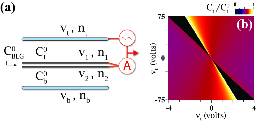
As we discuss in detail below, the layer population asymmetry, Eq.(2), manifests itself in capacitance measurements. This is illustrated in Fig.1(b), in which top-gate capacitance found using a self-consistent model (see Sec.IV) is plotted as a function of gate voltages and . The enhancement in capacitance associated with the band edge is stronger when the divergent vHs-bearing layer is facing the gate used to measure capacitance (top layer for and bottom layer for in Fig. 1 a). We refer to this behavior as ‘near-layer capacitance enhancement’ (NLCE). This NLCE effect is seen in the capacitance map shown in Fig.1(b): the dark region, corresponds to the insulating state realized when the chemical potential is positioned inside field-induced gap, is bordered on one side by a bright fringe corresponding to the NLCE. The markedly different contrast between the van Hove singularity- associated features positioned on either side of the dark region, is associated with the density piling up on the near layer rather than the far one.
This behavior explains the asymmetry observed in top-gate capacitance measurements [Young2010, ], in which a feature identified with the vHs was observed only for electrons (holes) when the high (low) energy layer was nearest the gate from which capacitance was measured. In contrast, no such asymmetry is expected for the capacitance measured using ‘penetration field’ geometryHenriksen2010 , because the penetration field capacitance is more symmetric than the one-sided (top or bottom) gate capacitance. Indeed, no NLCE-type asymmetry was observed in the measurements reported in Ref.[Henriksen2010, ]. As we shall see, the gate capacitance and the penetration field capacitance measure fundamentally different characteristics of the system. Simultaneous measurements of gate and penetration field capacitances can thus provide detailed and direct information on layer polarization of the bilayer.
The NLCE effect is sensitive to the form of the vHs, which depends on the specifics of the dispersion relation. The simplest model for BLG, which we focus on below, is that of quartic dispersion, described by the Hamiltonian (1). A more detailed analysis McCann2006prl ; McCann2006prb ; Castro2007 , based on the four band model, leads to a ‘Mexican hat’ structure in band dispersion near points and . However, the Mexican hat dispersion and the quartic dispersion both lead to an inverse square-root vHs at the band edge, resulting in essentially identical NLCE effects.
In this paper we develop theory of the NLCE effect. In section III we calculate, using a two band model of BLG, layer-indexed densities of states, , where refer to the two layers. In section IV we develop a many-body approach that describes interactions of particles in BLG with other particles and also with gate potentials. Using a self-consistent Hartree-type approximation, we derive expressions for several quantities of interest relevant to capacitance measurements in terms of the matrix elements . We find that different experimental observables exhibit very different behavior. In particular, the gate capacitance exhibits strong particle-hole asymmetry and the NLCE effect (see Fig.1), while the penetration-field capacitance is nearly particle-hole symmetric. In section V, we consider the effect of disorder, and show that the asymmetry persists for relatively high disorder concentrations corresponding to the experimental regime. Finally, we conclude with a discussion of the usefulness of different capacitance measurements in bilayer graphene for probing the layer-pseudospin texture of possible broken symmetry phases.
III The van Hove singularities and compressibility in clean BLG
The main features of the compressibility of BLG in an external field can be understood in terms of the many-body Hamiltonian
| (3) |
where is the single-particle Hamiltonian (1) and summation over four flavors accounts for the spin and valley (, ) degrees of freedom. The interaction is written in terms of density harmonics on the layers, (),
| (4) |
with and the intralayer and interlayer Coulomb interaction,
| (5) |
where is the interlayer spacing in BLG.
We analyze quantum corrections to the capacitance of gated BLG described by the Hamiltonian (3) using a Hartree-type approximation. This is done in two steps. We first find the compressibility matrix of non-interacting fermions, formally setting in Eq.(3). In doing this, the BLG potentials and are treated as external parameters. Next, in Sec.IV, we restore the interaction , adding to it the interaction between all charges, including those on the gates. We relate potentials to charges on the gates and the graphene bilayer self-consistently, and use these relations to evaluate capacitance as a function of external gate voltages.
The Hartree-type analysis presented in this paper does not account for correlation effects; however, estimates of the correlation energy and the analysis of compressibility of BLG presented in Ref.[Nandkishore2010, ] indicate that the corresponding correction to capacitance is small, except at very low values of disorder and temperature, where the BLG system develops an instability towards a correlated state.
In recent experiments Henriksen2010 ; Young2010 electronic states with different doping relative to the neutrality point are probed by varying the potentials and through their response to the potentials and applied to external gates. Metallic and insulating conductance regimes occur when the Fermi level lies inside or outside the gate-induced gap Oostinga2008 ; Zou2010 ; Taychatanapat2010 . The insulating regime was observed to accompany a drop in compressibility.
It is convenient to introduce layer-symmetrized potentials . Within the two band model (1), the gap size is and the position of the gap center relative to the Fermi level is ; the metallic and insulating regimes in a clean bilayer are then described by and , respectively. In experiments Henriksen2010 ; Young2010 capacitance was measured with the graphene bilayer grounded. This situation can be described by a Fermi level pinned to zero energy, .
Particle densities on the two layers can be expressed as sums over all occupied states,
| (6) |
where . In what follows, we focus on the case of zero temperature, . Using the eigenstates of the Hamiltonian (1) and defining layer-symmetrized densities , we find
| (7) | |||
| (8) |
where is an ultraviolet cutoff of order the bandwidth. Here accounts for the four-fold spin/valley degeneracy, and can be written as , where is the Bohr’s radius of BLG. The two cases in Eqs.(7),(8), metallic and insulating, correspond to the regimes and .
Using these expressions we can compute the entries of the compressibility matrix . The expressions have different form for and for :
| (9) | |||
| (10) | |||
| (11) |
where we defined
| (12) |
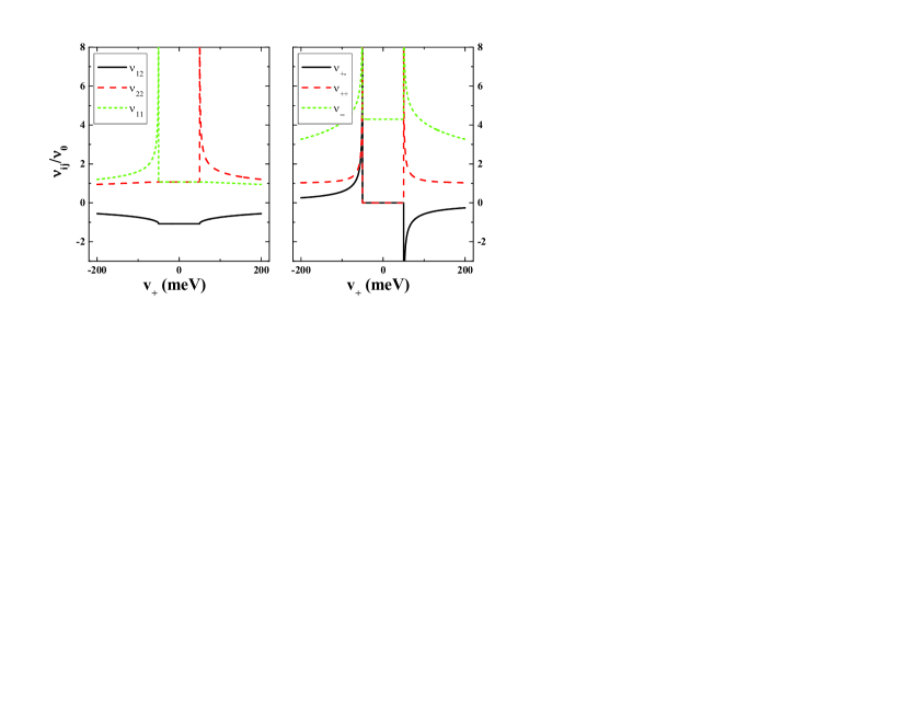
with . Expressions (9)-(11) are plotted in the left panel of Fig. 2. Note that the compressibility matrix is symmetric, .
Different elements of matrix have different physical meanings. The diagonal element is the total charge compressibility. The diagonal element is layer polarizability. The off-diagonal elements describe the charge-flavor response. The latter quantities are particularly useful, as they measure the layer distribution of incremental additions of charge, giving information about the layer polarization of the ground state: the quantities and are zero for an unpolarized bilayer, but nonzero in the presence of a charge imbalance.
Rewriting Eqs.(7),(8) in terms of variables characterizing individual layers, , , we obtain
| (13) | |||
| (14) | |||
| (15) |
Expressions (13)-(15) are invariant under simultaneous exchange and gap inversion, .
Both of the diagonal compressibility matrix elements ( and ) exhibit an inverse square root divergence at the charge gap edge, where the density of single particle states has a van Hove singularity. The two diagonal compressibilities behave asymmetrically, diverging on opposite sides of the gap: diverges at , while diverges at . In contrast, the off-diagonal compressibilities () remain finite on either side of the charge gap and are symmetric (see Fig. 2, left panel). Inside the charge gap, , the diagonal and off-diagonal compressibilities are constant:
| (16) |
exhibiting no divergence at the gap edge.
IV Self-consistent capacitance calculation
We shall focus on the geometry pictured in Fig.1a, which describes a dual-gated graphene device of the type studied in Refs.[Young2010, ] and [Henriksen2010, ]. The experimental system consists of a bilayer graphene sheet placed between two gates, characterized by potentials and , charge densities and , and geometric capacitances to the bilayer and . The bilayer is described by the potentials and and charge densities and induced by the external gates on the individual layers. Electrostatic energy of the bilayer itself is taken into account by including an interlayer capacitance , which can be estimated from the “geometric” value obtained for a parallel plate capacitor, , with . This electrostatic model amounts to the approximation that the charge density on the bilayer is of the for m . While corrections are expected due to the finite extent of the wavefunctions, these corrections amount, for the most part, to a renormalization of , upon which our results do not sensitively depend.
The quantities of interest obey the general electrostatic charge field relations
| (17) | |||
| (18) | |||
| (19) | |||
| (20) |
To complete the system of equations for charge densities and potentials, a set of constitutive relations for BLG must be used. These relations, which are of general form , , will be calculated in subsequent sections.
Capacitance measurements are done in the finite frequency regime, by applying a small AC bias (on top of the DC bias used to control density and interlayer imbalance) to one terminal of the device and then recording the resulting change in charge density on a second terminal. Choice of terminals distinguishes top (back) gate capacitance, , from penetration field capacitance, ,
| (21) |
After eliminating and from Eqs. (17)-(20) by expressing them in terms of other variables, , , the remaining two equations are linearized with the help of the matrix of inter- and intralayer compressibilities
| (22) |
This yields
| (23) |
where is a matrix of geometric capacitances,
| (24) |
These expressions account for both the geometric and ‘intrinsic’ capacitance of BLG.
Solving for , , we find the charges induced on each layer by the gate potentials:
| (29) |
Here the first term describes the geometric capacitance, which would be the only contribution if the electronic system in BLG was infinitely compressible, . The term proportional to describes the quantum capacitance contribution. Combining equation (29) with the relations for and , all three capacitance observables can be calculated:
| (30) | ||||
| (31) | ||||
| (32) |
These quantities implicitly depend on the gate potentials through the compressibility matrix .
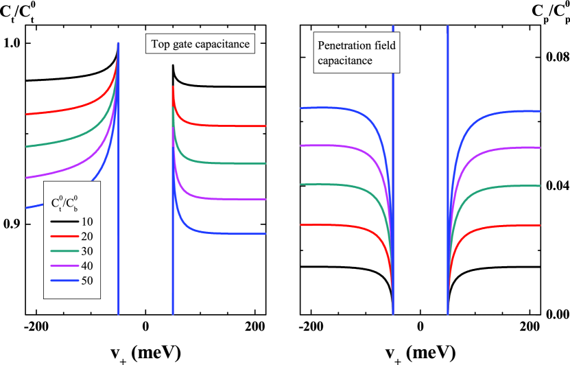
Notably, different capacitance observables depend on different combinations of the compressibility matrix elements, and obey different symmetries. The penetration field capacitance is dominated by the off diagonal component of the (necessarily symmetric) compressibility matrix. As a result, for a symmetric device () it is invariant under interchanging layers 1 and 2 and therefore does not exhibit the NLCE effect. In contrast, the expressions for and are not invariant. In particular, the last term in the expression for , proportional to , changes to upon layer permutation. As shown in the previous section, in the presence of a layer imbalance these two quantities are not the same, leading to the observed NLCE observed in Ref.Young2010, .
In a device in which all capacitances can be measured, combinations of the measured quantities can be combined to probe the charge-flavor response. For the simplest case of a symmetric gate configuration (),
| (33) |
Because this quantity is proportional to , it can be used to probe both gate-induced and spontaneous layer polarization, allowing direct experimental measurement—somewhat analogous to Knight Shift measurements for spin—of the ground state layer polarization.
V The effect of disorder
In the devices used for capacitance measurements in Refs.[Young2010, ],[Henriksen2010, ], graphene flakes were supported by a silica substrate. The carrier mobility in such devices was of order 1,000 cm2/V sec. For such low-mobility devices, taking into account the effect of disorder is crucial for developing a sensible model of the experimental data. Full quantitative description of experiments requires including realistic disorder, which is likely long range Nilsson2007 ; Nilsson2008 ; Abergel2011 , along with the effects of electronic correlations Borghi2010 which can give quantitative corrections to the electronic compressibility. However, the the key features of the data are captured by a simpler short range disorder model Mkhitaryan2008 , which involves delta-function impurities localized on carbon sites:
| (34) |
with potential taking values on the carbon sites occupied by impurities, and zero elsewhere. The impurities are assumed to be distributed randomly with concentration .
The problem (34) can be analyzed using a self-consistent T-matrix approximation (SCTA). The SCTA approach provides a somewhat more general approach than the self-consistent Born approximation, and is reduced to the latter for weak disorder.
We evaluate the DOS and the total energy by employing disorder-averaged Greens functions expressed through the layer-indexed disorder-averaged self-energies
| (35) |
where tp is the kinetic energy operator McCann2006prl ; McCann2006prb ; Castro2007 , . An infinitesimal imaginary part should be added to to obtain the retarded and advanced Greens functions.
The self-energy is approximated by the average values of the -matrix, evaluated separately for the sites on layers and ,
| (36) |
Here is the adatom density with the density of type sites. The quantities , written as a matrix, are given by
| (37) |
where . For realistic values of and the integral of the Greens function over the Brillouin zone is dominated by the regions near and ; approximating , we obtain
| (38) |
This expression is valid for small compared to the bandwidth. Combining this result with Eq.(36), we obtain two coupled equations for , :
| (39) |
where we defined and . Solving these equations for , as a function of , we find the Greens function (35) and use it to calculate the density of states,
| (40) |
where the integral is identical to the one in Eq.(38). A factor of two was inserted after integration to account for spin degeneracy.
The density of states is expressed through the quantity . Taking the ratio of the self-consistent equations for and , Eq.(39), we obtain a single equation for the quantity . Focusing on the case of weak disorder potential and expanding in , we arrive at
| (41) |
where the terms linear in have been incorporated in the quantities . Once is found from Eq.(41), it can be plugged into Eq.(40) to obtain partial densities of states on each of the layers (see Fig.3),
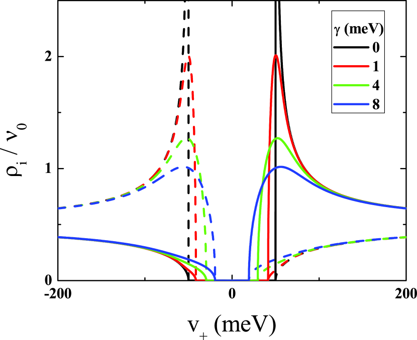
| (42) |
In the absence of disorder, , we have , which gives van Hove singularities of an inverse square root form at the band edges as found in section I. In the presence of disorder, these singularities are washed out to varying degrees. As shown in Fig.4, this washing out proceeds by both reducing the height of the vHs peak and closing the gap. Crucially, the ‘off’-layer density of states at the energy of the ‘on’ layer vHs peak increases with disorder. This has the effect of increasing the screening effect of the ‘off’ layer when it lies closer to the gate used to measure capacitance, enhancing the NLCE effect for disordered samples.
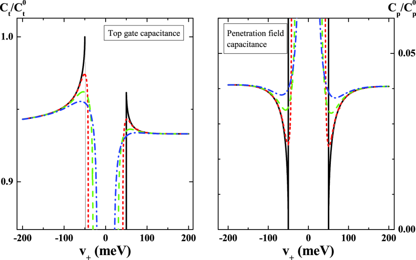
To calculate experimental capacitances, Eqs. (31)-(32), the partial densities of states are integrated numerically with respect to energy and then redifferentiated with respect to the appropriate energy variable, or . In Figure 5, the results for both top gate and penetration field capacitance for a device with electrostatic parameters resembling those in Ref.Young2010, are plotted. The asymmetry of top gate capacitance survives disorder averaging, and indeed is enhanced. For intermediate values of disorder, electrons and holes display qualitatively different behavior: the non-monotonic vHs feature survives for holes but is completely obliterated for electrons, as observed in Ref.Young2010, .
VI Conclusions
As we argue above, electrostatic capacitance measurements offer a unique which-layer probe for BLG. The sensitivity to the interlayer imbalance arises despite the fact that the layers are not contacted separately: the relative proximity of the layers to the top- and bottom- gates, combined with the interlayer screening, allows capacitance measurements to access layer specific quantities. Gate capacitance measurements preferentially probe the nearer layer, leading to the NLCE effect as the near layer screens the far layer. Consequently, in the presence of a layer imbalance, top- and bottom- gate capacitance measurements will be different. This difference is the signature of layer polarization, allowing its unambiguous experimental determination.
Our analysis provides an explanation of recent top gate capacitance experiments on dual gate bilayer graphene structures Henriksen2010 ; Young2010 . Since the degeneracy of the band crossing in the BLG spectrum at the and points is linked to inversion symmetry, the gate-induced density imbalance and the opening of a band gap go hand in hand McCann2006prl ; McCann2006prb ; Castro2007 . As we have shown, this imbalance can be probed directly through NLCE measurements; to our knowledge, the NLCE-type asymmetry observed in Ref.Young2010, is the first direct experimental evidence of layer imbalance in BLG.
The possibility of probing layer polarization directly through capacitance measurements has implications beyond the study of gate-induced gap opening. Recently, experimental sample quality has improved to the point of allowing the observation of a multitude of novel features likely associated with electronic correlations Feldman2009 ; Zhao2010 ; Dean2010 ; Martin2010 ; Weitz2010 . A large number of possible broken symmetry states, arising in the presence and in the absence of magnetic field, have been explored in the theoretical literature Barlas2008 ; Vafek2009 ; Min2008prb2 ; Nandkishore2009 ; Lemonik2010 ; Jung2010 ; Zhang2010 ; Cote2010 ; Nandkishore2010 , including several mutually exclusive scenarios for the ordering at low densities and small electric and magnetic fields. The main open questions pertaining to these states have to do with identifying broken symmetries and determining the exact structure of the order parameter and excitations. Future NLCE measurements, by offering a direct method for determination of the layer polarization, will help to narrow down the possibilities for these new states.
Acknowledgements.
We thank P. Kim and R. Nandkishore for useful discussions. This work was supported by Office of Naval Research Grant No. N00014-09-1-0724 and the Department of Energy under DOE (DE-FG02-05ER46215).References
- (1) S. Luryi, Applied Physics Letters 52, 501 (1988).
- (2) M. S. Bello, E. I. Levin, B. I. Shklovskii, and A. L. Efros, Sov. Phys JETP 53, 822 (1981).
- (3) J. P. Eisenstein, L. N. Pfeiffer, and K. W. West, Phys. Rev. Lett. 68, 674 (1992).
- (4) J. P. Eisenstein, L. N. Pfeiffer, and K. W. West, Phys. Rev. B 50, 1760 (1994).
- (5) S. Ilani, L. A. K. Donev, M. Kindermann, and P. L. McEuen, Nature Physics 2, 687 (2006).
- (6) S. C. Dultz and H. W. Jiang, Phys. Rev. Lett. 84, 4689 (2000).
- (7) S. Ilani, A. Yacoby, D. Mahalu, and H. Shtrikman, Science 292, 1354 (2001).
- (8) B. Skinner and B. I. Shklovskii, Phys. Rev. B 82, 155111 (2010).
- (9) L. Li et al., Science 332, 825 (2011).
- (10) L. A. Ponomarenko et al., Phys. Rev. Lett. 105, 136801 (2010).
- (11) E. A. Henriksen and J. P. Eisenstein, Phys. Rev. B 82, 041412 (2010).
- (12) A. F. Young et al., arxiv:1004.5556 (2010).
- (13) J. Xia, F. Chen, J. Li, and N. Tao, Nature Nanotechnology 4, 505 (2009).
- (14) J. Martin et al., Nature Physics 4, 144 (2008).
- (15) J. Martin et al., Nature Physics 5, 669 (2009).
- (16) D. S. L. Abergel, P. Pietiläinen, and T. Chakraborty, Phys. Rev. B 80, 081408 (2009).
- (17) Y. Barlas, R. Côté, K. Nomura, and A. H. MacDonald, Phys. Rev. Lett. 101, 097601 (2008).
- (18) O. Vafek and K. Yang, Phys. Rev. B 81,, 041401(2010) (2009).
- (19) H. Min, G. Borghi, M. Polini, and A. H. MacDonald, Phys. Rev. B 77, 041407 (2008).
- (20) R. Nandkishore and L. Levitov, Phys. Rev. Lett. 104, 156803 (2010).
- (21) Y. Lemonik, I. Aleiner, C. Toke, and V. Fal’ko, Arxiv:1006:1399 (2010).
- (22) J. Jung, F. Zhang, and A. H. MacDonald, arxiv:1010.1819.
- (23) F. Zhang, H. Min, M. Polini, and A. H. MacDonald, Phys. Rev. B 81, 041402 (2010).
- (24) R. Cote et al., arXiv:1010.0364.
- (25) R. Nandkishore and L. Levitov, arXiv:1002.1966 (2010).
- (26) J. Martin et al., Phys. Rev. Lett. 105, 256806 (2010).
- (27) E. McCann and V. I. Fal’ko, Phys. Rev. Lett. 96, 086805 (2006).
- (28) E. McCann, Phys. Rev. B 74,, 161403 (2006).
- (29) E. V. Castro et al., Phys. Rev. Lett. 99, 216802 (2007).
- (30) J. B. Oostinga et al., Nature Materials 7, 151 (2008).
- (31) K. Zou and J. Zhu, Phys. Rev. B 82, 081407 (2010).
- (32) T. Taychatanapat and P. Jarillo-Herrero, Phys. Rev. Lett. 105, 166601 (2010).
- (33) J. Nilsson and A. H. Castro Neto, Phys. Rev. Lett. 98, 126801 (2007).
- (34) J. Nilsson, A. H. Castro Neto, F. Guinea, and N. M. R. Peres, Phys. Rev. B 78, 045405 (2008).
- (35) D. S. L. Abergel, E. H. Hwang, and S. Das Sarma, Phys. Rev. B 83, 085429 (2011).
- (36) G. Borghi, M. Polini, R. Asgari, and A. H. MacDonald, Phys. Rev. B 82, 155403 (2010).
- (37) V. V. Mkhitaryan and M. E. Raikh, Phys. Rev. B 78, 195409 (2008).
- (38) B. E. Feldman, J. Martin, and A. Yacoby, Nature Physics 5, 889 (2009).
- (39) Y. Zhao, P. Cadden-Zimansky, Z. Jiang, and P. Kim, Phys. Rev. Lett. 104, 066801 (2010).
- (40) C. R. Dean et al., Nature Nanotechnology 5, 722 (2010).
- (41) R. T. Weitz et al., Science 330, 812 (2010).