Disorder-induced temperature-dependent transport in graphene: Puddles, impurities, activation, and diffusion
Abstract
We theoretically study the transport properties of both monolayer and bilayer graphene in the presence of electron-hole puddles induced by charged impurities which are invariably present in the graphene environment. We calculate the graphene conductivity by taking into account the non-mean-field two-component nature of transport in the highly inhomogeneous density and potential landscape, where activated transport across the potential fluctuations in the puddle regimes coexists with regular metallic diffusive transport. The existence of puddles allows the local activation at low carrier densities, giving rise to an insulating temperature dependence in the conductivity of both monolayer and bilayer graphene systems. We also critically study the qualitative similarity and the quantitative difference between monolayer and bilayer graphene transport in the presence of puddles. Our theoretical calculation explains the non-monotonic feature of the temperature dependent transport, which is experimentally generically observed in low mobility graphene samples. We establish the 2-component nature (i.e., both activated and diffusive) of graphene transport arising from the existence of potential fluctuation induced inhomogeneous density puddles. The temperature dependence of the graphene conductivity arises from many competing mechanisms, even without considering any phonon effects, such as thermal excitation of carriers from the valence band to the conduction band, temperature dependent screening, thermal activation across the potential fluctuations associated with the electron-hole puddles induced by the random charged impurities in the environment, leading to very complex temperature dependence which depends both on the carrier density and the temperature range of interest.
pacs:
72.80.Vp, 72.10.-d, 73.22.Pr, 81.05.ueI Introduction
Graphene, as a novel gapless two dimensional (2D) chiral electron-hole system, has attracted great interest in recent years, both experimentally and theoreticallyDas Sarma et al. (2011); Castro et al. (2007). Its transport properties have been at the center of key fundamental and technological efforts with vast potential for applications in future nanotechnologyLee et al. (2010). For monolayer graphene (MLG), the fundamental interest arises from its unique linear chiral Dirac carrier dispersion with a zero energy gap between conduction and valence bandNovoselov et al. (2005). The bilayer graphene (BLG) is also intriguing as its physical properties lie between MLG and 2D semiconductor-based electron gas (2DEG) systems which are gapped and non-chiral with a quadratic band dispersion. Much of the early work on graphene transport focused on the density-dependent (i.e., gate voltage tuned)Das Sarma et al. (2011); Novoselov et al. (2005); Tan et al. (2007a); Chen et al. (2008a); Hong et al. (2009); Chen et al. (2009) and temperature-dependent Das Sarma et al. (2011); Tan et al. (2007b); Chen et al. (2008b); Hwang and Das Sarma (2009); Lv and Wan (2010) conductivity in homogeneous MLG and BLG systems. The basic graphene transport properties, particularly at high densities far from the charge neutral Dirac point, are now reasonably well-understoodDas Sarma et al. (2011).
However, unintended charged impurities, which are invariably present in the graphene environment, (e.g., the substrate-graphene interface), lead to the formation of inhomogeneous electron-hole puddles in the system Hwang et al. (2007); Rossi et al. (2009), which have been confirmed by experimentsMartin et al. (2008); Zhang et al. (2011) using the techniques of scanning potential and tunneling microscopies. Although MLG samples show a metallic behavior at high densities a weak “insulating” temperature-dependent conductivity has been measured at low carrier density and at the charge neutrality point (CNP) Tan et al. (2007b). (We define insulating/metallic temperature dependence of conductivity as being positive/negative at fixed gate voltage.) In addition, a recent experimentHeo et al. (2011) on low mobility MLG grown by chemical vapor deposition (CVD) shows a strong “insulating” behavior at low temperatures and a metallic feature at high temperatures manifesting a non-monotonic temperature dependence in the measured electrical conductivity. In BLG samples Zhu et al. (2009); Feldman et al. (2009); Zou and Zhu (2010); Nam et al. (2010) the strong insulating behavior in the temperature dependent conductivity has been observed not only near CNP but also at carrier densities as high as cm-2 or higher. To be more specific, in Ref. [Zhu et al., 2009], in BLG increases by as temperature increases from K for carrier density in the range cm-2. To understand this anomalous temperature dependence in , both MLG and BLG, it is essential to know the role of disorder in graphene transport. We note that phonon scattering (Ref. [Hwang and Das Sarma, 2008a; Min et al., 2011]), although being weak in graphene, always contributes an increasing resistivity with increasing temperature and thus always leads to metallic behavior, and thus cannot be the mechanism for the intriguing insulating temperature dependence often observed in graphene transport at lower carrier densities – in fact, at very high temperatures ( K) graphene should always manifest metallic temperature dependence in its conductivity due to phonon scattering effects which we would ignore in the current work. Our goal here is to theoretically study in a comprehensive manner the temperature dependence of graphene transport properties arising entirely from the disorder effects.
The experimentally measured anomalous temperature dependent conductivity of BLG has been theoretically investigated by applying the analytic statistical theory to the inhomogeneous potential fluctuation and it is found that the anomalous BLG is likely to be caused by the electron-hole puddles induced by randomly distributed disorder in the graphene environment Hwang and Das Sarma (2010). In this paper, we extend this work and apply the same analytic statistical theory to MLG systems and explain the intriguing coexistence of both metallic and insulating features of MLG . In the presence of large fluctuating potentials associated with microscopic configurations of Coulomb disorder in the system, the local Fermi level, , would necessarily have large spatial fluctuations. We carry out an analytical theory implementing this physical idea by assuming that the value of the potential at any given point follows a Gaussian distribution, parametrized by (the root-mean-square fluctuations or the standard deviation in about the average potential). This distribution can then be used to average the local density of states to obtain effective carrier densities, which can then be used to compute the physical quantities of interestAbergel et al. (2011). The observed anomalous temperature dependent is then understood as the competition between the thermal activation of carrier density and temperature-dependent screening effects. Our theory explains the suppression of the insulating behavior in higher mobility samples with lower disorder, which is consistent with experimental observations. We also provide the similarity and the quantitative difference between monolayer and bilayer graphene transport in the presence of puddles.
The motivation of our theory comes from the observation that the electron-hole puddles, which dominate the low-density graphene landscape, allow for a 2-component semiclassical transport behavior, where the usual metallic diffusive carrier transport is accompanied by transport by activated carriers which have been locally thermally excited above the potential fluctuations imposed by the static disorder. This naturally allows for both insulating and metallic transport behavior occurring preferentially respectively at lower and higher carrier densities since the puddles disappear with increasing carrier density due to screening. At zero temperature (where no activation is allowed) or at very high carrier density (where puddles are suppressed), only diffusive transport is possible. But at any finite temperatures and at not too high densities, there would always be a 2-component transport with both activated and diffusive carriers contributing to conductivity. Our theory develops this idea into a concrete description. We emphasize that our theory explicitly takes into account the inhomogeneous nature of the graphene landscape and is non-mean-field as a matter of principle.
This paper is organized as follows. In Sec. II, we introduce the analytical statistical theory to describe random electronic potential fluctuations created by charged impurities in the environment. We also calculate the modified density of states and the corresponding temperature-dependent effective carrier density in monolayer graphene. Then, in Sec. III, we describe the calculations and the main features of the temperature-dependent conductivity of MLG in the presence of density inhomogeneity. In Sec. IV and V, we elaborate and extend our earlier results for the interplay between density inhomogeneity and temperature in bilayer graphene (BLG) transport. We further discuss the connection of our theory to earlier theories in Sec. VI. We discuss the similarities and quantitative differences among the effects of inhomogeneity (i.e., the puddles) on MLG and BLG transport and summarize our results in Sec. VII. In Appendix A, we discuss a microscopic theory to calculate the effects of potential fluctuation on graphene systems, providing a self-consistent formulation of graphene density of states in the presence of random charged impurities near graphene/substrate interface, showing in the process that this microscopically calculated density of states agrees well with the model density of states obtained from the Gaussian fluctuations.
II Temperature dependent carrier density for inhomogeneous MLG
It is well known that MLG breaks up into an inhomogeneous landscape of electron-hole puddles, especially around the charge neutral point (CNP) Martin et al. (2008); Rossi and Das Sarma (2008); Zhang et al. (2011). Below we derive an analytic statistical theory taking account of the effects of inhomogeneous density in monolayer graphene (MLG) to explain the nonmonotonic temperature dependent transport observed in MLG Tan et al. (2007b); Heo et al. (2011). We start by assuming that charged impurities, located in the substrate or near the graphene, create a local electrostatic potential, which fluctuates randomly about its average value across the surface of the graphene sheet. The potential fluctuations themselves are assumed to be described by a statistical distribution function where is the fluctuating potential energy at the point in the 2D MLG plane. We approximate the probability of finding the local electronic potential energy within a range about to be a Gaussian form, i.e.,
| (1) |
where is the standard deviation (or equivalently, the strength of the potential fluctuation), which is used as an adjustable parameter to tune the tail-widthArnold (1974). In the Appendix, we provide a microscopic approach to self-consistently solve the strength of potential fluctuations in the presence of charged impurities. Due to the electron-hole symmetry in the problem, we only provide the formalism and equations for electron like carriers and the hole part can be obtained simply by changing to .
The potential fluctuations given by Eq. (1) affect the overall electronic density of states (DOS) in MLG. In our model we do not assume that the size of the puddles to be identical, but we take the puddle sizes to be completely random controlled by the distribution function given in Eq. 1. We emphasize that our assumption of a Gaussian distribution for the potential fluctuations, equivalently implying a Gaussian distribution for the density fluctuations associated with the puddles, is known to be an excellent quantitative approximation to the actual numerically calculated puddle structures in grapheneDas Sarma et al. (2011); Rossi and Das Sarma (2008). The characteristics of the puddles are determined by both the sign and the magnitude of , i.e., a negative (positive) indicates an electron (hole) region. A different approach utilizing equal size puddles with a certain potential has been used to calculate transport coefficients using a numerical transfer matrix technique San-Jose et al. (2007). Then in the presence of electron-hole puddles the density of states is increased by the allowed electron region fraction and given by Zallen and Scher (1971); Eggarter and Cohen (1970); Arnold (1974)
| (4) |
where erfc is the complementary error function,
| (5) |
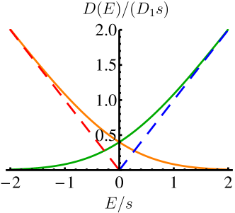
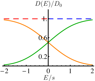
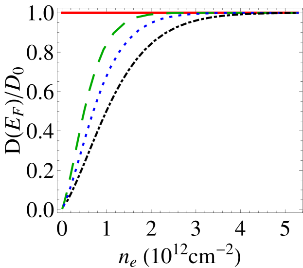
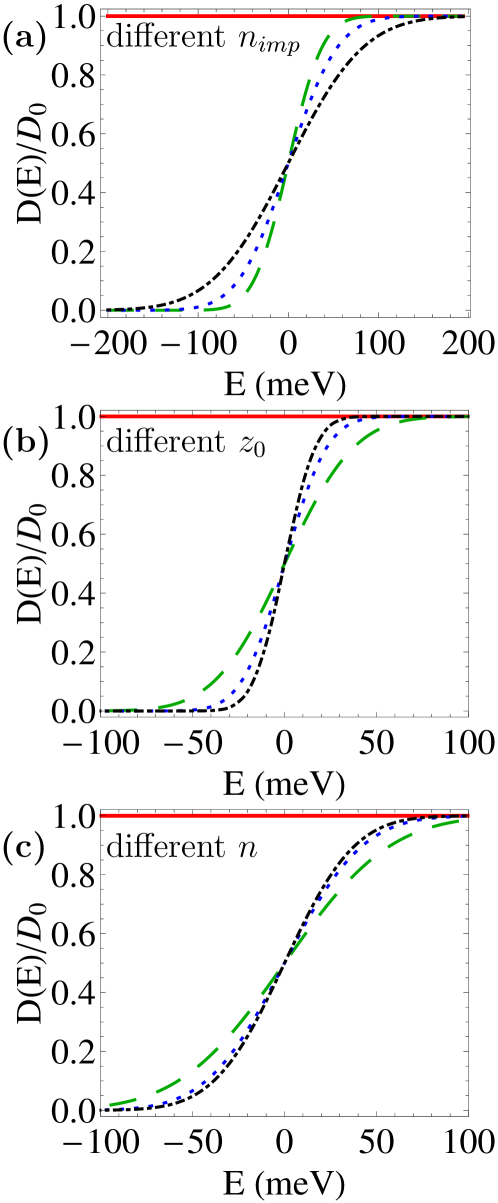
and , where is the graphene Fermi velocity, and are the spin and valley degeneracies, respectively. We have cm-2/meV2 with the Fermi velocity m/s. Note that the tail of the DOS is determined by the potential fluctuation strength . For the case , the system becomes homogeneous and . In this case there is no carrier density at Dirac point () at zero temperature. It is apparent that in the presence of potential fluctuations, the starts at finite value at and approaches in high energy limit. For high-energy limit, the carrier is essentially free since nearly every point of the system is accessible. In Fig. 1, we show the normalized density of states as a function of energy for both electrons and holes in MLG. We mention that the self-consistent microscopic theory gives the same structure for the density of states of graphene systems (see Appendix A).
Since monolayer graphene is a semi-metal or zero-gap semiconductor, the electron density at finite temperatures increases due to the direct thermal excitation from valence band to conduction band, which is one of the important sources of temperature dependent transport at low carrier densities. Therefore, we first consider the temperature dependence of thermally excited electron density. The total electron density is given by
| (6) |
where and is the chemical potential. At , becomes the Fermi energy .
II.1 of MLG at CNP ()
When the Fermi energy is zero (or at CNP) all electrons are located in the band tail at and the electron and hole densities in the band tail are given by
| (7) |
Note that the electron (or hole) density in the band tails increases quadratically with the standard deviation . At finite temperatures the behavior of at CNP becomes
| (8) |
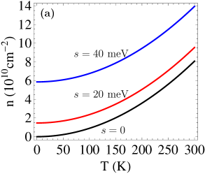
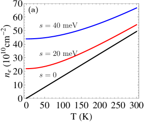
The leading order temperature dependence in is quadratic. For homogeneous MLG () with the linear-in-energy behavior of the DOS, the electron density is given by . In particular, in the ballistic regime the number of propagating channels increases due to the thermal smearing of the Fermi surface, which leads to the observation of an insulating behavior in at CNP for high mobility suspended graphene samplesDu et al. (2008); Bolotin et al. (2008); Müller et al. (2009). The presence of the band tail does not change the quadratic temperature dependence in the thermal excitation when the system is at the charge neutral point (). But the inhomogeneous MLG has electrons in the band tails. In Fig. 2(a) we show the temperature dependent electron density at CNP for different values of standard deviation .
II.2 of MLG at finite doping ()
In the case of finite doping (or gate voltage), i.e., , the electron density of the homogeneous MLG (i.e., ) is given by
| (11) |
where , and is the chemical potential of homogeneous MLG and is determined by the conservation of the total electron density. Then the chemical potential is given by the following relation, . Using the asymptotic forms Hwang and Das Sarma (2009) of the function for and , i.e.,
| (12) |
we have the asymptotic formula for the chemical potential in both low- and high-temperature limits for homogeneous MLG
| (13) |
Then the corresponding asymptotic formula of the electron density (Eq. 11) are given by
| (14) |
Since the direct thermal excitation is suppressed due to the finite Fermi energy, the excited electron density at low temperatures () increases quartically rather than quadratically. But at high temperatures (), the total electron density becomes a quadratic function of temperature as shown for an undoped MLG.
Next, we derive the temperature dependence of thermally excited electron density in the presence of electron-hole puddles () at finite doping (). At zero temperature the electron density for the inhomogeneous MLG can be written as:
| (18) |
where . The presence of electron-hole puddles does not induce any additional charge in the MLG system and the net carrier density should be conserved. Then, the finite temperature chemical potential changes as a function of both temperature and the strength of potential fluctuation , and it should satisfy the following relation:
| (19) |
where is the electronic density of states given by Eq. 4 and is the density of states for holes. The asymptotic analytical formula of the chemical potential for inhomogeneous MLG is obtained as:
| (20) |
where functions and are given as follows:
| (21) |
where and is the error function.
Combining Eqs. 4, 6 and 20, we obtain the asymptotic analytical formula of the electron density for inhomogeneous MLG at low- and high-temperature limits as:
| (25) |
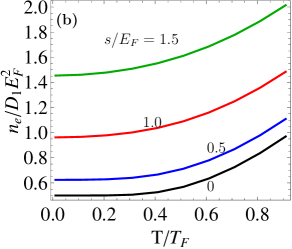
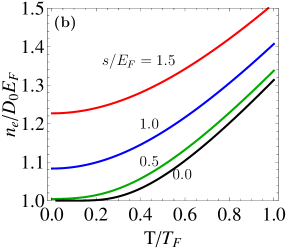
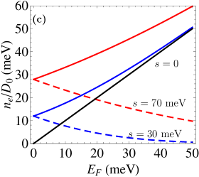
In the low temperature limit (), the leading order term for the electron density has the same quadratic behavior as in undoped homogeneous MLG (), but the coefficient is strongly suppressed by fluctuation for the case of , i.e., the high carrier density sample. While in the case of , i.e., the low carrier density sample, the existence of electron-hole puddles gives rise to a notable quadratic behavior for electron density [see Fig. 2(b)].
III Conductivity of inhomogeneous MLG
In this section, we calculate the finite temperature conductivity for inhomogeneous MLG with the temperature-dependent effective carrier density derived above. The existence of electron-hole puddles allows that the current flows through “percolation channels” and the transport properties of the inhomogeneous MLG system can be derived using the self-consistent effective medium theory of conductance in composite mixturesKirkpatrick (1973), where the number of electrons per puddle is not an important issue for our theory. The percolation assumption is valid as long as the potential fluctuation is larger than the thermal energy of the carriers. Otherwise transport due to disorder scattering dominates. We emphasize that in our formalism the crossover from the percolation transport to ordinary scattering-dominated diffusive transport is guaranteed as the temperature is increased since we are explicitly taking into account both diffusive transport of free carriers and activated transport of the classically-localized carriers in our theory. The only effects we neglect are quantum tunneling through the potential barriers and quantum interference since ours is a semiclassical theory. We also do not consider Klein tunneling explicitly in this paper because the Klein tunneling occurs at zero temperature for normal incident carriers at the electron-hole puddle boundary. We also apply the Boltzmann transport theory, where we include the scattering mechanism with screened Coulomb impurities and short-range disorderHwang and Das Sarma (2009). Note that the application of Boltzmann transport theory is justifiable because the quantum interference effects are not experimentally observed in the temperature regime of interest to us in this work. It is conceivable that quantum interference and localization play some roles in graphene transport at very low temperatures, which is beyond the scope of this paper. We also neglect all phonon effects in this work since electron-phonon coupling is weak in graphene. Phonon effects are relevant at high temperatures ( K) and have been considered in the literatureHwang and Das Sarma (2008a); Min et al. (2011).
At CNP () electrons and holes are equally occupied. As the Fermi energy increases, more electrons occupy increasingly larger proportion of space. As the Fermi energy increases to , nearly all space is populated by the electrons [see Fig. 2(c)] and the conductivity of the system approaches the characteristic of the homogeneous material. Thus, there is a possible coexistence of metallic and thermally-activated transport in the presence of electron-hole puddles. When electron puddles occupy more space than hole puddles, most electrons follow the continuous metallic paths extended throughout the system, but it is possible at finite temperatures that the thermally activated transport of electrons persists above the hole puddles. On the other hand, holes in hole puddles propagate freely, but when they meet electron puddles, activated holes conduct over the electron puddles. Carrier transport in each puddle is characterized by propagation of weak scattering transport theoryKirkpatrick (1973). The activated carrier transport of prohibited regions, where the local potential energy is less (greater) than Fermi energy for electrons (holes), is proportional to the Fermi factor. If and are the average conductivity of electron and hole puddles, respectively, then the activated conductivities are given by
| (26a) | |||||
| (26b) | |||||
where the density and temperature dependent average conductivities ( and ) are given within the Boltzmann transport theory Das Sarma et al. (2011) by and , where and are average electron and hole densities, respectively, and is the average transport relaxation time which includes the thermal smearing effects and depends explicitly on the scattering mechanism Das Sarma et al. (2011) and it is given by,
| (27) |
where and are, respectively, the energy-dependent transport scattering time and the finite temperature Fermi distribution function. Because the density inhomogeneity effects already been considered in the variation of effective carrier density, we use the DOS of homogeneous MLG in Eq. 27 to avoid double counting. And is given by
| (28) |
where is the carrier energy for the pseudospin state “” and is the 2D wave vector, is the matrix element of the impurity disorder potential in the system environment, is the scattering angle between in- and out- wave vectors and , is a wave function form factor associated with the chiral nature of MLG (and is determined by its band structure). is the appropriate 2D areal concentration of the impurity centers giving rise to the random disorder potentialDas Sarma et al. (2010). We consider two different kinds of disorder scattering mechanisms: (i) randomly distributed screened Coulomb disorder for which , where is the Fourier transform of the 2D Coulomb potential in an effective background lattice dielectric constant and is the 2D finite temperature static RPA dielectric functionHwang and Das Sarma (2007) (Note that we use to denote the charged impurity density); (ii) short-range disorder for which where is the 2D impurity density and is a constant short-range (i.e. a -function in real space) potential strength. Note that the use of Born approximation for short-range disorder requires weak scattering conditionFerreira et al. (2011), which is verified by the disorder parameters we use in our calculation.
Now we denote the electron (hole) puddle as region ‘1’ (‘2’). In region 1 electrons are occupied more space than holes when . The fraction of the total area occupied by electrons with Fermi energy is given by . Then the total conductivity of region 1 can be calculated,
| (29) | |||||
At the same time the holes occupy the area with a fraction and the total conductivity of region 2 becomes
| (30) | |||||
The and are distributed according to the binary distribution. The conductivity of binary system can be calculated by using the effective medium theory of conductance in mixturesKirkpatrick (1973). The result for a 2D binary mixture of components with conductivity and is given by Kirkpatrick (1973)
| (31) |
This result can be applied for all Fermi energy. For a large doping case, in which the hole puddles disappear, we have and , then Eq. (31) becomes , i.e., the conductivity of electrons in the homogeneous system.
III.1 of MLG at CNP ()
We first consider the conductivity at CNP (). The conductivities in each region are given by
| (32a) | |||||
| (32b) | |||||
where is the ratio of the hole density to the electron density. Since the electrons and holes are equally populated, we have and , then the total conductivity becomes . The asymptotic behavior of the conductivity at low temperatures () becomes
| (33) |
The activated conductivity increases linearly with a slope as temperature increases. Typically is smaller in higher mobility samples, which gives rise to stronger insulating behavior at low temperatures. The next order temperature correction to conductivity arises from the thermal excitation given in Eq. (8) which gives quadratic () temperature corrections. Thus, in the low temperature limit the total conductivity at the CNP is given by:
| (34) |
At high temperatures () we have
| (35) |
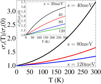
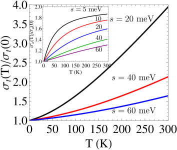
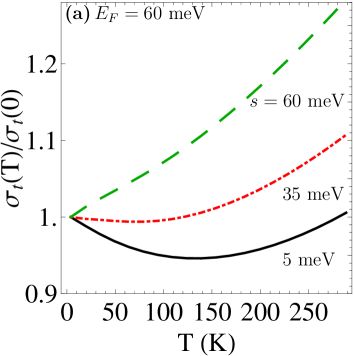
where the temperature dependence of has been given in Eq. (8). The total conductivity due to the activation behavior approaches a limiting value and all temperature dependence comes from the thermal excitation through the change of the effective carrier density in the presence of the inhomogeneity given in Eq. (8). Thus at very high temperatures () the MLG conductivity at the charge neutral point increases quadratically regardless of the sample quality. In Fig. 3 the temperature dependent conductivity has been calculated at charge neutral point, where the temperature dependent scattering mechanism can be neglected. In Ref. [Heo et al., 2011], about 60% increase of conductivity is observed as the temperature increases from 4 K to 300 K. We estimate the potential fluctuation parameter meV for this sample based on our theoretical analysis as compared with the data.
III.2 of MLG at finite doping ()
At finite doping () the temperature dependent conductivities are very complex because three energies (, , and ) are competing among them. Especially when , regardless of , we have the asymptotic behavior of conductivities in region 1 and 2 from Eqs. (29) and (30), respectively,
| (36a) | |||||
| (36b) | |||||
where and . The leading order correction is linear but the coefficient is exponentially suppressed by the term . This fact indicates that in the high mobility sample with small , the activated conductivity is weakly temperature dependent except at low density regimes, i.e. . Since the density increase by thermal excitation is also suppressed exponentially by the same factor [see Eq. (25)], the dominant temperature dependent conductivity arises from the scattering time Das Sarma et al. (2011), which manifests the metallic behavior. On the other hand, for a low mobility sample with a large , the linear temperature dependence due to thermal activation can be observed even at high carrier densities .
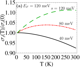
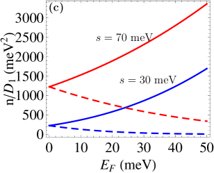
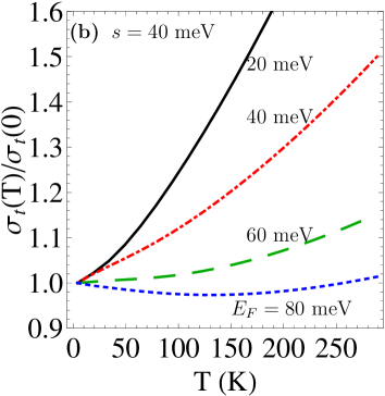
In Fig. 4 we present the total conductivities of inhomogeneous MLG as a function of temperature (a) for a fixed Fermi energy and several and (b) for a fixed and several Fermi energies. The calculations for Fig. 4 are all carried out for MLG on SiO2 substrate (corresponding to dielectric constant ), charged impurity density cm-2 and short-ranged disorder strength (eV Å)2. For total conductivity, the thermally activated insulting behavior competes with the temperature-dependent screening effects, where the latter always give the metallic behavior in conductivity for MLG samples. When is small, the activated behavior is suppressed and the total conductivity shows the metallic behavior. While for large value of , i.e., the low mobility sample, the thermal activation overwhelms the metallic temperature dependence and the system manifests insulating behavior. For the situation becomes much complex. At low temperatures, the leading order of the temperature dependence is linear (the second term in Eq. (36)) and the total conductivity starts at weakly insulating behavior. As the temperature increases, the screening effects begin to dominant leading to the metallic behavior. As a result, the temperature evolution of the conductivity becomes non-monotonic and for large (or low mobility samples) the nonmonotonic behavior can be more pronounced as shown in experiments Heo et al. (2011).
IV Temperature dependent carrier density of inhomogeneous BLG
In the following of this paper, we extend our previous studyHwang and Das Sarma (2010) on the insulating behavior in metallic bilayer graphene and compare it with MLG situation. The most important difference between MLG and BLG comes from the fact that, in the BLG, the two layers are weakly coupled by interlayer tunneling, leading to an approximately parabolic band dispersion with an effective mass about ( corresponds to the bare electron mass) contrast to linear-dispersion Dirac carrier system for MLG. As done for MLG, we assume the electronic potential fluctuations in BLG system to be a Gaussian form given in Eq. 1 and this potential is felt equally by both layersAbergel et al. (2011).
In the presence of potential fluctuations the density of states (DOS) for disordered BLG is given by , where is the DOS in a homogeneous BLG system, where and are the spin and valley degeneracies, respectively. We have cm-2/meV assuming . The DOS of hole can be calculated from the following relation: . In Fig. 5, the density of states of both electron and hole are shown for the inhomogeneous BLG system. In the presence of potential fluctuations, the electron and hole coexist for certain amount of regions near CNP and their DOS approach to the homogeneous case as the carrier energy further increases.
Because BLG is also a gapless semiconductor like MLG, the direct thermal excitation from valence band to conduction band at finite temperatures composes an important source of temperature dependent transport in BLG. Thus, the temperature dependence of thermally excited electron density is first to be considered.
IV.1 of BLG at CNP ()
With the help of Eq. 6, we could get the total electron density for BLG in the presence of electron-hole puddles. We first consider the situation at CNP, where all electrons are located in the band tail at and the electron density in the band tail is given by Abergel et al. (2011). Contrast to the quadratic dependence of in MLG, the electron density in the band tail for BLG is linearly proportional to the standard deviation . Unlike MLG, which has the exact formula for (i.e., Eq. (8)), we could only find the asymptotic behavior of at finite temperatures for BLG. The low temperature () behavior of electron density at CNP becomes
| (37) |
Thus, the electron density increases quadratically at low temperature limit. For homogeneous BLG with the constant DOS the electron density at finite temperatures is given by , which has the universal slope . The presence of the band tail suppresses the thermal excitation of electrons and gives rise to the quadratic behavior. However, at high temperature limit, the density increases linearly with the same slope approaching to the homogeneous system, i.e.,
| (38) |
In Fig. 6(a) we show the temperature dependent electron density at CNP for different standard deviations. Compared with the inset of Fig. 3, it is apparent that, even for the same strength of potential fluctuation , the effects of thermal excitation of carrier density are much stronger in BLG than in MLG sample, which leads to more easily observed insulating behavior in BLG samples.
IV.2 of BLG at finite doping ()
In this subsection, we derived the total electron density at finite temperatures for inhomogeneous BLG away from CNP. Contrary to MLG, we need to calculate the finite temperature chemical potential (i.e., Eqs. 13 and 20). The charge conservation relation in both homogeneous and inhomogeneous BLG gives the temperature independent chemical potential , allowing us to directly calculate the total effective electron (hole) density. In the case of finite gate voltage, i.e., , the electron density of the homogeneous BLG for is given by
| (39) |
where and . The thermal excitation is exponentially suppressed due to the Fermi function at low temperatures (). While at high temperatures () it increases linearly. In the presence of finite potential fluctuations (), the electron and hole density at zero temperature for the inhomogeneous system are given by:
| (40) |
where and the difference of electron and hole density () is independent of the strength of potential fluctuation (see Fig. 6(c)). At low temperatures () the asymptotic behavior of the electron density is given by
| (41) |
The leading order quadratic behavior of as in undoped BLG () is strongly suppressed by potential fluctuation. For the situation , the existence of electron-hole puddles gives rise to a notable quadratic behavior [see Fig. 6(b)]. At high temperatures () we find
| (42) |
where the linear temperature dependence of electron density is dominant as the homogeneous system.
V conductivity of inhomogeneous BLG
With the help of total electron and hole density calculated above, we will derive the temperature dependent conductivity for BLG in the presence of electron-hole puddles. We will apply both Boltzmann theoryDas Sarma et al. (2010) and effective medium theoryKirkpatrick (1973) to interpret the intriguingly insulating behavior observed in BLG samplesZhu et al. (2009); Feldman et al. (2009); Nam et al. (2010).
The density and temperature dependent average conductivities in BLG, denote as and , are given within the Boltzmann transport theory:
| (43) |
where and are average electron and hole densities, respectively. is the transport relaxation time for bilayer graphene:
| (44) |
and is calculated with Eq. 28. But for BLG systems, one needs to use the parabolic dispersion relation for the pseudo-spin state “” and the static dielectric screening function derived in Ref. [Hwang and Das Sarma, 2008b]. The wave function form factor associated with the chiral nature of BLG is also different from the case in MLG, which is given by . To determine the average scattering time in BLG, we take into account the long-range charged impurity scattering and short-range defect scattering, which has been established that both contribute significantly to bilayer graphene transport propertiesDas Sarma et al. (2010). The activated conductivities should also be included in the presence of density inhomogeneity in the BLG, which follow the same relation as given for MLG :
| (45a) | |||||
| (45b) | |||||
V.1 of BLG at CNP
When electron-hole puddles form in the BLG samples (denote the electron (hole) puddle as region ‘1’ (‘2’)), the transport properties can be treated with effective medium theory as described in Sec. III. And Eqs. 29-33 for the inhomogeneous MLG also apply to the inhomogeneous BLG system. We will first discuss the total conductivity of BLG at CNP (). In this case, the electron and hole are equally occupied and the total conductivity (see Eq. 32a and 33). At low temperature limit (), the activated conductivities increase linearly with a slope as the temperature increases. The next order temperature correction to the conductivity is quadratic , which arises from the thermal activation (see Eq. 37). Thus, at low temperature limit the total conductivity at CNP is given by
| (46) |
At high temperatures (), the total conductivity is given by:
| (47) |
It is apparent that the activation behavior approaches a limiting value at high temperature limit () while the thermally activated electron density becomes dominant, which increases linearly with a universal slope regardless of the sample quality. Thus, all temperature dependence of the total conductivity comes from the thermal excitation through the change of the carrier density given in Eq. (38). In Fig. 7 we show the calculated temperature dependent conductivity at charge neutral point. The inset present the activated conductivity versus the temperature. In Ref. [Zhu et al., 2009], at the CNP of the BLG sample increases almost two times as temperature varies from 4 K to 300 K. Our theoretical analysis using a potential fluctuation parameter meV gives reasonable agreement with the experimental data.
V.2 of BLG at finite doping ()
The temperature dependent conductivities at finite doping () are very complex because three energies (, , and ) are competing. Regardless of , when , we have the asymptotic behavior of conductivities in region 1 and 2 the same as MLG situation, given in Eq. (36). But the average electron and hole conductivities ( and ) are quite different from MLG case, which is determined by the specific band dispersion relation and also the dielectric function . Thus, the leading order correction to in BLG is also linear, which comes from the activated conductivity, but the coefficient is exponentially suppressed by the term . In the high mobility sample with small , the activated conductivity is weakly temperature dependent except around CNP, i.e. . Since the density increase by thermal excitation is also suppressed exponentially by the same factor [see Eq. (41)] the dominant temperature dependent conductivity arises from the scattering mechanismDas Sarma et al. (2011). On the other hand, in the low mobility sample with large value of , the linear temperature dependence due to thermal activation can be observed even at high carrier densities .
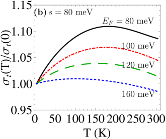
In Fig. 8 we calculate the total conductivities (a) for a fixed and several and (b) for a fixed and several . Even for homogeneous BLG, there are two scattering mechanism competing with each other. The short-range disorder in BLG contributes to a strong insulating transport behavior for all temperature, whereas screened Coulomb scattering always leads to a metallic behavior for Das Sarma et al. (2010). At low temperature limit, the total conductivity decreases with increasing temperature, but at higher temperatures, the short-range disorder contribution becomes quite big and leads to a increasing with . Therefore, when is small, the scattering mechanism is dominant and the total conductivity manifests a non-monotonic temperature dependence (see Fig. 8(a)). However, for large the activated temperature dependence behavior overwhelms the metallic temperature dependence, and the system shows insulating behavior (see Fig. 8(b)). It clearly shows that the insulating behavior in BLG sample appeared at carrier densities as high as cm-2 or higher.
VI Connection to earlier theories
We have demonstrated theoretically that the observed insulating behavior in temperature-dependent monolayer and bilayer graphene conductivity can be explained by the thermal activation between puddles. There are also other theories which have been elaborated to explain low carrier density graphene transport Adam et al. (2007); Rossi et al. (2009); Das Sarma et al. (2010). In this section, we establish the bridge to connect our current theory and earlier theories on graphene transport due to the formation of inhomogeneous electron-hole puddles near the charge neutrality point.
The key qualitative difference between our theory and all earlier graphene transport theories is the introduction of the 2-component transport model where regular diffusive metallic carrier transport coexists with local activated transport due to activation across potential fluctuations in the puddles. Our theory just explicitly accounts for the inhomogeneous landscape in the system, which earlier theories ignored. This 2-component nature of graphene transport, where both metallic and insulating behavior coexist because of the existence of puddles, produces the experimentally observed complex temperature dependence with the low-density behavior being primarily insulating-like and the high-density behavior being primarily metallic-like.
Two different theories have been developed to study the low-density transport in graphene, where the strong density inhomogeneity is dominated. In Ref. [Adam et al., 2007] Adam et al. qualitatively explained the plateau-like approximate nonuniversal minimum conductivity at low carrier density observed in monolayer graphene samples. The basic idea is to introduce an approximate pinning of the carrier density at at low carrier density limits , where is an impurity density. The constant minimum conductivity is then given by for . This simple theory for monolayer graphene transport qualitatively explained the existence of conductivity minimum plateau and the extent to which the minimum conductivity is not universal, which was in good agreement with the observed density-dependent conductivity over a wide range of charged impurity densitiesTan et al. (2007a); Chen et al. (2008a). However, this theory did not take account of the highly heterogeneous structure near charge neutrality point and the thermally activated conductivity at finite temperatures, which then can not explain the observed non-monotonic temperature dependent transport in low mobility graphene samplesHeo et al. (2011).
A more elaborate Thomas-Fermi-Dirac (TFD) theory and an effective medium approximation (EMT) have been introduced in Refs. [Rossi and Das Sarma, 2008] and [Rossi et al., 2009] to study the electrical transport properties of disordered monolayer graphene. The ground state-density landscape can be obtained within this TFD approach and the resultant electrical transport can be calculated by averaging over disorder realizations and the effective medium theory. This theory gives a finite minimum conductivity and is able to explain the crossover of the density-dependent conductivity from the minimum value at the Dirac point to its linear behavior at higher doping. Later, this TFD-EMT theory is also applied to calculate the conductivity of disordered bilayer graphene in Ref. [Das Sarma et al., 2010]. The TFD-EMT technique successfully explains the graphene, both MLG and BLG, transport properties in the theoretically difficult inhomogeneity-dominant regime near the charge neutral point, but this approach fails to explain the temperature dependence of the conductivity for a wide range of temperatures.
In our current model discussed above, we include three effects, the electron-hole structure formation, the thermal activated conductivities and the temperature dependence of screening effects, to explain the temperature-dependent conductivity in both monolayer and bilayer graphene systems. The nonmonotonic temperature-dependent conductivity in graphene systems is then naturally understood from the competition between the thermal activation of charge carriers and the temperature-dependent screening effects. Our transport theory qualitatively explains the observed coexisting metallic and insulating transport behavior in both MLG and BLG systems. For low mobility MLG samples, the dominant role on graphene conductivity switches from the thermally activated transport of inhomogeneous electron-hole puddles to metallic temperature-dependent screening effects, which gives rise to a nonmonotonic behavior from the strong insulating behavior at low temperatures to metallic behavior at high temperatures. On the other hand, another nonmonotonic temperature-dependent transport can be observed in very high mobility bilayer graphene devices, i.e., from metallic behavior at low temperatures due to the screening effects of Coulomb scattering to insulating behavior at high temperatures due to the short-range disorder. The merit of our model is that it is so simple that we could get the asymptotic behavior at low and high temperature limits analytically. Moreover, it provides a clear physical picture of the dominant mechanisms at different regimes as discussed above.
VII Discussions and Conclusions
We first discuss the similarity and the difference between MLG and BLG transport from the perspective of our transport-theory considerations. We find that both manifest an insulating behavior in for low mobility samples. We also find that both systems could exhibit a non-monotonic temperature dependent conductivity for low mobility samples. However, the physical origin for the non-monotonic temperature dependence is quite different in the two systems: in the MLG the non-monotonic feature comes from the competition between thermal activation and the metallic screening effects, which leads to first increasing and then decreasing with increasing temperature (see Fig. 4(a)). While for BLG, the competition between short-range insulating scattering and metallic Coulomb screening effects leads to first decreasing and then increasing as temperature increases (see Fig. 8(a)). Most important quantitative difference between MLG and BLG transport comes from their band dispersions, which leads to much weaker effects of density inhomogeneity in MLG so that the anomalous insulating temperature dependence of is typically not observed in MLG away from the CNP although the gate voltage dependence of MLG and BLG conductivities are similarMorozov et al. (2008); Xiao et al. (2010). The linear Dirac carrier system for MLG leads to linear DOS, which goes to zero at CNP, but the parabolic band dispersion relation in BLG leads to a constant DOS. Due to the difference in the density of states between homogeneous MLG and BLG, the modified DOS in inhomogeneous MLG is increased (see Fig. 1) rather than decreased in inhomogeneous BLG (see Fig. 5). The dimensionless potential fluctuation strength () is much weaker in MLG than in BLG from simple estimates: where , and upto cm-2. Direct calculations Das Sarma et al. (2011) show that the self-consistent values of tend to be much larger in BLG than in MLG for identical impurity disorder. In addition, the qualitatively different DOS leads to much stronger effective short-range scattering in BLG compared with MLG even for the same bare scattering strength. Thus, the insulating behavior in will show up at high temperatures even for relatively higher mobility BLG samples (i.e., small ). In contrast, only in very low mobility MLG samples, where is very large, can the insulating behavior of temperature dependent resistivity be observedTan et al. (2007b); Heo et al. (2011). No simple picture would apply to a gapped () BLG system, since four distinct energy scales (, and ) will compete and the conceivable temperature dependence depends on their relative valuesCastro et al. (2007); Oostinga et al. (2008); Mak et al. (2009). Our assumption of BLG quadratic band dispersion is valid only at low ( cm-2) carrier densities, where most of the current transport experiments are carried out. At higher densities the band dispersion is effectively linear and the disorder effects on are weaker.
Before concluding, we emphasize that our theory is physically motivated since puddles are experimental facts in all graphene samples. Puddles automatically imply a 2-component nature of transport since both diffusive carriers and activated carriers can, in principle, contribute to transport in the presence of puddles. Of course, the effect of puddles is much stronger at low carrier densities, explaining why insulating (metallic) temperature dependence is more generic at low (high) graphene carrier densities. We emphasize that local carrier activation in puddles is just one of (at least) four different independent transport mechanisms contributing to the temperature dependent conductivity. The other three are temperature dependent screening (Ref. [Hwang and Das Sarma, 2009]), phonons (Refs. [Hwang and Das Sarma, 2008a; Min et al., 2011]), and Fermi surface thermal averaging (Refs. [Hwang and Das Sarma, 2009; Müller et al., 2009]). Our theory presented here includes the three electronic mechanisms for temperature dependence: screening, Fermi surface averaging, and puddle activation. We leave out phonons, which have been considered elsewhere (Ref. [Hwang and Das Sarma, 2008a; Min et al., 2011]) and will simply add to the temperature dependent resistivity. The weak phonon contribution to graphene resistivity makes it possible for the electronic mechanisms to dominate even at room temperatures, but obviously at high enough temperatures, the system will, except perhaps at the lowest densities around the CNP, manifest metallic temperature dependence with the resistivity increasing with temperature because of phonon scattering. Similarly, the puddle effects dominate low densities and therefore, the insulating behavior will persist to very high temperatures around the zero-density CNP since activation across potential fluctuations are dominant at the CNP. It is gratifying to note that these are precisely the experimental observations. We note that in general the temperature dependent conductivity of graphene could be very complex since many distinct mechanisms could in principle contribute to the temperature dependence depending on the carrier density, temperature range, and disorder in the system. Inclusion of phonons (at high temperatures) and quantum localization (at low temperatures) effects, which are both neglected in our theory, can only complicate things further. What we have shown in this work is that the low-density conductivity near the CNP is preferentially dominated by density inhomogeneity and thermal carrier activation effects leading to an insulating temperature dependence in the conductivity whereas the high-density conductivity, where the puddles are screened out, is dominated by a metallic conductivity due to temperature-dependent screening effects. This general conclusion is consistent with all experimental observations in both MLG and BLG systems to the best of our knowledge except at very high temperatures where phonon effects would eventually lead to metallic behavior at all densities.
To conclude, we have investigated both MLG and BLG transport in the presence of electron-hole puddles within an analytic statistical theory. Our theory explains the experimentally measured insulating behavior at low temperatures and the consequent nonmonotonic behavior for low mobility samples Heo et al. (2011); Nam et al. (2010); Zou and Zhu (2010). A reasonable quantitative agreement with the experimental data can be obtained by choosing appropriate disorder parameters in our theory (i.e. potential fluctuation and impurity strength) for different samples. We find that the puddle parameter , defining typical potential fluctuations, to be around meV in typical graphene samples as extracted by fitting our theory to existing experimental transport data near the charge neutrality point. These values of potential fluctuations characterizing the graphene charge neutrality point are very consistent with direct numerical calculations of graphene electronic structure in the presence of quenched charged impuritiesDas Sarma et al. (2011); Rossi et al. (2009); Rossi and Das Sarma (2008); Das Sarma et al. (2010). We also relate our current model to earlier theories using the picture of diffusive transport through disorder-induced electron-hole puddles. Finally, we show the similarity and the quantitative difference between MLG and BLG transport in the presence of puddles.
Acknowledgements.
QL acknowledges helpful discussions with D. S. L. Abergel. The work is supported by ONR-MURI, NRI-NSF-SWAN.Appendix A A self-consistent formulation of graphene density of states in the presence of inhomogeneity
Below we provide a microscopic theory to calculate self-consistently the electronic density of states in the presence of the potential fluctuations caused by random charged impurities located near graphene/substrate interface, which has been applied to two dimensional semiconductor based electron gas systemsStern (1976). This self-consistent approach mainly addresses two problems with the presence of random charged impurities. One is the screening of the long-range Coulomb interactions between the carriers and the charged impurities. The other is the real-space potential fluctuations produced by the random array of charged impurities.
The motivation for this appendix is two-fold: (1) providing a microscopic self-consistent theory of graphene density of states in the presence of puddles; (2) showing that our approximate physically-motivated density of states (Eq. 4) is an excellent approximation to the self-consistent density of states.
A.1 Monolayer graphene
First, we apply the self-consistent consideration of random charged impurities on the density of states in monolayer graphene.
The simple theory of linear screening givesStern (1976):
| (48) |
where is the Thomas-Fermi screening wavevector, is the density of states at the Fermi level and is the dielectric constant ( for graphene on SiO2 substrate).
The screening constant shown in Eq. 48 enters Poisson’s equation for the potential change produced by a charge density (associated with the charged impurities in the graphene/substrate environment). For a charge (we use in the calculation) located at and (on top of the graphene layer), the additional Coulomb potential satisfies:
| (49) |
where in the vacuum (), in SiO2 () and . For graphene, is the carrier density distribution normal to the interface and .
To solve Eq. 49 we take advantage of the cylindrical symmetry to writeStern and Howard (1967) :
| (50) |
The potential will satisfy Eq. 49 if
| (51) |
At the interface , must be continuous and satisfy . should also satisfies the boundary condition as . In addition, the impurity potential will go to zero at the metallic contact below the SiO2 (i.e., and is the thickness of the SiO2 layer). Such screening effects are absent in the SiO2. After some algebra, the explicit expression of for insulator thickness and the impurity distance from graphene/substrate interface is given by:
| (52) |
For the thickness of insulator in the limit , we have , which has been given in the Appendix B of Ref. [Stern and Howard, 1967]. The potential fluctuations with an array of point charges at random positions in the plane have a mean-square variation about the average potential Stern (1976):
| (53) |
To obtain specific results for the electronic density of states and the screening constant we use the simple Gaussian broadening approximation for the density of statesArnold (1974). The disorder-induced potential energy fluctuations is described by (Eq. 53). Then the density of states becomes
| (54) |
where erfc is the complementary error function, , , is the graphene (Fermi) velocity, and are the spin and valley degeneracies, respectively.
By choosing the chemical potential as a tuning parameter we have the following coupled equations:
| (55) |
For fixed values of , , and , we get the self consistent results for , by solving the above two coupled equations. The electron density could be gotten from the formula:
| (56) |
where is the Fermi-Dirac distribution function. The electron density in the presence of disorder-induced electron-hole puddles has been discussed in Sec. II, where we use the potential fluctuation as a fixed parameter. And here we self-consistently solve the parameter from a microscopic point of view, which is in good agreement with the results shown in Sec. II. The potential fluctuation in Eq. 53 affects the electronic density of states. But the fluctuations depend on the screening via Eq. 51 while the screening depends on the density of states via Eq. 48. Therefore, we have a coupled problem which must be solved self-consistently.
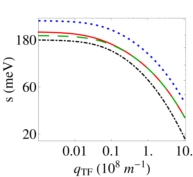
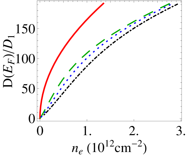
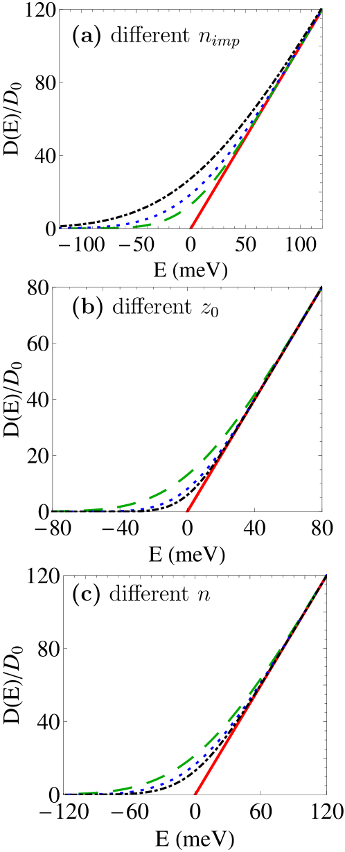
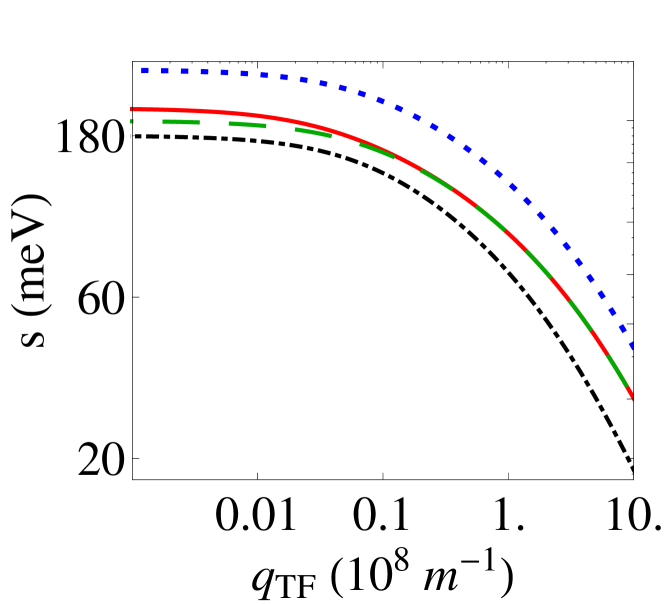
In Fig. 9, the standard deviation of the potential fluctuation and the screening constant are plotted for different values of the Fermi level. The self-consistently solved parameters depend on the fixed charged impurity density , the SiO2 thickness , the location of the fixed charged impurity , and the Fermi level (i.e. the carrier density ). All these four effects can be understood from physical intuition. The reduction of the SiO2 thickness weakens the potential fluctuations when the screening length is small even though there is a little effect for strong screening. As the charged impurities go away from the graphene layer the potential fluctuations is also reduced, while the potential fluctuations becomes stronger with the higher impurity density. Increasing the carrier density gives rise to the stronger screening effects, and leads to weaker potential fluctuations.
In Fig. 10, the density of states of monolayer graphene is given with the parameters of SiO2 thickness nm and the distance of fixed charged impurities nm for different impurity densities . In Fig. 11, we present the electronic density of states for different carrier densities and impurity configurations. The self-consistent calculation of the density of states verifies the results presented in Sec.II as shown in Fig. 1, where we choose the potential fluctuation as an adjustable parameter. For monolayer graphene, the presence of spatially random charged impurities increases the electronic density of states in the whole range of energy. The corresponding hole density of states can be obtained by changing the sign of energy .
A.2 Bilayer graphene
In this subsection, we provide the density of states in bilayer graphene in the presence of potential fluctuations. As shown for monolayer graphene, we use the linear screening written asStern (1976):
| (57) |
where is the density of states of BLG at the Fermi level and is the dielectric constant and for BLG on SiO2, .
Following the same procedure discussed for MLG, the disorder-induced potential fluctuation is described by the Gaussian form and the corresponding density of states can be written as (also see Sec. IV):
| (58) |
where erfc is the complementary error function, (as given in Eq. 53), , and are the spin and valley degeneracies, respectively. The main difference between MLG and BLG is in their density of states of non-interacting systems. The homogeneous MLG system has the linear energy-dependent density of states while the density of states of the homogeneous BLG is independent of energy, which leads to different Thomas-Fermi screening wavevectors. The potential fluctuation in Eq. 53 affects the electronic density of states in BLG. But the fluctuations depend on the screening via Eq. 51 while the screening depends on the density of states via Eq. 57. Therefore, we have a coupled problem which must be solved self-consistently.
In Fig. 12, the broadening parameter and the screening constant are plotted for various Fermi levels (i.e. the carrier density ). As shown for MLG, the BLG parameters are also non-trivial function of the fixed charge density , the SiO2 thickness , the location of the fixed charged impurity , and the Fermi level. The different charged impurity configurations and carrier densities have similar effects on potential fluctuations of bilayer graphene as we discussed for monolayer graphene. The results for are also quite similar to that of MLG (in Fig. 9) only with small numerical difference.
In Fig. 13, the self-consistent electronic density of states of BLG has been calculated using SiO2 thickness nm and distance of fixed charged impurities nm for different impurity densities. The higher impurity density changes the density of states more dramatically. In Fig. 14, we show the electronic density of states of BLG for different charged impurity configurations and carrier densities. The existence of random charged impurities reduces the electronic density of states for but create a band tail for .
References
- Das Sarma et al. (2011) S. Das Sarma, S. Adam, E. H. Hwang, and E. Rossi, Rev. Mod. Phys. 83, 407 (2011).
- Castro et al. (2007) E. V. Castro, K. S. Novoselov, S. V. Morozov, N. M. R. Peres, J. M. B. L. dos Santos, J. Nilsson, F. Guinea, A. K. Geim, and A. H. Castro Neto, Phys. Rev. Lett. 99, 216802 (2007).
- Lee et al. (2010) Y. Lee, S. Bae, H. Jang, S. Jang, S.-E. Zhu, S. H. Sim, Y. I. Song, B. H. Hong, and J.-H. Ahn, Nano Letters 10, 490 (2010).
- Novoselov et al. (2005) K. S. Novoselov, D. Jiang, F. Schedin, T. J. Booth, V. V. Khotkevich, S. V. Morozov, and A. K. Geim, Proc. Natl. Acad. Sci. USA 102, 10451 (2005); K. S. Novoselov, A. K. Geim, S. V. Morozov, D. Jiang, M. I. Katsnelson, I. V. Grigorieva, S. V. Dubonos, and A. A. Firsov, Nature 438, 197 (2005).
- Tan et al. (2007a) Y.-W. Tan, Y. Zhang, K. Bolotin, Y. Zhao, S. Adam, E. H. Hwang, S. Das Sarma, H. L. Stormer, and P. Kim, Phys. Rev. Lett. 99, 246803 (2007a).
- Chen et al. (2008a) J. H. Chen, C. Jang, S. Adam, M. Fuhrer, E. D. Williams, and M. Ishigami, Nat. Phys. 4, 377 (2008a).
- Hong et al. (2009) X. Hong, K. Zou, and J. Zhu, Phys. Rev. B 80, 241415 (2009).
- Chen et al. (2009) F. Chen, J. Xia, and N. Tao, Nano Letters 9, 1621 (2009).
- Tan et al. (2007b) Y.-W. Tan, Y. Zhang, H. Stormer, and P. Kim, Eur. Phys. J. Special Top. 148, 15 (2007b).
- Chen et al. (2008b) J. H. Chen, C. Jang, S. Xiao, M. Ishigami, and M. S. Fuhrer, Nat. Nanotechnol. 3, 206 (2008b).
- Hwang and Das Sarma (2009) E. H. Hwang and S. Das Sarma, Phys. Rev. B 79, 165404 (2009).
- Lv and Wan (2010) M. Lv and S. Wan, Phys. Rev. B 81, 195409 (2010).
- Hwang et al. (2007) E. H. Hwang, S. Adam, and S. Das Sarma, Phys. Rev. Lett. 98, 186806 (2007).
- Rossi et al. (2009) E. Rossi, S. Adam, and S. Das Sarma, Phys. Rev. B 79, 245423 (2009).
- Martin et al. (2008) J. Martin, N. Akerman, G. Ulbricht, T.Lohmann, J. H. Smet, K. V. Klitzing, and A.Yacoby, Nat. Phys. 4, 144 (2008).
- Zhang et al. (2011) Y. Zhang, V. W. Brar, C. Girit, A. Zettl, and M. F. Crommie, Nat. Phys. 5, 722 (2009); A. Deshpande, W. Bao, F. Miao, C. N. Lau, and B. J. LeRoy, Phys. Rev. B 79, 205411 (2009); A. Deshpande, W. Bao, Z. Zhao, C. N. Lau, and B. J. LeRoy, Phys. Rev. B 83, 155409 (2011).
- Heo et al. (2011) J. Heo, H. J. Chung, S.-H. Lee, H. Yang, D. H. Seo, J. K. Shin, U.-I. Chung, S. Seo, E. H. Hwang, and S. Das Sarma, Phys. Rev. B 84, 035421 (2011).
- Zhu et al. (2009) W. Zhu, V. Perebeinos, M. Freitag, and P. Avouris, Phys. Rev. B 80, 235402 (2009).
- Feldman et al. (2009) B. Feldman, J. Martin, and A. Yacoby, Nat. Phys. 5, 889 (2009).
- Zou and Zhu (2010) K. Zou and J. Zhu, Phys. Rev. B 82, 081407 (2010).
- Nam et al. (2010) S.-G. Nam, D.-K. Ki, and H.-J. Lee, Phys. Rev. B 82, 245416 (2010).
- Hwang and Das Sarma (2008a) E. H. Hwang and S. Das Sarma, Phys. Rev. B 77, 115449 (2008a).
- Min et al. (2011) H. Min, E. H. Hwang, and S. Das Sarma, Phys. Rev. B 83, 161404 (2011).
- Hwang and Das Sarma (2010) E. H. Hwang and S. Das Sarma, Phys. Rev. B 82, 081409 (2010).
- Abergel et al. (2011) D. S. L. Abergel, E. H. Hwang, and S. Das Sarma, Phys. Rev. B 83, 085429 (2011).
- Rossi and Das Sarma (2008) E. Rossi and S. Das Sarma, Phys. Rev. Lett. 101, 166803 (2008).
- Arnold (1974) E. Arnold, Appl. Phys. Lett. 25, 705 (1974).
- San-Jose et al. (2007) P. San-Jose, E. Prada, and D. S. Golubev, Phys. Rev. B 76, 195445 (2007); J. H. Bardarson, J. Tworzydło, P. W. Brouwer and C. W. J. Beenakker, Phys. Rev. Lett. 99, 106801 (2007); E. Louis, J. A. Vergés, F. Guinea, and G. Chiappe, Phys. Rev. B 75, 085440 (2007).
- Zallen and Scher (1971) R. Zallen and H. Scher, Phys. Rev. B 4, 4471 (1971).
- Eggarter and Cohen (1970) T. P. Eggarter and M. H. Cohen, Phys. Rev. Lett. 25, 807 (1970).
- Du et al. (2008) X. Du, I. Skachko, A. Barker, and E. Y. Andrei, Nature Nanotech. 3, 491 (2008).
- Bolotin et al. (2008) K. I. Bolotin, K. J. Sikes, J. Hone, H. L. Stormer, and P. Kim, Phys. Rev. Lett. 101, 096802 (2008).
- Müller et al. (2009) M. Müller, M. Bräuninger, and B. Trauzettel, Phys. Rev. Lett. 103, 196801 (2009).
- Kirkpatrick (1973) S. Kirkpatrick, Rev. Mod. Phys. 45, 574 (1973).
- Das Sarma et al. (2010) S. Das Sarma, E. H. Hwang, and E. Rossi, Phys. Rev. B 81, 161407 (2010).
- Hwang and Das Sarma (2007) E. H. Hwang and S. Das Sarma, Phys. Rev. B 75, 205418 (2007).
- Ferreira et al. (2011) A. Ferreira, J. Viana-Gomes, J. Nilsson, E. R. Mucciolo, N. M. R. Peres, and A. H. Castro Neto, Phys. Rev. B 83, 165402 (2011).
- Hwang and Das Sarma (2008b) E. H. Hwang and S. Das Sarma, Phys. Rev. Lett. 101, 156802 (2008b).
- Adam et al. (2007) S. Adam, E. H. Hwang, V. M. Galitski, and S. Das Sarma, Proc. Natl. Acad. Sci. USA 104, 18392 (2007).
- Morozov et al. (2008) S. V. Morozov, K. S. Novoselov, M. I. Katsnelson, F. Schedin, D. C. Elias, J. A. Jaszczak, and A. K. Geim, Phys. Rev. Lett. 100, 016602 (2008).
- Xiao et al. (2010) S. Xiao, J.-H. Chen, S. Adam, E. D. Williams, and M. S. Fuhrer, Phys. Rev. B 82, 041406 (2010).
- Oostinga et al. (2008) J. B. Oostinga, H. B. Heersche, X. Liu, A. F. Morpurgo, and L. M. K. Vandersypen, Nat. Mater. 7, 151 (2008).
- Mak et al. (2009) K. F. Mak, C. H. Lui, J. Shan, and T. F. Heinz, Phys. Rev. Lett. 102, 256405 (2009).
- Stern (1976) F. Stern, Surface Science 58, 162 (1976).
- Stern and Howard (1967) F. Stern and W. E. Howard, Phys. Rev. 163, 816 (1967).