Stone-Wales–type transformations in carbon nanostructures driven by electron irradiation
Abstract
Observations of topological defects associated with Stone-Wales–type transformations (i.e., bond rotations) in high resolution transmission electron microscopy (HRTEM) images of carbon nanostructures are at odds with the equilibrium thermodynamics of these systems. Here, by combining aberration-corrected HRTEM experiments and atomistic simulations, we show that such defects can be formed by single electron impacts, and remarkably, at electron energies below the threshold for atomic displacements. We further study the mechanisms of irradiation-driven bond rotations, and explain why electron irradiation at moderate electron energies (100 keV) tends to amorphize rather than perforate graphene. We also show via simulations that Stone-Wales defects can appear in curved graphitic structures due to incomplete recombination of irradiation-induced Frenkel defects, similar to formation of Wigner-type defects in silicon.
pacs:
68.37.Og, 81.05.ue, 64.70.Nd, 31.15.esI Introduction
Stone-Wales defect Thrower69 ; Stone1986 – (55-77) – is the simplest example of topological disorder in graphene and other -hybridized carbon systems. It can be formed by rotating a C-C bond by with regard to the midpoint of the bond – referred to as the SW transformation – so that four hexagons are turned into two pentagons and two heptagons. This defect has received considerable amount of attention Ma2009a ; Ertekin2009 ; Zhou2003 ; Li2005 ; Miyamoto2004 ; Suenaga2007 , because it has the lowest formation energy among all intrinsic defects in graphenic systems, and because it presumably plays an important role in plastic deformation of carbon nanotubes (CNT) under tension Huang2006 by relieving strain Nardelli1998 . It can also act as a source for dislocation dipoles Ertekin2009 ; Ding2007 .
Regardless of being the lowest energy defect in graphene Banhart2011 and other -hybridized carbon nanostructures, the (55-77) needs about 5 eV to appear in graphene Ma2009a ; Li2005 , and 3–5 eV in CNTs with a diameter above 1 nm Ertekin2009 ; Zhou2003 , which should lead to a negligible equilibrium concentration of such defects at room temperature. However, recent advances in HRTEM have allowed the identification of such defects in graphene Meyer2008 ; Kotakoski2011 and CNTs Suenaga2007 . Moreover, SW transformations play an important role in the response of graphene to electron irradiation Kotakoski2011 ; Song2011 , leading to changes in the morphology of vacancy-type defects Lee2005b and to their migration. Such changes are equally surprising, because the barrier for bond rotation is about 5 eV Li2005 ; Cretu2010 , which should exclude thermal activation as a cause for SW transformation at room temperature during experimentally relevant time scales. Regarding irradiation effects, previous simulations Yazyev2007 showed that an energy of eV must be transferred to a C atom in graphene in the in-plane direction for a bond rotation to occur. Also this cannot explain the frequently observed SW transformations under the usual TEM imaging conditions, since with typical acceleration voltages ( kV) the transferred kinetic energy in the direction almost perpendicular to the electron beam will remain significantly below 10 eV.
Here, by combining aberration-corrected (AC-) HRTEM with atomistic computer simulations, we show that topological defects associated with the SW transformation can be formed in -hybridized carbon nanostructures by impacts of individual electrons at energies even below the threshold for a carbon atom displacement. We further study in detail the mechanisms of irradiation-driven bond rotations for pre-existing vacancy-type defect structures and how they transform and migrate due to electron impacts. At the same time we explain why electron irradiation at moderate energies ( keV) tends to rather amorphize Kotakoski2011 than perforate graphene. We also show via simulations that the (55-77) can appear in curved graphitic structures due to “incomplete” recombination of irradiation-induced Frenkel defects, reminiscent of the formation of Wigner-type defects in silicon Tang1997 .
II Methods
II.1 Experimental Methods
Graphene membranes used in our experiments were prepared by mechanical exfoliation of graphite on Si/SiO2 substrates and transfer of the resulting graphene sheets onto TEM grids as described previously Meyer2008a . For TEM experiments we used an FEI Titan equipped with an image-side aberration corrector, operated at 80 kV. The spherical aberration was set to 15 m and images were recorded at Scherzer defocus. The extraction voltage of the source was reduced to 2 kV and the condensor lens C2 was switched off in order to minimize the energy spread. Under these conditions, dark contrast in the images can be directly interpreted in terms of the atomic structure. Image sequences were recorded on a CCD camera with exposure times of 1 s and intervals of approximately 2 s.
II.2 Computational Methods
We carried out atomistic computer simulations based on the spin-polarized density functional theory (DFT) implemented in the plane wave basis set vasp code Kresse1996 . The projector augmented wave potentials Blochl1994 were used to describe the core electrons, and the generalized gradient approximation of Perdew, Burke and Ernzernhof Perdew1996 for exchange and correlation. We included plane waves up to a kinetic energy of 300 eV. The -point sampling of the Brillouin zone was performed using the scheme of Monkhorst-Pack Monkhorst1976 for the periodic dimensions. Structure relaxation calculations were combined with molecular dynamics (DFT-MD) simulations with a lower kinetic energy threshold and fewer -points.
Due to the high computational cost of the DFT-MD method, only a few simulations were carried out at this level. Whenever statistics needed to be gathered, we calculated the forces using the non-orthogonal DFT-based tight binding (DFTB) method Frauenheim2002 . The main results were checked against DFT-MD. In total, we carried out dynamical DFTB-MD simulations. The simulated structures consisted of 120–200 atoms and were fully optimized. For the displacement threshold simulations, one of the atoms was assigned a kinetic energy with the initial velocity vector pointing to a preselected direction. The initial temperature of the system was set to 5 K, although we observed no differences when carrying out the simulations for initially stationary atoms. Displacement threshold (minimum kinetic energy required to eject the atom) was found to be 22.50 eV, in a good agreement with earlier DFTB results Krasheninnikov2005b ; Zobelli2007a . It is also close to the DFT value (22.03 eV) Kotakoski2010 . For the annihilation simulations, various system temperatures were studied (500–1200 K) both to fasten the migration of the adatoms and to understand the effect of an elevated temperature (as will be mentioned below).
III Results and Discussion
III.1 Stone-Wales Defects due to Single Electron Impacts
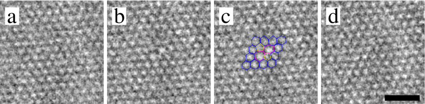
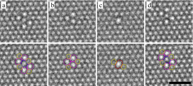
We begin the presentation of our results with the description of experimental observations of (55-77) in HRTEM images. Several long image sequences, typically containing hundreds of images from clean and initially defect-free graphene membranes, were recorded at 80 kV. Occasionally, (55-77) defects appear in individual exposures, as in the example shown in Figure 1b (Figure 1c with structure overlay). Remarkably, in most of the observed cases, isolated (55-77) appeared in pristine graphene for one 1 s exposure, only to disappear in the following frame. Hence, the lifetime of this defect under the 80 kV electron beam in terms of irradiation dose is of the order of , the dose used for a single exposure.
To understand the appearance and disappearance of (55-77) , we carried out atomistic simulations for individual displacement events under the electron beam. After calculating , we extended this calculation to all in-plane () and out-of-plane angles in the range , Figure 2. Displacements with would result in transferred kinetic energies of more than 2 eV below for an electron beam even at 120 keV. Since the displacement threshold increases for increasing , it is unlikely that this restriction would lead us to miss any significant electron beam-induced structural changes, especially for electron energies similar to those used in this study (80 keV). The calculated displacement thresholds are shown in Figure 2 in a relative scale along with the space angles for which we observed the formation of (55-77) .
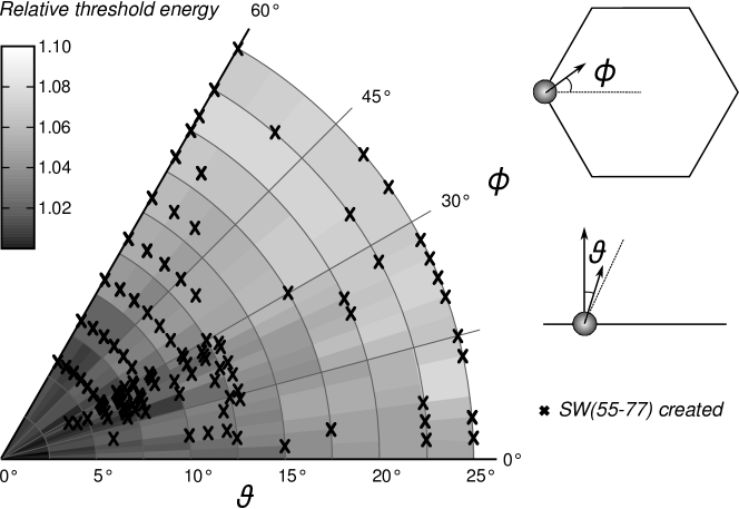
It is evident from Figure 2 that the SW transformation is a very likely event at displacement angles slightly away from the graphene plane normal (). The transferred kinetic energies () required for this process are below the displacement threshold for the corresponding and () since no actual removal of the recoil atom is required for the bond rotation to occur. Typically, eV resulted in the (55-77) formation, although for some space angles even eV was enough. The probability for (55-77) formation is particularly high for certain space angles, which is related to different mechanisms of SW transformation, as described below.
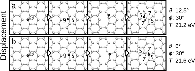
The above-presented result is in clear contrast with the earlier simulation results for graphite Yazyev2007 where no (55-77) formation was observed for low . This discrepancy is caused by the neighboring graphene planes in the case of graphite: The displaced atom gets attached to the adjacent layer and does not therefore initiate a bond rotation. In Figure 3 we show the two processes which account for the majority of the SW transformations observed during our simulations. In the “circle” process (Figure 3a), the displaced atom circles around its neighbor, whereas in the “nudge” process (Figure 3b) it nudges the neighbor to cause the bond rotation. Note that the example cases are for the same and almost same , but for different . The resulting process for each displacement is an interplay of all three variables (, , ).
Similar mechanisms also exist for CNTs. However, as two new parameters (tube diameter and chirality) should be introduced for quantitative analysis of SW transformation, we did not study this process in nanotubes at length due to unreasonably high computational cost.
III.2 Annihilation of Vacancies and Adatoms with Possible Formation of (55-77)
Since we frequently observed formation of vacancy–adatom pairs (adatoms play the role of interstitials in graphene and CNTs) in our simulations of electron impacts onto graphene and earlier in CNTs Krasheninnikov2005b , we also explored another possible mechanism of (55-77) formation, which is based on “incomplete” annihilation of a Frenkel defect. This study was motivated by the peculiarities of the recombination of such a defect in bulk silicon. In that covalently-bonded material the recombination can give rise to either annihilation of the defect and restoration of the perfect crystal lattice, or to a Wigner-type defect Tang1997 . Such topological defects are imperfections in the crystal lattice with the locally “correct” number of atoms (as opposed to vacancies and interstitials), with the atomic configuration separated from the perfect structure by a finite potential barrier. Such defects are deemed to also exist in graphite Ewels2003 ; Telling2003 , and (55-77) can clearly be classified into this group.
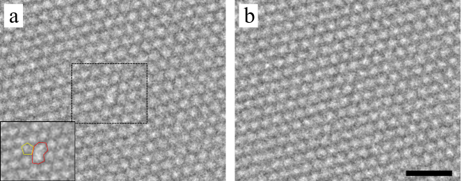
While carbon adatoms on graphene Lehtinen2003 ; Erni2010 and CNTs Gan2008 ; Krasheninnikov2006 (especially those inside nanotubes) are mobile at room temperature, they can easily find vacancies in the system and annihilate. Indeed, we occasionally observed disappearance of vacancies in HRTEM image sequences. Figure 4 shows an example of a mono-vacancy that disappears during observation. This proves that mobile carbon atoms are present under our experimental conditions, and may recombine with vacancy-type defects. However, we never noticed the creation of a (55-77) after an observed mono-vacancy.
To simulate the annihilation process, we created nearby Frenkel defects (separated by a few Ångströms) in a graphene layer and small (6,6) zigzag and (10,0) armchair CNTs (radii Å and Å, respectively). We then heated the structures and collected statistics on the evolution of each system by running dynamical atomistic simulations at various temperatures (500–1200 K). Three possible outcomes emerged from the simulations: (1) perfect annihilation to the pristine structure (similar to the experimental images in Figure 4), (2) formation of a (55-77) (Figure 5a) and, surprisingly, (3) sputtering of a C2 dimer with a remaining reconstructed di-vacancy (5-8-5) (Figure 5b).
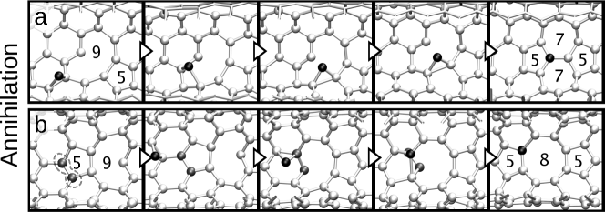
For graphene, we always observed perfect annihilation in accordance with the experiments. However, if the adatom in graphene was placed on top of one of those two bonds in the nine-membered carbon ring which are right next to the pentagon, a (55-77) was spontaneously formed without an energy barrier. Thus (55-77) may also form in graphene due to recombination of Frenkel defects, but the probability for this process must be much lower than in CNTs.
For (10,0) CNT, we obtained perfect annihilation in approximately 54% of cases, (55-77) was formed in approximately 34% of cases and dimer sputtering occurred in approximately 12% of cases. For (6,6) CNT, the values were 53%, 42% and 4%, respectively. With increasing temperature the probability to sputter a dimer showed a slight tendency to increase. We also ran the calculations for a (8,8) CNT ( Å) at 800 K in order to estimate the curvature dependency of the results. The values did not significantly differ from those for the (6,6) CNT, except for a somewhat increased tendency to perfect annihilation and decreased sputtering (with probabilities of 56% and 2%, respectively).
The formation energy of a spatially separated Frenkel defect in graphene within the DFTB model is approximately 11.1 eV. Transformation to form SW defect from this initial setup leads to an energy gain of 5.4 eV. By sputtering a dimer, graphene would instead gain 0.4 eV. Hence, all three observed outcomes are energetically reasonable also for graphene. For nanotubes, the formation energies of both (55-77) and a di-vacancy are lowered due to the curvature and stronger C-C bonds at pentagons Krasheninnikov2006 . The corresponding energy gains are also higher, which can explain why the probability for (55-77) defect formation and dimer evolution is higher in curved carbon nanostructures. The actual energies depend on the local curvature. It is also plausible that the dimer evaporation process plays a role in shrinking fullerenes under electron irradiation Huang2007 .
III.3 Stone-Wales Transformations in Vacancy-Type Defects
(55-77) defect represents the elementary case of a topological change in the graphene structure, i.e., a single bond rotation in the otherwise perfect structure. More abundant, however, are changes in the atomic configuration through bond rotations in the reconstructed vacancy defects, as recent experiments indicate Kotakoski2011 ; Song2011 . In presence of a (multi-)vacancy, the atomic configuration of a defect can be transformed between different metastable structures via bond rotations. It was presumed Kotakoski2011 that such SW transformations of vacancy-type defects would be stimulated by electron impacts, but the actual atomistic mechanism has not been hitherto unraveled.
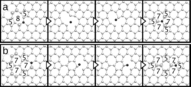
In order to get microscopic insight into irradiation-stimulated bond rotations near vacancy-type defects in graphene, we carried out a set of experiments and dedicated simulations aimed at assessing the probability of SW transformations in the defect structures. In our experiments, we initially generated “defective” graphene by brief 150 kV electron irradiation, and then recorded image sequences of di-vacancies using 80 kV AC-HRTEM. As observed previously Kotakoski2011 , the vacancies can transform between different configurations under the influence of the 80 kV electron beam. Moreover, the di-vacancies migrate and transition between the different reconstructed configurations via SW transformations, typically until they cluster into larger defects (see videos S5 and S6 in Ref. Suppl ).
In Figure 6, we show an example of a di-vacancy defect that transforms between different reconstructed shapes [(5-8-5), (555-777), (5555-6-7777)] under the electron beam. The changes in the atomic structure of these di-vacancy configurations can be described by SW transformations at the defect. Moreover, multiple transformations allow migration of the di-vacancy. Similar to (55-77) defect formation discussed above, the activation energy for these transitions is far too high to allow a thermally activated process with an observable rate at room temperature. Hence, on the basis of the observations, the activation energy for the transition must be provided by the electron beam.
In order to confirm that the SW transformations at these defects are caused by single electron impacts, we carried out atomistic simulations of such impacts onto atoms near di-vacancies. Due to the computational cost related to many non-equivalent atoms present in the system and a large number of possible atomic configurations, we could not repeat the detailed analysis of the role of initial space angle of the displacement similar to pristine graphene, and therefore limited our simulations to the case for all non-equivalent atoms at reconstructed di-vacancy structures. However, because the defects break the symmetry of the lattice, a directional preference for the displacements arises (atom displaced in the perpendicular direction will change its direction due to local strain). This effect is strong enough to facilitate bond rotations in reconstructed di-vacancy structures. In Figure 7 we present examples of such processes for both (5-8-5)(555-777) and (555-777)(5555-6-7777) transformations.
Within these simulations, we never observed (555-777)(5-8-5) transformations. Because the symmetry of the (555-777) defect around the middle atom is the same as that of pristine graphene (the middle atom is represented as a black sphere in the last panel of Figure 7a), one would also expect that a displacement is required for this transformation, similar to the (55-77) case, although in principle the surrounding atoms could also cause this transformation. We noticed that the most likely di-vacancy transformation, at least for , is the (5555-6-7777)(555-777). The (5-8-5)(555-777) was the least likely one of those observed. We never observed a (5-8-5)(5-7) transformation Kotakoski2011 during our simulations, which we also attribute to the limited simulated conditions (). Curiously, however, we did observe one transformation in which a (5-8-5) di-vacancy directly migrated one step in the zigzag lattice direction.
Another interesting observation originating from these simulations is the fact that the displacement threshold for atoms in the central part of the reconstructed defects [(555-777) and (5555-6-7777)] are higher than that for pristine graphene (by as much as 5%). This may explain why defect structures tend to grow into larger and larger amorphous patches instead of collapsing into holes under continuous electron irradiation at low voltages ( keV) Kotakoski2011 : Even when atoms are removed from the defected area, the displacements occur at the edges of the existing defects rather than at the central part where the local atomic density is already lower. Clearly, since the core structure of these defects consists of carbon hexagons, there must exist a limiting size above which the displacement threshold becomes similar to that of ideal graphene.
IV Conclusions
To conclude, by combining AC-HRTEM experiments and atomistic simulations, we have shown that the bond rotations which lead to creation of topological defects in carbon nanostructures are caused by single electron impacts or incomplete annihilation of Frenkel defects. This explains the discrepancy between experimental observations of Stone-Wales defects and their relatively high formation energy and even higher energy barrier for bond rotation.
The SW transformation in graphene can be initiated at least in two different ways upon electron impact (involving a “circling” or “nudging” motion), and for almost any space angle, provided that enough energy is transferred from the electron to the target atom. Our simulations indicate that (55-77) can appear as a result of “incomplete” recombination of a Frenkel defect reminiscent of the formation of Wigner-type defects in silicon Tang1997 . However, this is much more likely in the case of local curvature, as in nanotubes. More surprisingly, we also observed sputtering of C2 dimer as a result of annihilation of a Frenkel defect in carbon structures with high curvature.
Moreover, we showed that the displacement threshold of atoms in the central area of reconstructed defects is higher than that of pristine graphene, by as much as 5%, which explains why defected graphene under low-energy electron irradiation ( keV) tends to turn graphene into a two-dimensional amorphous structure Kotakoski2011 instead of a perforated membrane. For different di-vacancy structures, even displacements in direction perpendicular to the graphene layer can initiate SW transformation and thus local structural changes and defect migration.
Our results provide microscopic insight into the irradiation-induced changes in the atomic structure of carbon nanosystems under electron irradiation, and taking into account the interesting electronic properties of defects associated with SW transformations Kotakoski2011 ; Lherbier2011 ; Appelhans2010 , may open new avenues for irradiation-mediated engineering Krasheninnikov2010 of carbon nanostructures with next-generation electron microscopes.
V Acknowledgments
We acknowledge financial support by the German Research Foundation (DFG), the German Ministry of Science, Research and Arts (MWK) of the state Baden-Wuerttemberg within the SALVE (sub angstrom low voltage electron microscopy) project and Academy of Finland through several projects. We also thank CSC, Espoo, Finland, for generous grants on computer time.
References
- (1) Thrower, P. The study of defects in graphite by transmission electron microscopy. In Chemistry and physics of carbon, vol. 5; Edited by P. L. Walker Jr., Marcel Dekker: New York, 1969.
- (2) A. J. Stone and D. J. Wales, Chem. Phys. Lett. 128, 501 (1986).
- (3) J. Ma, D. Alfé, A. Michaelides, E. Wang, Phys. Rev. B 80, 033407 (2009).
- (4) E. Ertekin, D. C. Chrzan, and M. S. Daw, Phys. Rev. B 79, 155421 (2009).
- (5) L. G. Zhou and S. Shi, Appl. Phys. Lett. 83, 1222 (2003).
- (6) L. Li, S. Reich, and J. Robertson, Phys. Rev. B 72, 184109 (2005).
- (7) Y. Miyamoto, A. Rubio, S. Berber, M. Yoon, and D. Tománek, Phys. Rev. B 69, 121413+ (2004).
- (8) K. Suenaga, H. Wakabayashi, M. Koshino, Y. Sato, K. Urita, and S. Iijima, Nat. Nanotech. 2, 358 (2007).
- (9) J. Y. Huang, S. Chen, Z. Q. Wang, K. Kempa, Y. M. Wang, S. H. Jo, G. Chen, M. S. Dresselhaus, and Z. F. Ren, Nature 439, 281 (2006).
- (10) M. B. Buogiorno Nardelli, B. I. Yakobson, and J. Bernholc, Phys. Rev. B 57, R4277 (1998).
- (11) F. Ding, K. Jiao, M. Wu, and B. I. Yakobson, Phys. Rev. Lett. 98, 075503+ (2007).
- (12) F. Banhart, J. Kotakoski, and A. V. Krasheninnikov, ACS Nano 5, 26 (2011).
- (13) J. C. Meyer, C. Kisielowski, R. Erni, M. D. Rossell, M. F. Crommie, and A. Zettl, Nano Letters 8, 3582 (2008).
- (14) J. Kotakoski, A. V. Krasheninnikov, U. Kaiser, and J. C. Meyer, Phys. Rev. Lett. 106, 105505+ (2011).
- (15) B. Song, G. F. Schneider, Q. Xu, G. Pandraud, C. Dekker, and H. Zandbergen, (2011).
- (16) G. D. Lee, C. Z. Wang, E. Yoon, N. M. Hwang, D. Y. Kim, and K. M. Ho, Phys. Rev. Lett. 95, 205501 (2005).
- (17) O. Cretu, A. V. Krasheninnikov, J. A. Rodríguez-Manzo, L. Sun, R. M. Nieminen, and F. Banhart, Phys. Rev. Lett. 105, 196102+ (2010).
- (18) O. V. Yazyev, I. Tavernelli, U. Rothlisberger, and L. Helm, Phys. Rev. B 75, 115418 (2007).
- (19) M. Tang, L. Colombo, J. Zhu, and T. Diaz de la Rubia, Phys. Rev. B 55, 14279 (1997).
- (20) J. C. Meyer, C. O. Girit, M. F. Crommie, and A. Zettl, Appl. Phys. Lett. 92, 123110 (2008).
- (21) G. Kresse and J. Furthmüller, Phys. Rev. B 54, 11169 (1996).
- (22) P. E. Blöchl, Phys. Rev. B 50, 17953 (1994).
- (23) J. P. Perdew, K. Burke, and M. Ernzerhof, Phys. Rev. Lett. 77, 3865 (1996).
- (24) H. J. Monkhorst and J. D. Pack, Phys. Rev. B 13, 5188 (1976).
- (25) T. Frauenheim, G. Seifert, M. Elstner, T. Nichaus, C. Köhler, M. Amkreutz, M. Sternberg, Z. Hajnal, A. Di Carlo, and S. Suhai, J. Phys.: Condens. Matter 14, 3015 (2002).
- (26) A. V. Krasheninnikov, F. Banhart, J. X. Li, A. S. Foster, and R. M. Nieminen, Phys. Rev. B 72, 125428 (2005).
- (27) A. Zobelli, A. Gloter, C. P. Ewels, G. Seifert, and C. Colliex, Phys. Rev. B 75, 245402 (2007).
- (28) J. Kotakoski, C. H. Jin, O. Lehtinen, K. Suenaga, and A. V. Krasheninnikov, Phys. Rev. B 82, 113404 (2010).
- (29) See EPAPS Document No. to-be-inserted for experimental videos and additional images. For more information on EPAPS, see http://www.aip.org/pubservs/epaps.html..
- (30) C. P. Ewels, R. H. Telling, A. A. El-Barbary, M. I. Heggie, and P. R. Briddon, Phys. Rev. Lett. 91, 025505 (2003).
- (31) R. H. Telling, C. P. Ewels, A. A. El-Barbary, and M. I. Heggie, Nat. Mater. 2, 333 (2003).
- (32) P. O. Lehtinen, A. S. Foster, A. Ayuela, A. V. Krasheninnikov, K. Nordlund, and R. M. Nieminen, Phys. Rev. Lett. 91, 017202 (2003).
- (33) R. Erni, M. D. Rossell, M. T. Nguyen, S. Blankenburg, D. Passerone, P. Hartel, N. Alem, K. Erickson, W. Gannett, and A. Zettl, Phys. Rev. B 82, 165443+ (2010).
- (34) Y. Gan, J. Kotakoski, A. V. Krasheninnikov, K. Nordlund, and F. Banhart, New J. Phys. 10, 023022 (2008).
- (35) A. V. Krasheninnikov, P. O. Lehtinen, A. S. Foster, and R. M. Nieminen, Chem. Phys. Lett. 418, 132 (2006).
- (36) J. Y. Huang, F. Ding, K. Jiao, and B. I. Yakobson, Phys. Rev. Lett. 99, 175503 (2007).
- (37) A. Lherbier, Simon M.-M. Dubois, X. Declerck, S. Roche, Y. M. Niquet, and J. C. Charlier, Phys. Rev. Lett. 106, 046803 (2011).
- (38) D. J. Appelhans, L. D. Carr, and M. T. Lusk, New Journal of Physics 12, 125006 (2010).
- (39) A. V. Krasheninnikov and K. Nordlund, J. Appl. Phys. 107, 071301 (2010).