Spin accumulation created electrically in an -type germanium channel using Schottky tunnel contacts
Abstract
Using high-quality Fe3Si/-Ge Schottky-tunnel-barrier contacts, we study spin accumulation in an -type germanium (-Ge) channel. In the three- or two-terminal voltage measurements with low bias current conditions at 50 K, Hanle-effect signals are clearly detected only at a forward-biased contact. These are reliable evidence for electrical detection of the spin accumulation created in the -Ge channel. The estimated spin lifetime in -Ge at 50 K is one order of magnitude shorter than those in -Si reported recently. The magnitude of the spin signals cannot be explained by the commonly used spin diffusion model. We discuss a possible origin of the difference between experimental data and theoretical values.
For overcoming the scaling limit of silicon (Si) complementary metal oxide semiconductor (CMOS) devices,Antoniadis germanium (Ge) channels with high electron and hole mobility have been expected.Tezuka ; Lee ; Miyao In general, there are two critical issues for source-drain technologies of Ge-metal-oxide-semiconductor field effect transistors (MOSFETs), i.e., the strong Fermi-level pinning (FLP) at the metal/Ge interfaceDimoulas ; Toriumi and low solubility of the dopants.Chui ; Ikeda Some solutions for the two issues have so far been proposed.Nishimura ; Zhou ; Thathachary ; Yamane ; Sawano Recently, we individually addressed them by fabricating an atomically controlled metal/Ge interfaceYamane and forming an ultrashallow contact with the Sb -doping.Sawano
If the Ge technologies for the high performance MOSFETs are combined with spintronic ones for the nonvolatile memory, one can realize a next-generation CMOS technology with ultra-low-power consumption.Wolf ; Zutic To date, spin-polarized electrons created by an optical method were detected electrically in Ge-based heterostructures.Shen Very recently, electrical spin injection and detection in a Ge channel were also demonstrated in lateral devices with ferromagnet (Fe)-insulator (MgO or AlO) contacts.Zhou1 ; Saito ; Jain ; Jeon Since the insulating barriers for source and drain contacts can result in large parasitic resistance unfortunately, a technique without the insulating barrier for the spin injection and detection in Ge will be required in the scaled MOSFET structures.
In this paper, we show reliable evidence for the detection of spin accumulation created electrically in an -Ge channel through Fe3Si/-Ge Schottky -tunnel-barrier contacts. This is the first step of research and development of Ge-based spintronic devices without using insulating tunnel contacts.
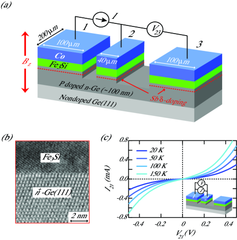
Fe3Si epitaxial films with a thickness of 10 nm were grown on Ge(111) by low-temperature molecular beam epitaxy (MBE) at 130 ∘C.Hamaya Prior to the growth, we fabricated a phosphorus-doped -Ge(111) channel (1018 cm-3) with a thickness of 100 nm on non-doped Ge(111) substrates ( 40 cm) by using an ion implantation technique and an annealing at 600 ∘C.nGe After the fabrication of the -Ge(111) channel, the -Ge(111) layer consisting of a 5-nm-thick Ge epilayer and -doped Sb ( = 1014 cm-2) was grown by MBE.Sawano Conventional processes with photolithography, Ar+ ion milling, and reactive ion etching were used to fabricate a three-terminal lateral device for measurements of the voltage changes induced by a Hanle effect.Lou ; Tran ; Dash ; Sasaki ; Ando ; Dash2 Here a polycrystalline Co layer with a thickness of 25 nm was deposited on the Fe3Si layer by using electron beam evaporation so as to align the magnetic moments in the in-plane direction.
The fabricated device is illustrated schematically in Fig. 1(a). As shown in the cross-sectional transmission electron micrograph of Fig. 1(b), the heterointerface consisting of Fe3Si/-Ge was atomically flat, leading to the reduction in the presence of interface states.Yamane ; Sawano Each contact denoted by 1, 2, or 3 has a lateral dimension of 100 200 m2, 40 200 m2 or 100 200 m2, respectively. The edge-edge distance between contacts 1 and 2 or contacts 2 and 3 was 10 m or 25 m, respectively, and the -Ge(111) layer on the channel region was removed by Ar+ ion milling. The Hanle-effect measurements were performed by a conventional dc method at 50 K. External magnetic fields () for the Hanle-effect measurements were applied perpendicular to the film plane after the magnetic moments of all the contacts were aligned parallel to the film plane.
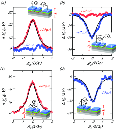
Figure 1(c) shows two-terminal current-voltage () characteristics measured between contacts 1 and 2 for various temperatures. When the sign of is positive, the electrons are injected from the contact 1 into the Ge channel and are extracted from the Ge channel into the contact 2. We can see nonlinear curves for all the temperatures and a weak temperature dependence, indicating that tunneling conduction of electrons through the high-quality Fe3Si/-Ge/-Ge interfaces is dominant. Thus, the asymmetry of the characteristics with respect to the polarity is quite small.
Using this device, we measure the three-terminal voltage, , as a function of at 50 K in the terminal configuration shown in the inset schematic of Fig. 2(a). The red and blue plots show the data for 10 and 10 A, respectively, where a quadratic background voltage depending on is subtracted from the raw data. For 10 A in Fig. 2(a) (red), a voltage change () of 25 V can be seen with increasing from zero to 2 kOe. This is a consequence of the depolarization of spin-polarized electrons, i.e., Hanle-effect curve,Dash ; Lou ; Tran ; Sasaki ; Ando indicating the first experimental detection of spin accumulation created electrically in -Ge using Schottky tunnel contacts. In contrast, for 10 A (blue), we cannot see such voltage changes. This feature means that the presence of the spin accumulation is verified only by a forward-biased contact, i.e., contact 2 in the terminal configuration of Fig. 2(a). When we use the terminal configuration shown in the inset of Fig. 2(b), a voltage change () of 20 V can only be seen for 10 A in Fig. 2(b). This is also evidence for the presence of the spin accumulation in -Ge, detected only by a forward-biased contact, i.e., contact 1. The asymmetric bias dependence can be understood by a difference in the spin-detection sensitivity through the Schottky-tunnel barrier for the spin accumulation in the conduction band of semiconductors, which has already been described by Lou et al. in -GaAs channels.Lou Recently, we also observed the same features in -Si channels.Ando
In addition to the three-terminal methods, Lou et al. confirmed the above bias-dependent detectability by measuring two-terminal Hanle-effect curves in both bias polarities for GaAs-based devices.Lou Following their experiments, we also confirm the two-terminal voltage, , as a function of at 50 K in Figs. 2(c) and 2(d). For 10 A or 10 A, a voltage change () of 25 V or 20 V is observed, respectively. The magnitude of , observed in Figs. 2(c) and 2(d), is almost equal to that shown in Figs. 2(a) and 2(b), respectively. Accordingly, the spin accumulation signals are detected only at the forward-biased contact in such low bias-current region. Considering these facts, we can judge that the spin accumulation created electrically in an -Ge channel is evidently detected using Fe3Si/Ge Schottky tunnel contacts. Here we also tried to measure the inverted Hanle signals, recently reported by Dash et al.Dash2 As a result, we could not see inverted Hanle signals at 50 K. This fact indicates that there is almost no local fluctuation of the magnetic fields at the atomically flat Fe3Si/-Ge/-Ge interface.
A lower limit of spin lifetime () can be estimated from the Hanle-effect signals with a Lorentzian function,Dash () (0)/[1+()2], where / is the Lamor frequency, is the electron -factor ( 1.563),Vrijen is the Bohr magneton. The fitting curves (black solid curves) are shown in Figs. 2 (a), (b), (c), and (d), and the values are roughly estimated to be 125 140 psec at 50 K, which are one order of magnitude shorter than those in Si channels at low temperatures reported recently.Sasaki ; Ando We can infer that the relatively short is arising from the presence of the strong spin-orbit interaction in Ge compared to Si.Hasegawa_Roth
Finally, we discuss the magnitude of (spin signals). For the spin signals with both contacts 1 (100 200 m2) and 2 ( 40 200 m2), we can simply estimate the spin resistance-area-product (spin-) at 50 K, , to be 4.0 104 m2 and 2.0 104 m2, respectively. Using the common diffusion model,Fert we can also calculate the predicted spin signal as ()2/ 61.9 m2, where (1.56 10-3 cm) and ( 0.63 m)cal are resistivity and spin diffusion length of Ge at 50 K, respectively, and (0.10 m) is the thickness of the channel in the fabricated device. As a result, there are large differences (three orders of magnitude) between experimental data and theoretical values. In this context, we discuss two origins as follows. First, we can consider that the actual area associated with the tunneling of electrons is deviated largely from the fabricated contact area, arising from the in-plane inhomogeneous doping density near the interface between Fe3Si and Ge. Actually, the distribution of the heavily doped Sb can become inhomogeneous under the Sb -doping process.Sawano Since the actual area associated to the tunneling conduction was quite small, the difference between the experiment and theory may be quite large. Second, two-step tunneling process via the localized states between Fe3Si and Ge, as proposed by Tran et al.,Tran should be considered. However, we consider that the asymmetric bias dependence shown in Figs. 2 can be explained only by the difference in the spin-detection sensitivity for the spin accumulation in the Ge conduction band, as discussed in detail for Si-based devices.Ando Therefore, we infer that the former is the one of the possible origins of the large difference between experimental data and theoretical values. We should further polish a technique of the Sb -doping processes for fabricating the Schottky-tunnel-barrier contacts.
In summary, we have obtained reliable evidence for the detection of spin accumulation created electrically in an -Ge channel using high-quality Fe3Si/-Ge/-Ge Schottky tunnel contacts in lateral structures. The estimated spin lifetime in -Ge at 50 K was one order of magnitude shorter than those in -Si reported recently. However, the magnitude of the spin signals was deviated largely from the theoretical value based on the spin diffusion model. One of the possible origins of the large deviation is the difference between the actual area associated with the tunneling conduction and the contact area of the fabricated device.
K.H. and M.M. acknowledge Prof. Y. Shiraki, Prof. H. Nakashima, and Prof. T. Kimura for useful discussions. Three of the authors (K.K.,Y.A., and S.Y.) acknowledge JSPS Research Fellowships for Young Scientists. This work was partly supported by Industrial Technology Research Grant Program from NEDO and Grant-in-Aid for Young Scientists (A) from JSPS.
References
References
- (1) D. A. Antoniadis, Proc. Symp. VLSI Technology, 2, (2002).
- (2) T. Tezuka, S. Nakaharai, Y. Moriyama, N. Sugiyama, and S. Takagi, IEEE Electron Device Lett. 26, 243 (2005).
- (3) M. Miyao, K. Toko, T. Tanaka, and T. Sadoh, Appl. Phys. Lett. 95, 022115 (2009).
- (4) C. H. Lee, T. Nishimura, T. Tabata, S. K. Wang, K. Nagashio, K. Kita, and A. Toriumi, IEDM Tech. Dig., 416 (2010).
- (5) A. Dimoulas, P. Tsipas, A. Sotiropoulos, and E. K. Evangelou, Appl. Phys. Lett. 89, 252110 (2006).
- (6) T. Nishimura, K. Kita, and A. Toriumi, Appl. Phys. Lett. 91, 123123 (2007).
- (7) C. O. Chui, K. Gopalakrishnan, P. B. Griffin, J. D. Plummer, and K. C. Saraswat, Appl. Phys. Lett. 83, 3275 (2003).
- (8) K. Ikeda, Y. Tamashita, N. Sugiyama, N. Taoka, and S. Takagi, Appl. Phys. Lett. 88, 152115 (2006).
- (9) T. Nishimura, K. Kita, and A. Toriumi, Appl. Phys. Exp. 1, 051406 (2008).
- (10) Y. Zhou, W. Han, Y. Wang, F. Xiu, J. Zou, R. K. Kawakami, and K. L. Wang, Appl. Phys. Lett. 96, 102103 (2010).
- (11) A. V. Thathachary, K. N. Bhat, N. Bhat, and M. S. Hegde, Appl. Phys. Lett. 96, 152108 (2010).
- (12) K. Yamane, K. Hamaya, Y. Ando, Y. Enomoto, K. Yamamoto, T. Sadoh, and M. Miyao, Appl. Phys. Lett. 96, 162104 (2010).
- (13) K. Sawano, Y. Hoshi, K. Kasahara, K. Yamane, K. Hamaya, M. Miyao, and Y. Shiraki, Appl. Phys. Lett. 97, 162108 (2010).
- (14) S. A. Wolf, D. D. Awschalom, R. A. Buhrman, J. M. Daughton, S. v. Molnár, M. L. Roukes, A. Y. Chtchelkanova, and D. M. Treger, Science 294, 1488 (2001).
- (15) I. Žutic, J. Fabian, and S. D. Sarma, Rev. Mod. Phys. 76, 323 (2004).
- (16) C. Shen, T. Trypiniotis, K. Y. Lee, S. N. Holmes, R. Mansell, M. Husain, V. Shah, X. V. Li, H. Kurebayashi, I. Farrer, C. H. de Groot, D. R. Leadley, G. Bell, E. H. C. Parker, T. Whall, D. A. Ritchie, and C. H. W. Barnes, Appl. Phys. Lett. 97, 162104 (2010).
- (17) Y. Zhou, W. Han, L.-T. Chang, F. Xiu, M. Wang, M. Oehme, I. A. Fischer, J. Schulze, R. K. Kawakami, and K. L. Wang, Phys. Rev. B 84, 125323 (2011).
- (18) H. Saito, S. Watanabe, Y. Minenob, S. Sharma, R. Jansen, S. Yuasa, K. Ando, Solid State. Commun 151, 1159 (2011).
- (19) A. Jain, L. Louahadj, J. Peiro, J. C. Le Breton, C. Vergnaud, A. Barski, C. Beigné, L. Notin, A. Marty, V. Baltz, S. Auffret, E. Augendre, H. Jaffrès, J. M. George, M. Jamet, arXiv:1107.3510v1.
- (20) K. Jeon, B. Min, Y. Jo, H. Lee, I. Shin, C. Park, S. Park and S. Shin, arXiv:1108.3145v1.
- (21) T. Sadoh, M. Kumano, R. Kizuka, K. Ueda, A. Kenjo, and M. Miyao, Appl. Phys. Lett. 89, 182511 (2006); K. Hamaya, Y. Ando, T. Sadoh, and M. Miyao, Jpn. J. Appl. Phys. 50, 010101 (2011); K. Hamaya, T. Murakami, S. Yamada, K. Mibu, and M. Miyao, Phys. Rev. B 83, 144411 (2011).
- (22) C. O. Chui, L. Kulig, J. Moran, W. Tsai, and K. Saraswat, Appl. Phys. Lett. 87, 091909 (2005); A. Satta, T. Janssens, T. Clarysse, E. Simoen, M. Meuris, A. Benedetti, I. Hoflijk, B. De Jaeger, C. Demeurisse, and W. Vandervorstb, J. Vac. Sci. Technol. B 24, 494 (2006).
- (23) X. Lou, C. Adelmann, M. Furis, S. A. Crooker, C. J. Palmstrøm, and P. A. Crowell, Phys. Rev. Lett. 96, 176603 (2006).
- (24) M. Tran, H. Jaffrès, C. Deranlot, J. -M. George, A. Fert, A. Miard, and A. Lemaître, Phys. Rev. Lett. 102, 036601 (2009).
- (25) S. P. Dash, S. Sharma, R. S. Patel, M. P. Jong, and R. Jansen, Nature (London) 462, 491 (2009); S. P. Dash, S. Sharma, J. C. Le Breton, and R. Jansen, Proc. SPIE 7760, 77600J (2010).
- (26) T. Sasaki, T. Oikawa, M. Shiraishi, Y. Suzuki, and K. Noguchi, Appl. Phys. Lett. 98, 012508 (2011).
- (27) Y. Ando, K. Kasahara, K. Yamane, Y. Baba, Y. Maeda, Y. Hoshi, K. Sawano, M. Miyao, and K. Hamaya, Appl. Phys. Lett. 99, 012113 (2011).
- (28) S. P. Dash, S. Sharma, J. C. Le Breton, H. Jaffrès, J. Peiro, J.-M. George, A. Lemaitre, and R. Jansen, Phys. Rev. B 84, 054410 (2011).
- (29) R. Vrijen, E. Yablonovitch, K. Wang, H. W. Jiang, A. Balandin, V. Roychowdhury, T. Mor, and, D. DiVincenzo, Phys. Rev. A 62, 012306 (2000).
- (30) H. Hasegawa, Phys. Rev. 118, 1523 (1960); L. M. Roth, Phys. Rev. 118, 1534 (1960).
- (31) A. Fert and H. Jaffrès, Phys. Rev. B 64, 184420 (2001); A. Fert, J.-M. George, H. Jaffrès, and R. Mattana, IEEE Trans. Electron Devices 54, 921 (2007).
- (32) ( 0.63 m) is calculated by , where is the diffusion constant of our channel at 50 K, 27.7 cm2s-1. For our device, the width () of the contact 1 and 2 is quite lager than .