CALICE Report to the DESY Physics Research Committee
Abstract
We present an overview of the CALICE activities on calorimeter development for a future linear collider. We report on test beam analysis results, the status of prototype development and future plans.
1 Introduction
The CALICE Collaboration pursues the development of highly granular calorimeters for a future e+e- linear collider, based on the particle flow approach for optimal overall detector performance. The Collaboration consists of 57 institutes from 17 countries in Africa, America, Asia and Europe and has about 350 physicists and engineers as members.
We are investigating several technological options for both electromagnetic and hadronic calorimeters. Most of these are candidates for both of the particle flow based ILC detector concepts, ILD and SiD, and for a detector at a multi-TeV linear collider such as CLIC. Our aim is to cover the widest possible range of options with prototypes and to test them using particle beams, thereby maximizing the use of common infrastructure such as mechanical devices, ASIC architecture or DAQ systems. Wherever it is technically feasible and expedient, we work within a common software and analysis framework. This facilitates combination and comparison of test beam data while reducing systematic effects, and allows us to achieve a common understanding of the relative strengths and weaknesses of the options under consideration. This is one of the main strengths of a broadly-based collaboration such as CALICE.
The major part of the effort is focused towards presenting realistic proposals for the detector concept reports of the ILC Technological Design Phase 1, which is due in 2012. This is closely co-ordinated with the detector concept groups. Given the as yet uncertain schedule and energy range that will be required of the future lepton collider, we are also pursuing developments which will only reach a similar level of maturity at a later stage.
The development of calorimeter prototypes generally proceeds in two steps. Physics prototypes provide a proof-of-principle of the viability of a given technology in terms of construction, operation and performance. In addition they are used to collect large data sets for the study of hadronic shower evolution with high granularity. These are invaluable for testing shower simulation programs, and for the development of particle flow reconstruction algorithms with real data.
In contrast, technological prototypes address the issues of scaling, integration and cost optimization. Due to the differing responses of the various active media used to the components of hadronic showers, the physics prototypes are necessary for each combination of active and passive materials under consideration. Technical prototypes are required for each technology, but the effort can be kept to an acceptable level by using common building blocks, and by addressing large area and multi-layer issues separately without instrumenting a full volume.
Synopsis
The completion of data taking with physics prototypes of a silicon based ECAL and scintillator based ECAL and HCAL was reported in 2009. Since then, emphasis has shifted towards analysis of these data, as illustraed by the new results reported here, including detailed comparisons with Geant4- based simulations and a first test of state-of-the art particle flow reconstruction with combined ECAL and HCAL test beam data.
In the meantime, construction of the first gaseous digital HCAL prototype was finished, with front end electronics already integrated in the detector volume. Data taking started in 2010 at the Fermilab test beam facility, using the existing absorber structure and stage. We present first results on detector performance and the status of data taking, which is ongoing in conjunction with the silicon ECAL at the time of this review.
The year 2010 also saw the start o beam tests for a new tungsten HCAL absorber structure, as proposed for the CLIC energy range. Here, the well-understood active scintillator layers are being re-used. We report on a first look into the time structure of the hadronic response in a neutron-rich material.
Major progress was also made with technological prototypes with highly integrated ultra-low power electronics. Final versions of mixed-circuit read-out ASICs were mass-produced and successfully tested, including power-pulsed operation in high magnetic fields. The full read-out chain of the second generation scalable DAQ was established.
The biggest effort here is the construction of an RPC based semi-digital cubic metre scale HCAL prototype for beam tests in 2011, which will establish the electronics integration concept at large scale and contribute to the study of hadronic interactions seen with highly granular gaseous read-out.
Smaller scale technical tests, some ranging up to square-metre sized active layers, were carried out with all considered HCAL read-out technologies, with GEMs, micromegas and scintillator, and are being prepared for the ECAL.
2 Silicon-Tungsten ECAL: SiW
2.1 Introduction
A high granularity ECAL is a central component of a particle-flow optimized detector. It should efficiently identify photons and measure their energy with reasonable precision, and should have excellent capabilities (in conjunction with other subdetectors) to distinguish photonic depositions from those due to other particle types. A sampling calorimeter naturally gives the required granularity in one dimension, while a highly segmented design of the readout layers provides it in the other two dimensions. The choice of tungsten as an absorber material is motivated by its small Molière radius and radiation length and the large difference between its radiation and interaction lengths, ensuring that photonic showers are of small size, and with a significantly different size to hadronic showers. The use of matrices of PIN diodes in high resistivity silicon allows an efficient and low-noise detection of charged particles, and the possibility to efficiently implement highly segmented readout.
2.2 Physics prototype
A first detector prototype, known as the “physics prototype” was constructed during the years 2005–2007. It had an active area of cm2 and 30 sampling layers. It was extensively tested in particle beams between 2006 and 2008 at CERN and FNAL (as seen in Fig. 1). These tests were performed as part of the combined CALICE test beam campaigns with the ECAL followed by a (scintillator-based analogue readout) hadronic calorimeter, and a tail-catcher system, and used beams of electrons, muons and pions with energies between 2 and 180 GeV.
In 2011, the physics prototype will again be placed into test beams at FNAL, this time with a RPC-based digital readout hadronic calorimeter, allowing detailed comparisons between the two HCAL approaches.
The measured performance of this prototype has demonstrated that the silicon tungsten approach can satisfy the various requirements for detector performance at a future lepton collider. The detector has run stably over a period of five years without showing any signs of aging.
2.3 Technological prototype
The focus is now is on the development of the technologies necessary for such a calorimeter to be integrated into a full detector, keeping in mind that large scale, industrialised construction and quality control will be necessary when a final detector is built. Factors considered include a modular design using low power front end electronics integrated into the detector volume, realistic mechanical supporting structures, a compact leak-less cooling system.
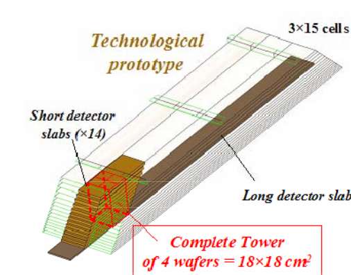
The general design of the module is shown in Fig. 2; details can be found in [1]. The composite-tungsten mechanical structure is a slightly scaled down version of a barrel module envisaged for a linear collider detector, with a length of 1.5 m and a width of around 55 cm, and a total weight of around 600 kg. It has a trapezoidal shape and consists of alveola into which sensitive detector slabs are inserted.
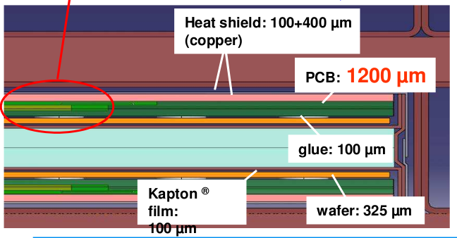
Each detector slab is built around a “H” structure with a tungsten core and composite walls. Both sides of this structure are equipped with active elements consisting of the silicon sensors, a PCB which routes signals and commands between the interior and exterior of the detector, and the front end ASICs embedded into the PCB thickness. A Kapton cable provides the high voltage to the sensors, and a sheet of copper helps to extract the heat to a dedicated heat exchanger at the end of the module. A small Detector InterFace board at the end of each slab is the first element of the common CALICE DAQ system, as described in more detail in Sect. 10
For the technical prototype, a tower with an area of cm2 will be instrumented in all 30 layers, and one long detector slab will be built to test the propagation of signals over long distances within the calorimeter.
2.3.1 Sensors
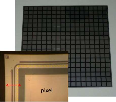
The silicon sensors used in the ECAL are arrays of mm2 PIN diodes made in 300–500m thick high resistivity silicon, and reverse biased at around 200 V. The sensors envisaged for the technical prototype have a total area of cm2. A guard ring structure at the edge of the sensor protects against breakdown. A photograph of such a sensor is shown in Fig. 3.
Current studies include the minimisation of the guard ring region (an effectively dead detector region), and the understanding of the cost drivers for mass production (in close collaboration with industrial partners), with a view to reducing the eventual cost.
Around 40 sensors have already been purchased from HPK, further sensors will have different characteristics: relaxed quality control tolerances (a few dead or noisy channels do not pose a serious problem in reconstruction), more aggressive laser cutting of the wafer to minimise the edge area, and sensors sourced from other manufacturers.
2.3.2 ASIC
A dedicated front end ASIC with 64 channels (SKIROC2) will be used to read the signals from the PIN diodes. It is designed to give a wide dynamic range (from 0.5 to 2500 MIP signals in the sensor), low signal to noise at the single MIP level (around 17 at 1 MIP), and low power consumption, at the level of 25 W/channel (using the power pulsing technique). The schematic of the ASIC is shown in Fig. 4. More than 1000 such chips have been produced, and are in the process of being tested.
2.3.3 PCB
The sensitive layers of the ECAL will be made up of several identical modules, known as Active Sensor Units (ASUs). An ASU is based around a large and thin 8-layer PCB (thickness of around 1 mm, area of cm2) which hosts 16 SKIROC2 ASICs on one side, and on the other side of which are glued the silicon sensors. Signals (both for configuration and data) are routed along lines in the intermediate layers.
Several prototypes of the PCB have been produced, for both packaged and unpackaged ASICs. The main obstacle at present is the planarity of the PCB, particularly for thin models: since rather delicate silicon sensors will be glued to the card, it should not be quite flat. Present prototypes have deviations of several millimetres from perfect planarity over the full area of the card. Modified assembly procedures (temperature/time allowed for cooling) and/or design may result in a flatter PCB, and are under test.
In the case of unpackaged ASICs (as envisaged for the final prototype), the ASICs will be contained within the volume of the PCB, and wire bonded to pads on the PCB. A test of this procedure (results shown in Fig. 5) has already been carried out at the CERN bonding lab. Tests of an epoxy protection layer for the ASICs and wire bonds are underway.
The bias voltage (200 V) will be supplied to the sensors via a flat Kapton cable, prototypes of which have been successfully produced and tested, and a m thick copper layer is used to extract the heat at the end of the slab.
2.3.4 Integration
The task of assembling several ASUs into a detector slab is also under study. The connection between ASUs must be both mechanical and electrical (since signals are routed along the entire length of a detector slab). A previously developed technique involved the deposition of solder paste using a silk-screen and brief heating under a halogen lamp. This technique works well, but is rather labour intensive and requires great care: somewhat impractical for the future industrialisation of the process. A simpler process, based on the use of anisotropic conductive film (ACF), seems to be a very promising alternative. Tests have already been carried out in conjunction with the 3M company, with good results. The main question is whether the fully equipped ASUs can withstand the pressure required to bond the ACF without the fracture of the silicon sensors.
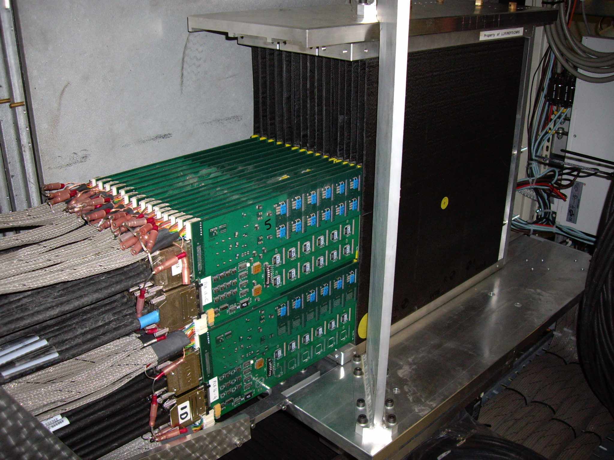
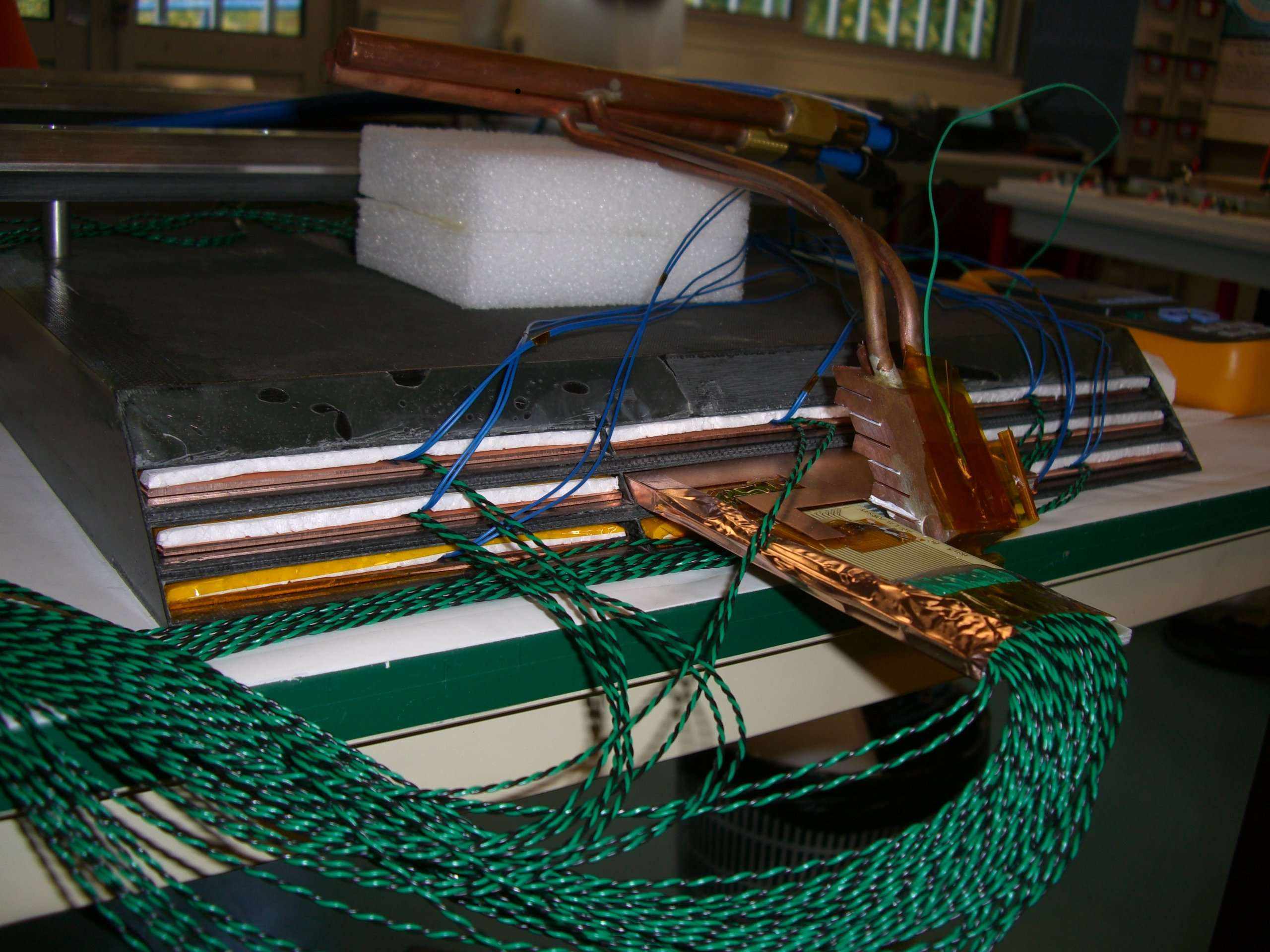
A dedicated assembly laboratory is being prepared at LAL, which will have all necessary equipment to assemble the slabs in a suitable and dedicated environment. A large-scale test of the integration procedure has already been performed for the assembly of the “thermal slabs”, as shown in Fig. 6.
2.3.5 Data acquisition system
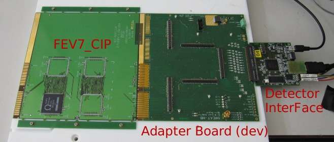
The common CALICE data acquisition system is described in Sect. 10. The integration of the system is continuing, with recent progress including the configuring of the ECAL ASICs via the complete DAQ chain. The various pieces of hardware of the system have been produced, and good progress has been made of the development of the necessary firmware and software. Fig. 7 shows some of the hardware used to test the DAQ chain, with a prototype ECAL ASU (left), an adapter board (centre), and the Detector InterFace card on the right. The full system will be tested using cosmics and particle beams during 2011.
2.3.6 Mechanical structure
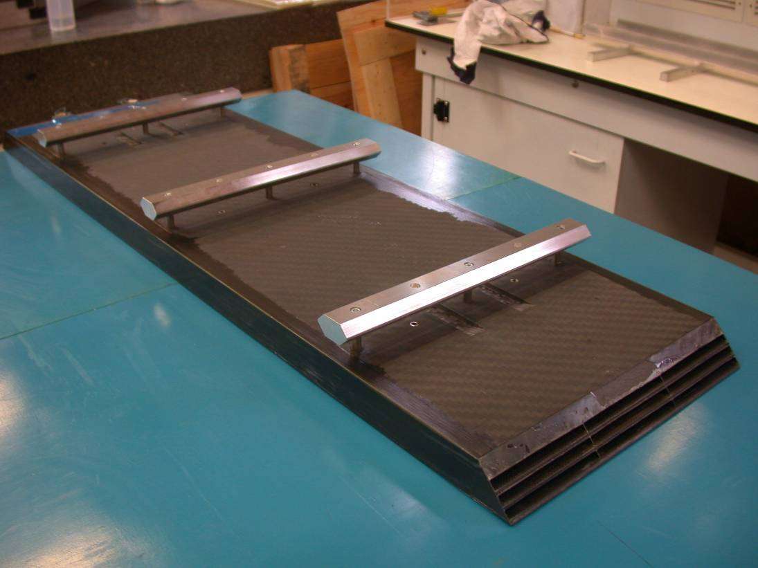
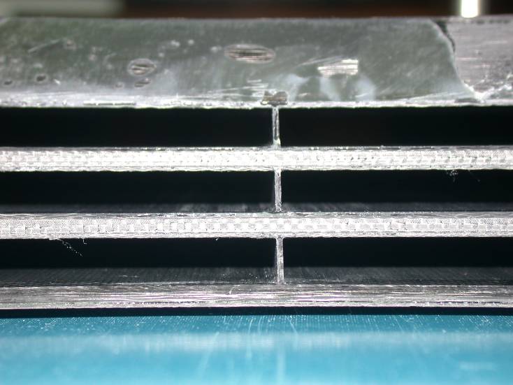
The mechanical supporting structure developed for the technical prototype is close in shape and size to a barrel module envisaged for the barrel part of a linear collider detector (e.g. ILD). It is based on an alveolar structure made in carbon fibre composite material, and incorporates half of the tungsten absorber plates. This allows a modular structure suitable for industrialisation, and minimises the non-instrumented detector regions.
A small “demonstrator” structure, shown in Fig. 8, has already been built to validate the assembly methods and materials. It was produced within the required tolerances.
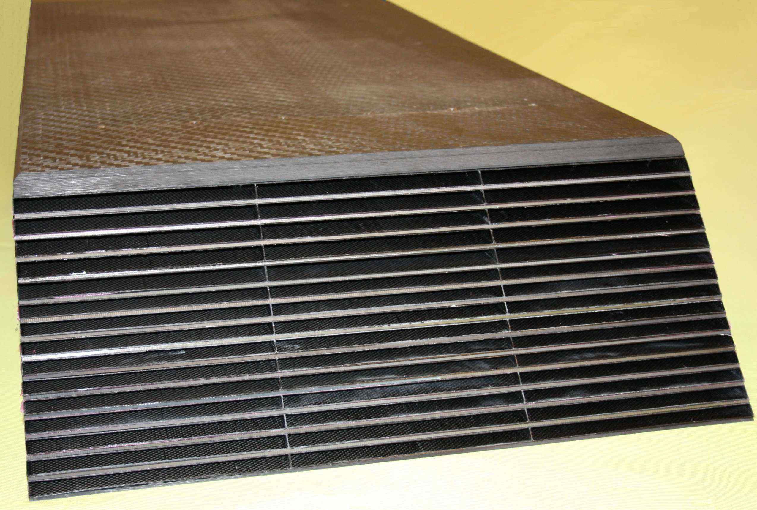
The pieces for the final structure have been produced (as seen in Fig. 9), and an assembly mould has been designed and constructed. Studies to better understand the final thermal curing of the composite are underway in order to ensure successful assembly (there is no possibility to re-do the final curing, so care must be taken!).
The manufacture of the “H” structures is at present on hold, waiting for a definite answer on the feasibility of a sufficiently thin and flat PCB.
The production of longer alveolar structures, required for the endcap detectors (up to 2.5 m long in the current design of ILD) are also under study. The additional length requires extra care to be taken in the manufacture to ensure that the various pieces of the mould can be successfully extracted after the curing of the composite material.
2.3.7 Cooling
The “demonstrator module” has been used to understand the thermal properties of the composite/tungsten alveolar structure. A number of thermal detector slabs have been produced which produce heat at a number of points in a controllable manner, and also measure the temperature. A cooling system has been developed based on cold water circulation. It has been tested and has sufficient performance (with a reasonably generous margin) to cope with the expected power dissipation of the ECAL. This results of the thermal tests have been used to tune thermal simulations of the module’s behaviour, and to apply the same model parameters to simulation of the full technical prototype module and also the entire ECAL system within the ILD detector.
2.4 Future Plans
A first, partially equipped ASU readout using the full CALICE DAQ system will be tested in cosmics and beams during 2011. This will be equipped with a previous version of the ASIC (SPIROC2). Once we are confident that a sufficiently thin and flat PCB can be produced, the “H” structures can be produced. In the case that they cannot, we may proceed with a temporary solution in the short term: a “U” structure holding a single sensitive layer per alveola, which considerably relaxes the constraint on the PCB thickness.
The structure will be gradually equipped, testing various different approaches to the various technical challenges in order to understand their respective strong and weak points.
Once a reasonable number of layers has been produced, they will be tested within the mechanical structure using both cosmic rays and test beams.
3 Scintillator Strip ECAL: ScECAL
3.1 Operational experience with physics prototype
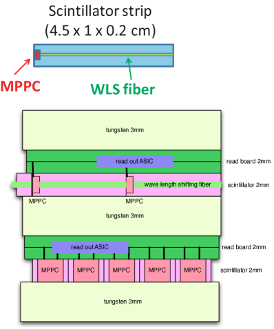
We have constructed and tested two prototypes. Both prototypes use scintillator strips which are 10 mm wide, 45 mm long and 3 mm thick, and wavelength shifting fibres read out by MPPCs, as shown in Fig. 11. The original, smaller prototype was constructed using 18 strips in each of 26 layers, giving a total of 468 strips, while the second prototype has 72 strips in each of 30 layers, giving a total of 2160 strips.
A good energy resolution performance as well as a reasonable linearity was presented in the previous report. For completeness, these results are briefly reported in section 11 below. Those data were taken at the DESY beam test line and FNAL beam test line MT6, in a combined effort from the CALICE Collaboration together with HCAL and tail catcher as well. The successful experience of those beam tests shows that the ScECAL performs well.
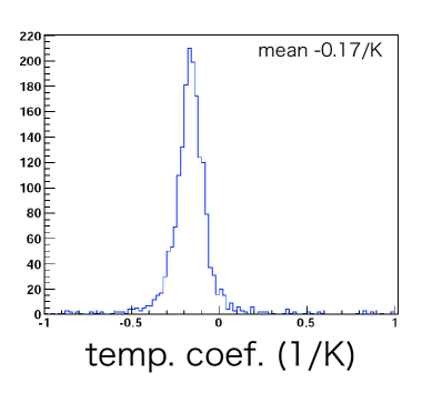
We have installed a calibration system in the prototype at FNAL, which consists of a clear fibre with notches and a LED. Light from the LED passes through a clear fibre and is reflected at the notches along the fibre at the scintillator, then fed into a scintillator strip. The number of lights can be counted and monitored for the stability of the calorimeter system. The temperature coefficients are also extracted at the FNAL beam test and shown in Fig. 12.

3.2 Next generation engineering prototype and current status
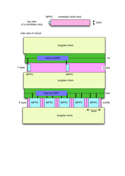
According to the current understanding of PFA studies, a maximum transverse segmentation of 5 mm is favoured, so that we are now aiming to achieve a 5 mm wide strip. The ScECAL incorporating these narrower scintillator strips will be constructed as in Fig. 13.
A prototype should be produced and tested by 2012, according to the plan presented at the previous PRC review.
3.2.1 Strip clustering algorithm development
We have developed algorithms which will allow the energy desposited in the physical scintillator strips to be distributed among (virtual) square cells. This is achieved by making use of the information of the previous and the next layers whose directions are orthogonal to the strip under consideration. This algorithms is called Strip-Splitting and found to work well. One of the results is shown in Fig. 14, where the jet energy resolutions are plotted as a function of the length of the scintillator strip.
3.2.2 Layer electronics development
A few layers are now under construction, as illustrated in Fig. 15. The scintillator layer will be constructed in Korea and Japan. The electronics layer, with SPIROC ASIC from France, is currently being designed by a DESY engineer and will be incorporated into layers in Japan.
3.2.3 5 mm scintillator development
The width of a 5 mm scintillator is expected to be suitable without the use of wave length shifting fibre read out, though homogeneity should be confirmed. This has been tested using collimated 90Sr sources, with preliminary results shown in Fig. 16.
Relatively good uniformity is measured at mm. However, we find non-uniformity due to the acceptance problem in the region near to the photo-sensor. This indicates that further effort is required to achieve optimal response, although in practise the overall energy resolution for electrons and photons are little affected by this non-uniformity.
3.2.4 MPPC development
We now have some MPPCs which consist of 2500 pixels of 20 m2 within a sensitive area of 1 mm1 mm. We have tested these devices and found that the new MPPC exhibits an extended dynamic range, and will continue to characterise their response further.
3.3 Future R&D
The integration of layers of scintillator sensors and readout electronics is the next key issue to be address for the current activity. Since this task is also a combination of several countr (Korea, Germany, France and Japan), international effort for the ILC/ILD will play an important role to achieve it.
4 Digital ECAL: DECAL
4.1 Context
The studies of a digital ECAL (DECAL) continue in the UK, in spite of very significant funding difficulties. In Dec. 2008, the STFC Executive recommended sufficient funding to allow the SPiDER Collaboration to construct a full physics prototype DECAL, as outlined in [2]. By Dec. 2009, the funding for SPiDER had still not been issued and STFC informed the Collaboration that they would not do so.
The UK groups in SPiDER have demonstrated that the INMAPS technology developed specifically for the DECAL application is viable in terms of basic pixel efficiency. INMAPS is implemented as a 0.18 CMOS process in which a deep P-well implant stops signal charge from being absorbed in N-well circuits, and therefore allows the use of both NMOS and PMOS within the pixel, as well as (optionally) high resistivity silicon in the thin epitaxial layer to reduce the charge collection time.
4.2 Testbeams in 2010
Following a successful test beam run at CERN in Sep. 2009 using 120 GeV pions, two further data taking runs have been carried out. The first of these was at DESY in Mar. 2010, for which the primary goal was to quantify the peak electromagnetic shower density observed downstream of specific absorber materials. A secondary goal was to make further pixel efficiency measurements.
Data were recorded with the 1–5 GeV electron beam, using a configuration in which four TPAC 1.2 sensors were aligned precisely along the beam direction using the same custom-built mechanical frame as at CERN. Absorber material (W, Fe, Cu) was placed downstream of these, followed immediately by a further pair of TPAC sensors, to study the shower density. The EUDET telescope was located upstream of the DECAL test stand, as shown in Figure 17.
To complement the DESY run, similar, additional data was recorded at CERN in Sep. 2010, using the EUDET telescope alone as it has finer pitch than the TPAC sensor, with positrons between 10 and 100 GeV. Similar absorber materials and thicknesses to those at DESY were used. Analysis of these data is ongoing, with the aim of having first results to present at TIPP’11 in June.
4.3 Pixel efficiency results
The studies of pixel efficiency from CERN 2009 testbeam and DESY were performed using a set of six TPAC 1.2 sensors aligned along the beam direction, in which the outer four sensors served as a beam telescope, while the two innermost sensors were considered as the devices under test. The trajectory of the beam particle was projected onto the plane of both of these pixels, and each pixel of the test sensors was examined for the presence of hits as a function of the distance from the projected track. The MIP hit efficiency was determined by fitting the distribution of hit probability to a flat top function, convoluted with a gaussion of the appropriate resolution to allow for finite tracking performance. This efficiency, folded for all pixels together, is illustrated in Figure 18.
The MIP efficiency was determined per pixel for both the DESY and CERN data, and for each of the four pixel variants tested. The variants (and corresponding marker colour in Figure 18) are:
-
1.
(red) in 12 standard (non-INMAPS) CMOS;
-
2.
(black) 12 deep P-well CMOS;
-
3.
(green) deep P-well within a 12 high resistivity epitaxial layer;
-
4.
(blue) deep P-well within an 18 high resistivity epitaxial layer.
The results [3] are summarised in Figure 18, for a range of the sensor digital thresholds representative of the signal levels expected in DECAL pixels due to charge spreading. (A typical MIP signal in a 12 epitaxial layer of silicon is 1200 electrons and a single absorbs at most 50% of this due to charge spreading.)
From the results shown in the figure, it is observed that the standard, non-INMAPS sensors have markedly low efficiencies, which is attributed to signal charge being absorbed by in-pixel PMOS transistors. In contrast, the use of the deep P-well reduces the absorption of signal charge by N-wells in the circuitry, improving very substantially the pixel efficiency by a factor of . The addition of the high resistivity epitaxial layer further improves the pixel efficiency to %.
4.4 Future plans
It is no longer an option to plan for a physics prototype DECAL and the short-term future of the DECAL project is extremely uncertain at present. A programme of radiation hardness testing is in progress during 2011, using X-ray sources at RAL, and may be extended to include neutrons and protons. This is in part to understand how the TPAC sensor would satisfy the requirements of SuperB and ALICE ITS. The technology development will continue while this is still possible. The studies which have been carried out so far are in the process of being finalised, and a series of papers, e.g. [4], are in preparation to document what has been achieved.
5 Analogue HCAL Technological Prototype
A technological prototype of a highly granular scintillator based AHCAL is under design and construction to demonstrated the feasibility of this approach in a realistic linear collider (LC) detector. The challenge is the high level of integration to maintain maximum compactness and hermeticity of the final detector, once the AHCAL design is realized as a whole barrel detector for a LC experiment.
The envisaged detector architecture [5, 6] is sketched in Fig. 19. It is inspired by one variant of the ILD detector concept, but is very similar to those envisaged for SiD or CLIC.
The barrel of the AHCAL has a cylindrical structure and will be placed outside the electromagnetic calorimeter, while it is surrounded by the magnet. The cylindrical structure is divided into 16 segments with 48 detector layers each. The figure shows one sector of a barrel subdivided only once along the beam axis. This layout provides access to electronics and service interfaces once the detector end-cap is opened, but poses tight space constraints to the barrel end-cap transition region.
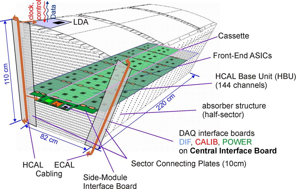
One active layer consists of three parallel slabs. Each slab is again subdivided in six HCAL basic units (HBU) and the middle slab is connected to the DAQ via the Central Interface Board (CIB). The side slabs are in turn connected to the CIB via the Side Interface Boards (SIBs).
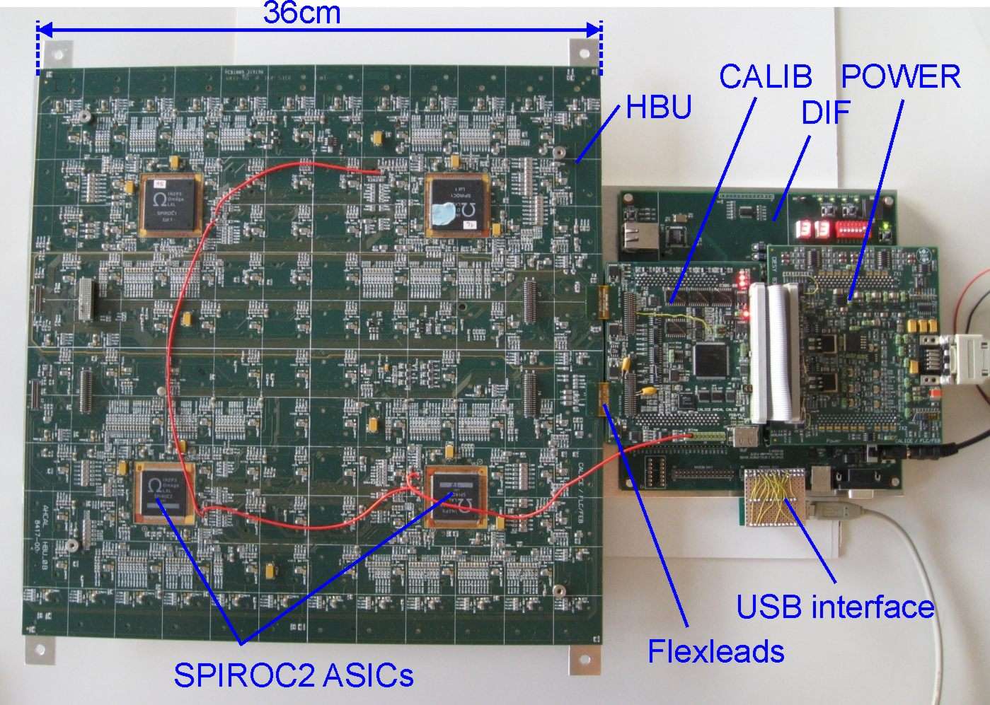
The first HBU module, along with the interface modules, is shown in Fig. 20 left, as it is used in the DESY test setups. In the final design the HBUs are interconnected by flexleads and ultra-thin connectors with a stacking height of 0.8 mm (see Fig. 20 right), which are also used to connect the HBUs to the CIB.
5.1 Tiles and ASICs
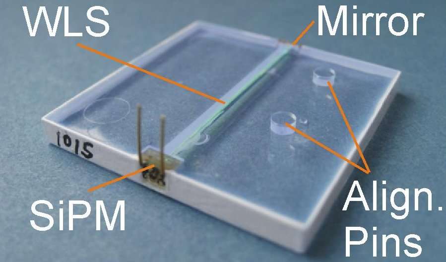
The signal that is detected by the SiPMs is produced by scintillating tiles with a size of cm3, as shown in Fig. 21 left. The new design differs from the design used in the physics prototype [7] and includes a straight wavelength shifting fiber coupled to a SiPM with a size of 1.27 mm2 on one side and to a mirror on the other side. The SiPM comprises 796 pixels with a gain of . Two alignment pins are used to connect the tiles to the HBU’s printed circuit board (PCB) by plugging them into holes in the PCB. The nominal tile distance is 100 m.
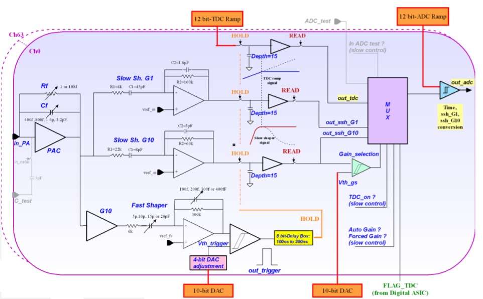
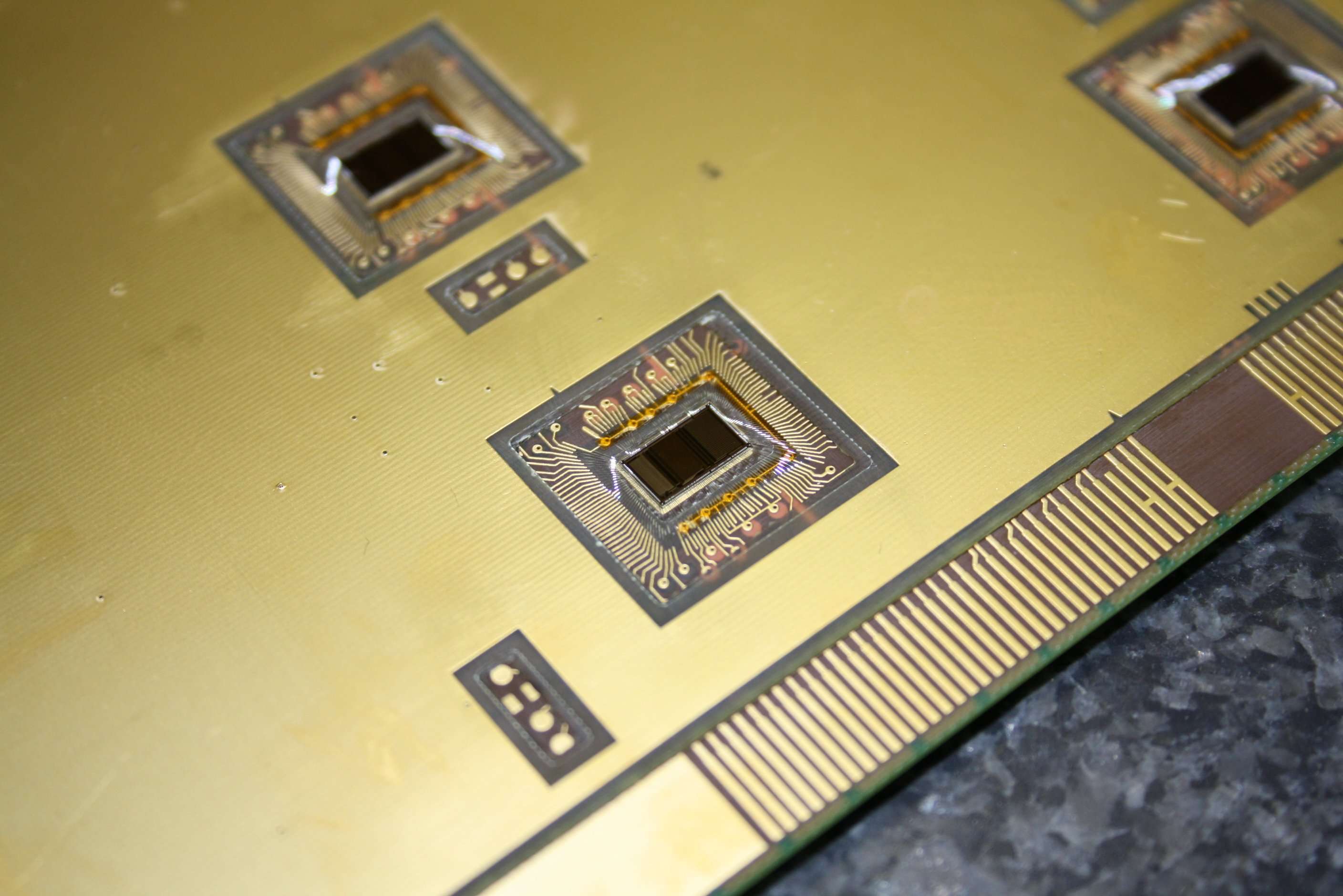
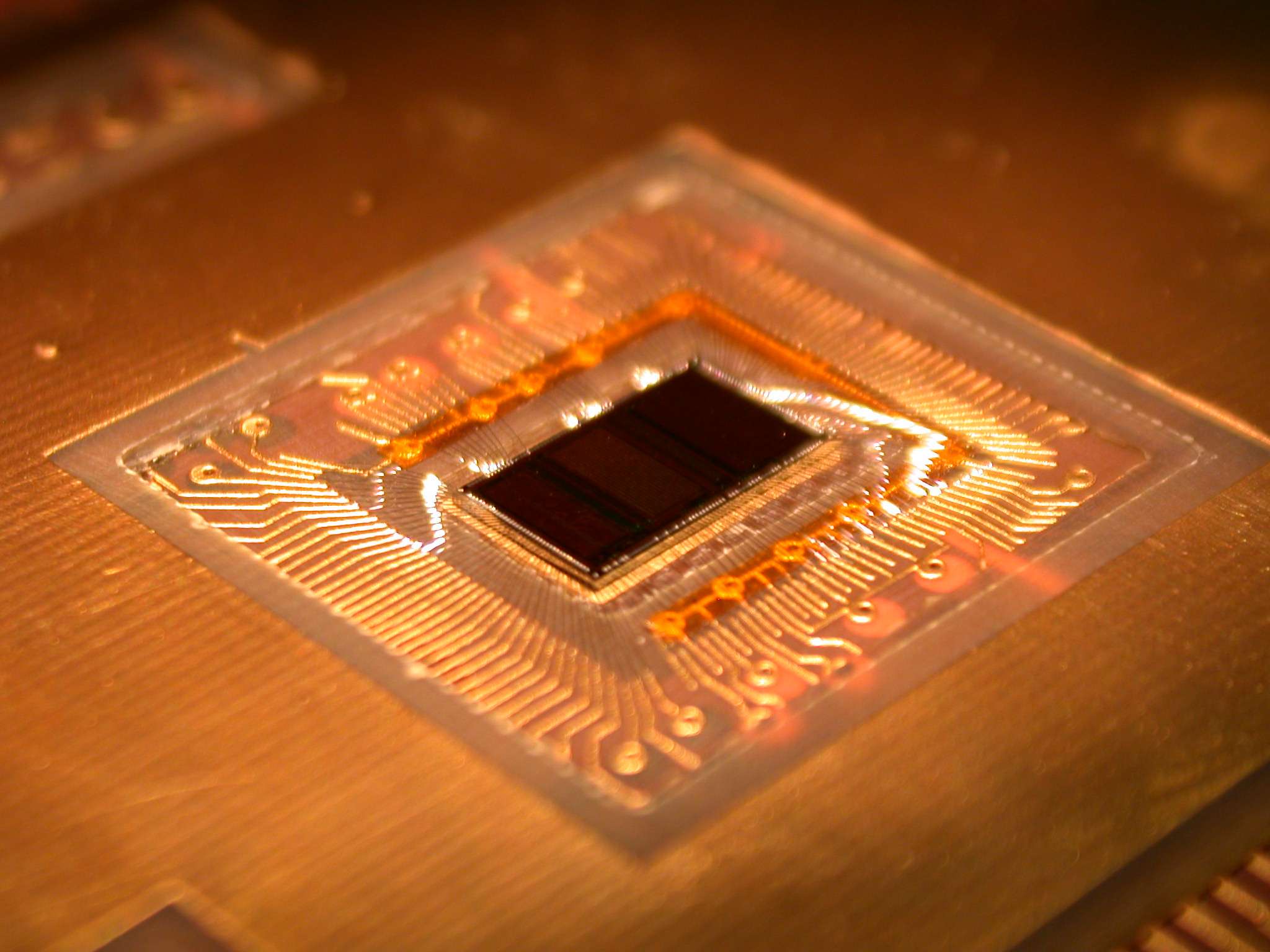
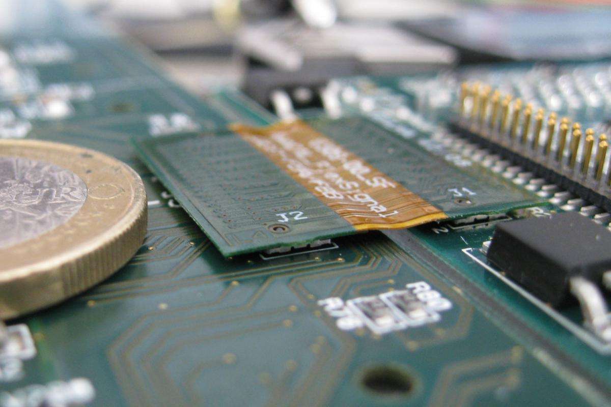
For each HBU the analog signals from the SiPMs are read out by four 36-channel ASICs equipped with 5 V DACs for a channel-wise bias voltage adjustment. They provide two gain modes, which leads to a dynamic range of 1 to 2000 photo electrons. The chips are designed to operate with pulsed power supply for minimized heat dissipation. The foreseen power consumption amounts to 25 W per channel for the final LC operation. The main new features of the ASICs compared to the physics prototype are the integration of the digitization step (12-bit ADC and 12-bit TDC for charge and time measurements) and the self-triggering capability with an adjustable threshold, which acts as a on-detector zero suppression. To reduce the height of the active layers the ASICs are lowered into the PCB by m. This leads to a total reduction of the AHCAL diameter of 48 mm. A picture of an ASIC as it is embedded into the PCB is shown in Fig. 21 right.
5.2 Detector/DAQ interface
Fig. 22 shows the cross section of one AHCAL layer including the dimensions of the single components. The active layers, including the tiles, SiPMs, PCBs and ASICs, are shown as they are placed between two layers of absorber material and connected to the CIB. The total height of the detector/DAQ interface modules hosted by the CIB has to be very small ( 18 mm in case of a tungsten absorber) in order to fit between two layers.
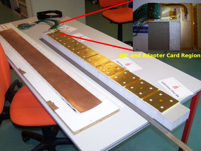
In Fig. 23 the electronics setup is shown in the final assembly stage: The DAQ interface modules DIF, CALIB2 and POWER2 are realized as mezzanine cards on top of the central-interface board (CIB). All modules fulfill the stringent space requirements for an arrangement in the pitch of the absorber plates. All DAQ interface modules have been realized and are in commissioning stage at the moment. The module DIF has been realized by the Northern Illinois University (NIU). It serves as the interface between the inner detector module (HBU) and the back-end DAQ. The CALIB2 module controls the light calibration and gain monitoring system for the SiPMs, which is based on the usage of ultraviolet LEDs. The POWER2 module provides all necessary supply voltages to the inner detector electronics, including the SiPM bias voltages. Additionally, it enables the power-cycling of the HBU electronics in the scheme of the ILC bunch-trains. The final HBU module with the newest generation of readout ASICs SPIROC2b is currently in production.
Up to 10 CIB modules can be connected to one Link and Data Aggregator (LDA) module of the final CALICE DAQ. The LDA collects the parallel incoming data streams of the DIFs on the CIB modules, and serializes the data to a single, duplex optical line, which connects to the backend DAQ (ODR module, not shown in Fig. 23). Timing critical signals as the front-end clock, which is used by all front-end modules for a synchronous operation of all detector parts, are provided from the central experiment through the Clock-and-Control module (C&C). In testbeam setups, the C&C module can be used for the distribution of a fast trigger as well. The setup as shown in Fig. 23 is still in the beginning of the commissioning phase, the prototype has been operated so far by a preliminary Labview DAQ via an USB connection between a PC and the DIF-module.
5.3 Light calibration system
Since the SiPM response shows a strong dependence on the temperature and bias voltage and saturates due to the limited number of pixels, a gain-calibration and saturation-monitoring system with a high dynamic range is needed. In the calibration mode of the ASICs a very low light intensity is needed to measure the gain as the distance between the peaks in a single-pixel spectrum, while at high light intensities (corresponding to 100 minimum-ionizing particles (MIPs)) the SiPM shows saturation behavior. Currently there are two concepts under investigation:
-
•
One LED per tile that is integrated into the detector gap. This system is used in the HBUs in the DESY test setups.
-
•
One strong LED outside the detector, while the light is distributed to each tile via notched fibers (see [8]).
Both options have been successfully tested on the DESY test setups in the laboratory and under testbeam conditions. The measured cross-talk is purely optical and is of the order of 2.5%. The dynamic range of the system redesigned for the construction of the engineering prototype is currently under investigation. The channel uniformity is also an open issue, since for the first LED system the individual LEDs have a large spread of the emitted light intensity, while for the second system the light coupling from the fiber to the tile and its mechanical integration in a full prototype is unsolved.
5.4 Measurements and results
The main task of the current characterization is to prove the suitability of the realized detector-module concept for the larger-scale prototype with 2500 channels and the final length of 2.2 m. Two HBUs are in operation, one in the DESY 6 GeV electron testbeam facility (the 2-6 GeV electrons that have been used are MIPs in the scintillating tiles) and the second in a laboratory environment.
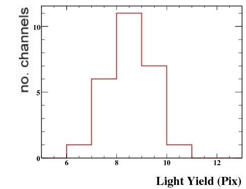
After the investigation of the fundamental properties of the SPIROC chip like noise behavior and signal delays [9], measurements in the laboratory using the LED calibration system and a charge injection setup, as well as testbeam measurements have been performed to investigate the uniformity of the tile/SiPM response for multiple channels. Fig. 24 left shows a typical MIP spectrum measured with the electron testbeam. It can be seen that single pixel peaks are clearly distinguishable for more than 10 peaks. The first peak is the pedestal peak and the maximum of the spectrum is at 9 pixels. The distribution of the light yields, defined as the most probable number of active pixels for a MIP signal, is plotted in Fig. 24 right.
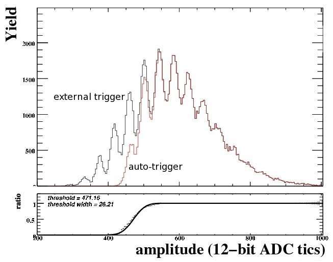
The auto-triggering function of the SPIROC chip has been tested [10]. Fig. 25 left shows two single-pixel spectra measured with LED light and external trigger (black histogram) and auto-trigger (red histogram), respectively. The ratio of the two histograms is also shown and gives an impression of the width of the trigger turn-on curve. After the turn-on the trigger efficiency is 100%.
The threshold of the auto-trigger will be adjusted in order to minimize the noise hits and simultaneously maximize the efficiency for measuring a MIP.
For a threshold requirements of less then than 10-4 noise hits per event, one gets a MIP efficiency of around 95% as illustrated in Fig. 25 right.
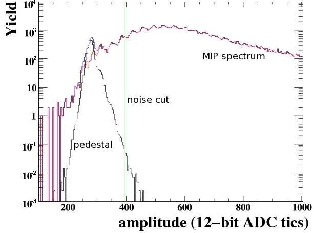
Here the noise threshold is fixed with respect to the pedestal distribution for one given channel (black histogram) and the MIP detection efficiency is calculated from the MIP distribution (red histogram) of the same channels.
5.5 Future plans
In 2011, the system will be further commissioned, including also the timing functionality.In parallel, final versions of the read-out and interface boards are in production, With this, all components are in hand for a multi-module layer tests, using the tile sand new sensors under production at ITEP.
For 2012 a multi-layer test is planned where several options are possible. The HBUs can be arranged in a flexible manner, such that one can instrument an electromagnetic section if the stainless steel module (a tower of 12 HBUs), or produce a few larger area layers (two by tow HBUs) to start exploring time-resolved 4-dimensional shower measurements in the tungsten HCAL. Provided sufficient funding, the second generation prototype will be extended to 40 hadronic layers.
6 Tungsten Analogue HCAL: W-AHCAL
6.1 Motivation
A hadron calorimeter required for the multi-TeV range of the CLIC linear collider will have to cope with increased jet energies. Particle separation will become more difficult and confusion will be of increased importance in the detector resolution when particle flow algorithm is used. But also leakage will be an important contribution to the energy resolution. In the design of the detectors proposed for CLIC a depth of the hadron calorimeter of 7.5 is required. The calorimeter has also to be placed inside the solenoid to achieve optimum resolution. Iron ( cm) as absorber would yield then to a larger radius for the solenoid, which would be costly and difficult to realize. The choice of an heavier absorber material like tungsten ( cm) leads to a substantially smaller solenoid diameter.
However, tungsten needs to be validated as absorber material. A particular question is the influence of delayed neutrons produced by spallation of the tungsten on the shower development. Also the simulation of the hadronic shower development in tungsten has not yet been validated to the same precision as the one in iron as absorber. Therefore a sampling calorimeter has been built using a tungsten absorber and scintillator tiles as readout with a total depth of 4.9 . First experimental data have been taken using a calorimeter depth of 3.9 .
6.2 Experimental prototype
The W-HCAL prototype has been designed in order to use the scintillator cassettes built for the AHCAL physics prototype [7]. The material used in the absorber was a sintered alloy formed by 93% W, 5.3% Ni and 1.7% Cu. This alloy allows easy machining and handling since it is much less brittle then pure tungsten. Each absorber layer has been assembled from 5 square tungsten plates of size and 4 triangular plates with corresponding size to form an octagon with 81 cm diameter (see Fig. 26, left).
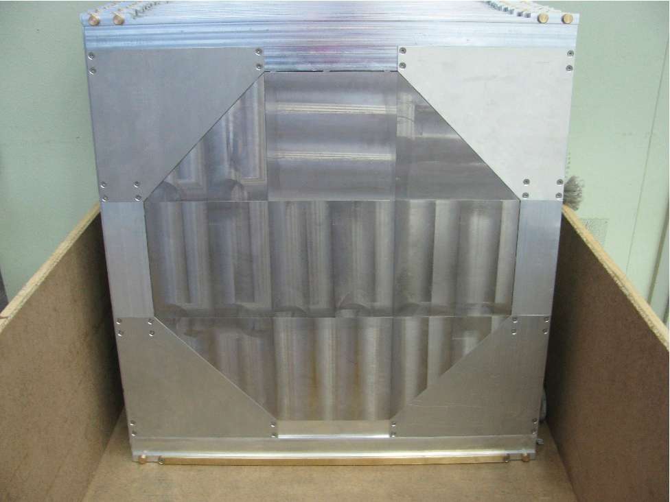
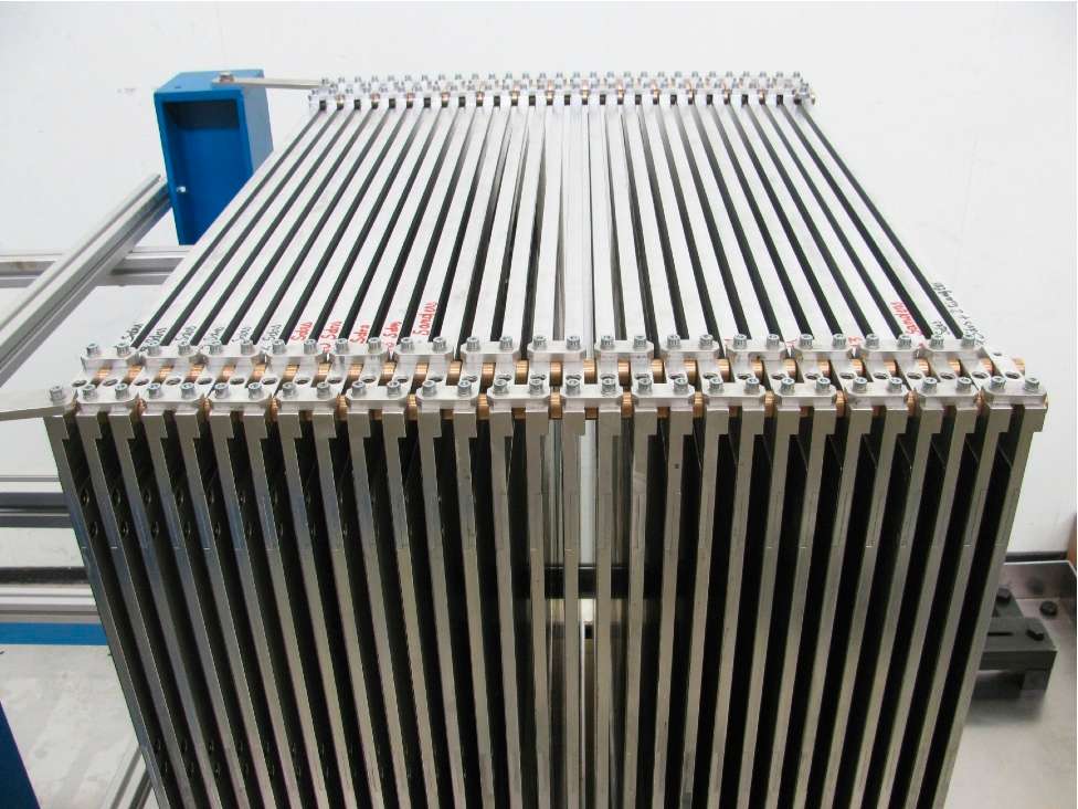
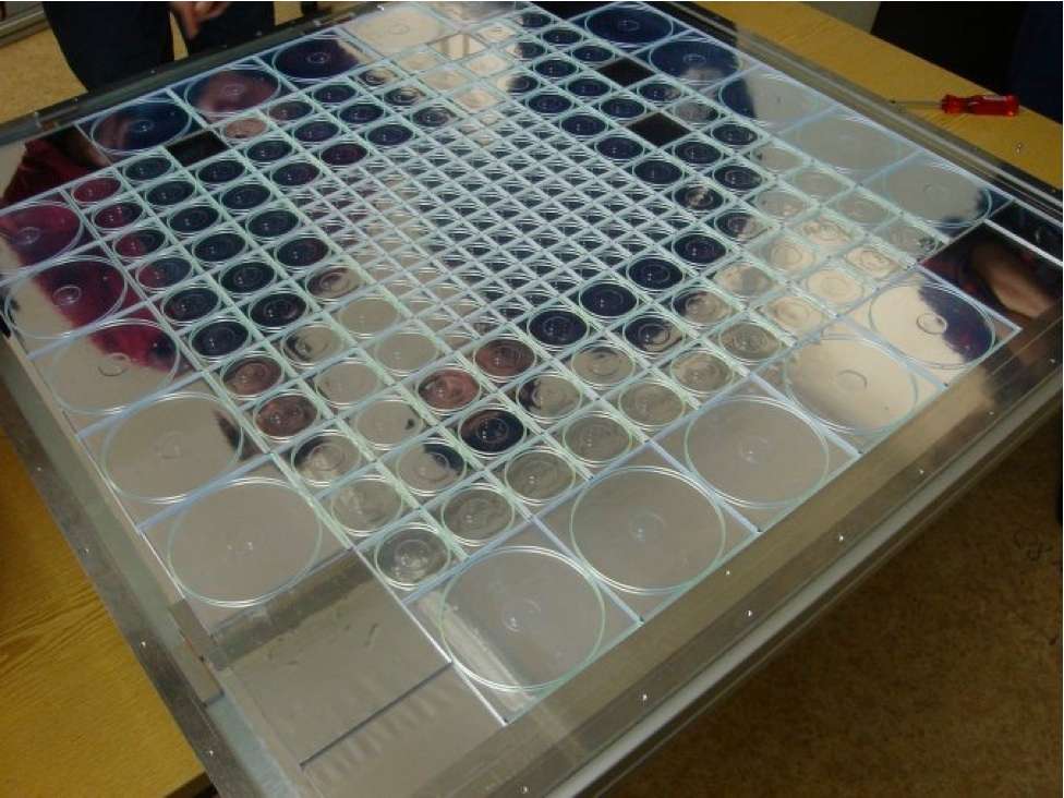
This octagon has been glued into an aluminum frame of a size of m 2. For stability reasons the assembly has been glued to a 0.5 mm thick and 1 m2 sized stainless steel plate. Forty layers with an absorber thickness of 10 mm each have in total been assembled. Thirty and of these layers have been constructed in 2010 and another ten in 2011. The first thirty layers have been assembled in a stack with an interleaving space of 14 mm in between successive absorber layers leaving room for scintillator tile cassettes as active modules (see Fig. 26, right). Each cassette contains 216 scintillator tiles with a thickness of 5 mm: In the central core of the detector are situated 100 tiles with a size of , surrounded by 96 tiles sized . As can be seen in Fig. 27, left, cells with a size of are arranged on the very outside of the cassette.
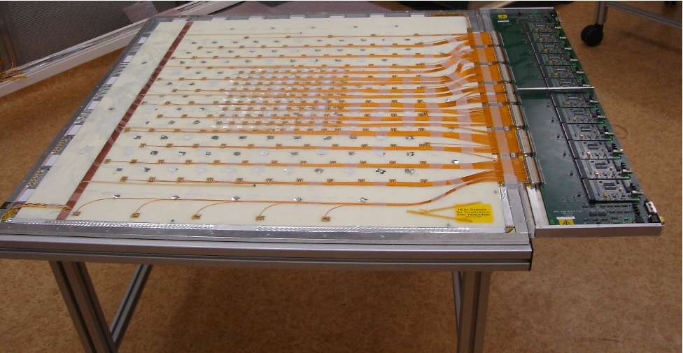
Each tile is read out individually via a wavelength shifting fibre coupled to a silicon photomultiplier (SiPM) mounted on the tile. The SiPM is a multi-pixel avalanche photodiode operated in Geiger mode and provides a gain of more than 105. The scintillator tile layers and the read-out are the same used already in the AHCAL tests with steel absorber in the previous test beams at DESY (2006), CERN (2007) and FNAL (2008, 2009).
The front end electronics is mounted on one side of the cassettes (see Fig. 27, right). It is based on 16 channel ASICs which are read out by the standard CALICE DAQ system. For the calibration and equalization of all the detector channel, test bench characterizations as well as test beam data are used. The detailed procedure is described elsewhere [7].
Minimum ionizing muon beams were used to equalize the cell response. All the cells are equipped with an LED illumination to monitor the gain of each of the SiPMs. In addition the SiPM temperature and SiPM bias voltage have been monitored. Detailed studies of the applied temperature offset corrections were performed.
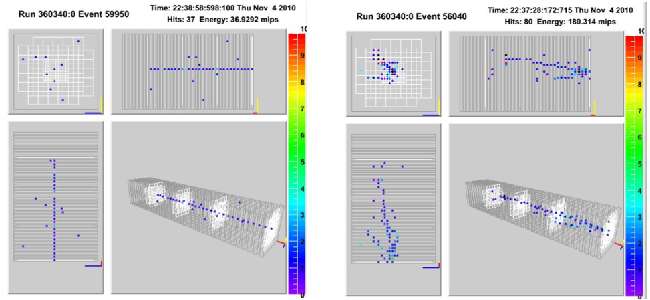
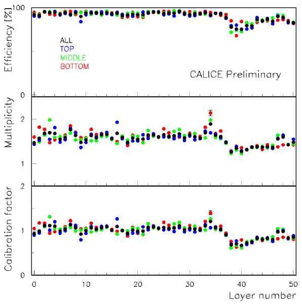
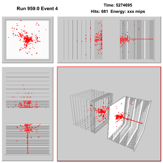
The prototype, equipped with thirty layers of tungsten absorber, has been put into the CERN-PS. About 28 million triggers have been taken using , , and protons in the energy range of 1 to 10 GeV. The beam passed through 2 threshold Cherenkov counters placed upstream in the beam which were used for offline particle identification. Typical events of muon and pions are shown in Fig. 28.
In Fig. 29, left, the energy sum of the total calorimeter is plotted for positrons, muons, pion and protons at 5 GeV. The beam is always contaminated with muons which behave as minimum ionizing particles. Therefore the muon peak is well distinguished for beam energies GeV. In Fig. 29, right, are plotted the calorimeter reponse of muons and pions for energies varying from 1 to 10 GeV.
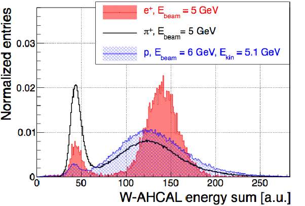
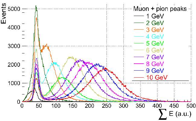
Note that the presented results still use old calibration data (from CERN 2007). However, a first look at the new MIP calibrations indicates very similar calibration values.
We foresee to extend the test in 2011 to an energy range of up to 300 GeV at the CERN-SPS accelerator. From energies of approximately 60 GeV onwards, transversal leakage will become an important contribution to the observed resolution. In order to cope with this, it is planned to add an instrumented tail catcher with a thickness of 6 behind the calorimeter.
6.3 T3B: Time Structure of Hadronic Showers in the W-AHCAL
For calorimeters in CLIC detectors, the time stamping capabilities are of significant importance because of the high bunch crossing frequency of 2 GHz and the high hadronic background from processes. For hadronic showers, the possible time resolution is not only given by the active detector elements, but may well be limited by the intrinsic time structure of the showers themselves. For absorbers with heavy nuclei, such as tungsten, a particularly complex time structure is expected, calling for experimental verification of this aspect of the detector simulations.
To provide first experimental input, a specialized experiment, the Tungsten Timing Test Beam (T3B) detector, was developed and installed in the tungsten analogue HCAL (WHCAL) prototype. A first data taking period at the CERN PS in November 2010 was successfully completed, providing first analysis results [11] that constrain Geant4 physics lists.
6.3.1 T3B: setup and data analysis
The T3B setup consists of fifteen cm2 scintillator tiles with a thickness of 5 mm, directly read out with 1 mm2 Hamamatsu MPPC50P SiPMs with four hundred m2 pixels. The scintillator tiles have a “dimple” drilled into the side face at the SiPM coupling position to achieve a uniform response over the full active area [12]. At nominal operation, they provide a signal of approximately 27 photoelectrons (p.e.) for minimum ionizing particles, including afterpulses of the photon sensor.
The photon sensors are read out with 4-channel USB oscilloscopes222PicoTech PicoScope 6403 (http://www.picotech.com/) with 1.25 GS per second, using long acquisition windows of 2.4 s per event to record the time structure of the energy deposits in the scintillator in detail. Each SiPM was connected to a preamplifier board, which then feeds the signal to the oscilloscope via coaxial cable. The preamplifier boards with packaged scintillator cells were mounted on a 2 mm thick aluminum plate and protected by a 1 mm thick aluminum top cover, forming a robust cassette.
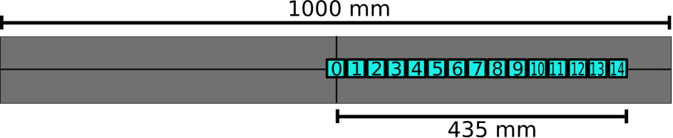
The T3B scintillator tiles are arranged in one row extending from the center of the calorimeter layer out to one side of the detector. The first tile is centered on the nominal beam position, thus the setup extends 15 mm beyond the nominal beam center on one and 435 mm on the other side, as shown in Figure 30. This permits the measurement of a full radial timing profile of the hadronic shower at the position of T3B, given sufficient statistics. The limited coverage however only allows averages over many events to be measured, and is not suitable for the study of the time evolution on an event by event basis.
A first analysis of 645 000 10 GeV events was performed, using T3B in standalone mode without attempting to correlate the events with CALICE WHCAL events to obtain additional information about the showers. The data were analyzed on a cell by cell level. As a first step, zero suppression based on pedestals determined on a spill-by-spill basis was applied. Then, waveforms with an integral above 0.3 MIP were decomposed into individual photon equivalents to provide precise information on the arrival time of photons at the light sensor. This was done by consecutively subtracting single photon signals from local maxima detected in the waveform, until no maxima above approximately 0.5 p.e. remained. The single photon signals were obtained from noise events taken between spills and are determined for each tile separately. This results in an implicit gain calibration, since possible cell-to-cell gain differences lead to corresponding differences in the average single photon signals used in the analysis. The resulting number of photons is thus independent of the SiPM gain. This reference signal was refreshed every 10 spills, typically corresponding to time intervals of less than 5 minutes. This provided continuous automatic corrections of gain variations due to temperature changes.
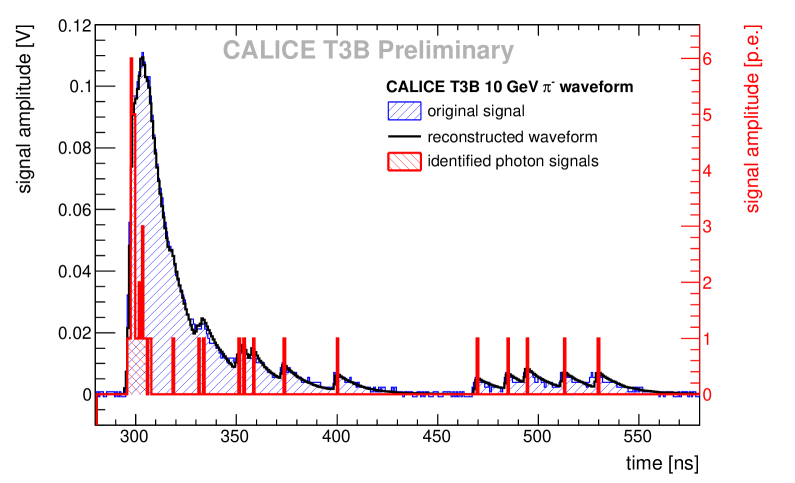
Figure 31 shows one example of a waveform decomposed using this reconstruction technique. To check the quality of this analysis, a waveform based on the identified photon signals was built up with the reference single photon signals and compared to the original waveform. The very good agreement between measurement and the reconstructed waveform demonstrates the quality of reconstruction. First results using this reconstruction are outlined in Sect. 11 below.
7 Digital HCAL: DHCAL
The Digital Hadron Calorimeter Project trades the typical tower structure of past hadron calorimeters and their high-resolution readout with large number of finely segmented active elements, read out individually with a single bit resolution.
7.1 RPC-based DHCAL
7.1.1 Description of the project
A collaboration of institutes (Argonne, Boston, FNAL, IHEP Beijing, Iowa, McGill, Northwestern, and Texas at Arlington) is developing such a novel calorimeter with Resistive Plate Chambers (RPCs) as active media. Currently the readout is segmented into cm2 pads or 10 000 per square metre.
The project progressed in several stages. In a first stage, different designs of RPCs were developed and tested with a high-resolution readout system [13]. In parallel to this activity a 1-bit readout system capable of handling large numbers of channels in a cost-effective way was developed. The second stage put the two together in a small prototype calorimeter, here named the Vertical Slice Test (VST), and included detailed tests with both cosmic rays and in the Fermilab test beam. For the first time within the CALICE collaboration the VST utilized a readout system with the digitization taking place directly on the front-end boards. Based on the successful experience with the VST [14, 15, 16, 17, 18] and after a further round of R&D, the third stage consisted of the construction of a large technical prototype hadron calorimeter (the DHCAL) with, close to 350 000 readout channels. The active elements were inserted into the CALICE hadron calorimeter absorber structure. The calorimeter is now undergoing tests in the Fermilab test beam.
Located behind the hadron calorimeter is the CALICE Tail Catcher and Muon Tracker (TCMT) with 16 active layers. Over the past six month its Scintillator layers have been gradually replaced with RPC layers, identical to the one’s in the DHCAL. This brought the total number of readout channels of the combined DHCAL + TCMT system to approximately 480 000.
Following the tests in the Fermilab test beam, the DHCAL group will return to R&D to tackle the remaining technical issues in preparation of the construction of a so-called Module 0.
Additional information pertaining to this project can be obtained from [19].
7.1.2 Past achievements since the last review
The DHCAL group has been very active since the last review: publishing papers, completing the R&D necessary for the construction of the DHCAL, constructing the DHCAL and the RPC-TCMT, installing the active layers into the CALICE structures in the Fermilab test beam, taking data with various beam configurations, and last but not least analyzing the collected data. In the following we provide a few additional details on these activities:
Completion of the analysis of the VST data.
The 5th and last paper based on data from the VST was published in JINST and documented the environmental dependence of the performance of RPCs.
R&D in preparation of the construction of the DHCAL
Moving from the VST to the DHCAL represented an increase in size and channel count of roughly a factor of 200. Techniques to spray the glass plates with resistive paint providing the required surface resistivity and homogeneity were developed. Fixtures for the preparation of the rims of the RPCs were designed, built and optimized. Three identical fixtures for the assembly of RPCs were built. In order to provide the required uniformity of the gas gap, the fixtures were machined with a precision better than 0.1 mm.
The application of high voltage posed a significant problem, as an attempt was made to minimize the inactive rim around the edge of the chambers. After several set-backs we developed a technique which allowed us to extend the resistive paint up to within a couple of mm from the edge, without the risk of a high voltage break down.
The readout boards consist of a pad board (each with 1536 pads of cm2) and the corresponding Front-end board (with 24 DCAL ASICs), thus avoiding the need for costly blind vias. The two boards are mated to together by applying drops of conductive glue on glue pads on the back side of the pad board. A gluing fixture was designed and built to apply the 1536 glue dots in a timely fashion.
Several prototype iterations were necessary before embarking on the mass production of the front-end boards. The challenge was to minimize the cross-talk between the digital activity of the board and the analog front-ends.
Finally, a viable design of the detector cassette needed to be developed. The role of the cassettes is to: (i) provide a mechanical structure to hold the 3 RPCs in a given layer together, and (ii) to provide a surface to cool the front-end ASICs. Our cassette design exerts slight pressure on the front-end boards against the underlying RPC. This is required to minimize the distance between the two and therefore to reduce the average pad multiplicity for single Minimum Ionizing Particles (MIPs).
Construction of the DHCAL and RPC-TCMT
The construction of the DHCAL and RPC-TCMT took approximately two years and involved up to 15 people at a given time.
Over 700 sheets of glass were sprayed with resistive paint. The procedure was never completely under our control and the efficiency was only about 60%. We made no effort in controlling the environment and abrupt changes in the weather typically required a tedious re-tuning of the various parameters of the spraying gun.
205 RPCs (with the dimensions of cm2) were produced in three parallel assembly lines. The gap size was maintained at a very uniform level, with slightly larger values (100 m) at the four corners. The chambers were tested for gas tightness and the high voltage connections were added. The chambers typically operate at 6.3 kV, but were tested overnight at 7.0 kV.
Over 300 Front-end boards and pad boards were produced. The boards were checked out thoroughly in three test stations, working in parallel. Each test took between 3–6 hours. Faulty boards, with e.g. more than 4 dead channels, were repaired and retested.
Cassettes consisting of a 2 mm copper matched by a 2 mm steel cover, a top and a bottom bar were produced by an outside company. The assembly of the cassettes was relatively straightforward and could be accomplished in less than one hour per cassette.
Of the order of 50 Data collector modules were built and tested at Boston University. Again a dedicated test station was needed to check out the boards. Twelve Timing and Trigger Modules were fabricated and assembled. The check out was done at Fermilab.
New gas mixing and distribution racks were built and commissioned. The RPCs require a mixture of three gases (Freon, Isobutan and SF6). The distribution rack features 28 outputs with individual controls.
The Front-end boards require +5 V. A low voltage power supply system was built which uses commercial Wiener power supplies and custom made distribution boxes. The system provides low voltage to all 306 front-end boards of the combined DHCAL and TCMT system. Each line can be individually controlled and is separately fused.
The high voltage system is on loan from CERN and Fermilab. Due to its relative old age (from the early 1980s), the system is prone to frequent break downs. The group is considering replacing the system with a commercially available system.
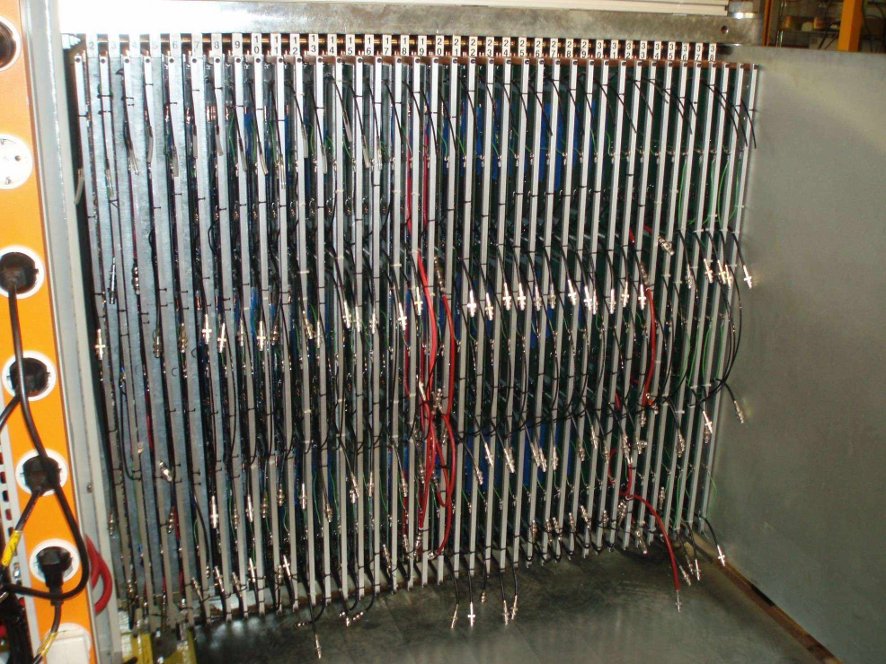
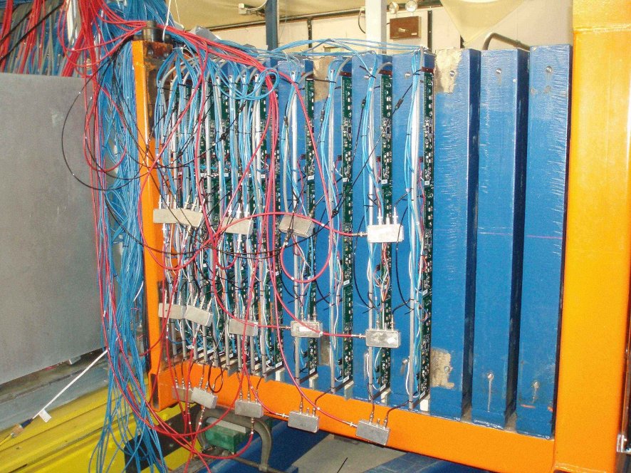
The completed cassettes were transported from Argonne to Fermilab in a specially devised transport structure, which minimized the impact of shocks due to bumps on the road. The cassettes were inserted into the CALICE Hadron Calorimeter absorber structure and into the CALICE TCMT. Fig. 32 shows photographs of the two structures after installation of the RPC layers.
Data taking at Fermilab
Testing of the DHCAL in the Fermilab test beam started in October 2010. Table I summarizes the data taken since. In general the data are of very high quality. The broadband muons were obtained with the 32 GeV/c secondary beam and a 3 meter long iron beam blocker.
As the January run progressed we gradually replaced the Scintillator TCMT layers with RPC layers identical to the ones in the DHCAL. In Tab. 1. the number of RPC – TCMT layers is indicated in parenthesis.
In its current and final configuration the system counts 480 000 readout channels. In April 2011 the CALICE Silicon-Tungsten electromagnetic calorimeter was installed in front of the DHCAL, bringing the total number of readout channels to 490 000.
Due to the rate limitation of RPCs, pion and positron events are collected simultaneously. Separate data sample are generated offline using the Cerenkov signal.
| Date | Configuration | Beam | Number events |
|---|---|---|---|
| Oct’10 | DHCAL+SCINT_TCMT | Broadband muons 1,405 k Secondary beam at 2,4,8,10,12,16,20,25,32 GeV/c 1,524 k | |
| Jan’11 | DHCAL+RPC_TCMT (4-13) | Broadband muons 1,591 k Secondary beam at 2,4,6,8,10,60 GeV/c 3,619 k | |
| Apr’11 | ECAL+DHCAL+RPC_TCMT (14) | Broadband muons Secondary beam | Ongoing |
7.1.3 First DHCAL results
A rigorous effort is underway to analyze the DHCAL data in a timely manner. Due to the fact that the data have been collected quite recently, the results shown here are still preliminary. In order to provide a flavor for the ongoing activities, in the following, we sample results from different analysis efforts. Additional results can be obtained from the DHCAL CALICE notes [20, 21, 22].
-
1.
Analysis of cosmic ray data. The completed chambers were inserted into a cosmic ray test stand and tested with cosmic rays. The stand could accommodate up to nine chambers at a given time. As an example, Fig. 33 shows the distribution of cosmic rays, the efficiency and the pad multiplicity as a function of the dip angle of the cosmic rays.
-
2.
Measurement of the noise rate. The noise rate is measured two ways: i) in trigger-less operation, where any hit in the detector is recorded and ii) in triggered operation during off-beam times, where the trigger is provided by a pulse generator. The two methods are seen to provide consistent results [20]. Fig. 34 shows the noise rate as function of layer number or of RPC number. The average noise rate of 0.6 Hz/cm2 is somewhat elevated for this type of detector and due to the elevated temperature in the stack. Nevertheless, the measured noise rate contributes in average only 0.06 hits or 4 MeV per triggered event.
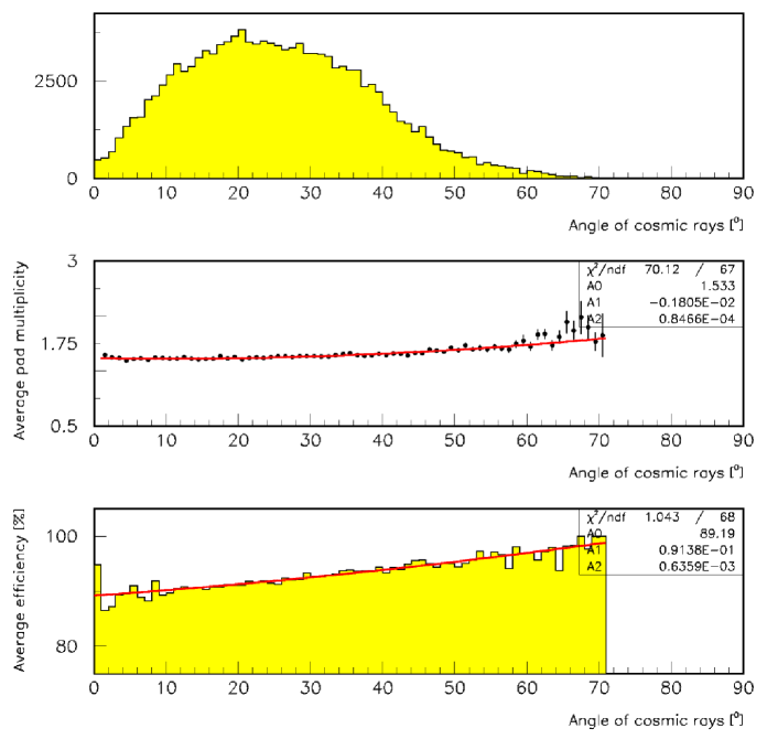
Figure 33: Distribution of cosmic rays, average pad multiplicity and MIP detection efficiency as function of the dip angle of cosmic rays. 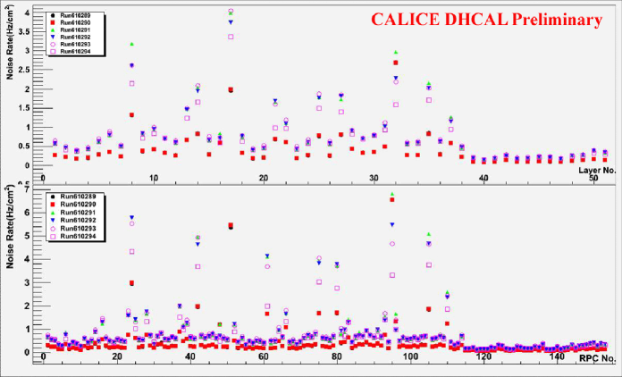
Figure 34: Noise rate in Hz/cm2 as function of layer number and as function of RPC number. The different colors correspond to different runs taken at different times. - 3.
-
4.
Analysis of secondary beam data. Fig. 36 shows the event display of a 60 GeV pion with significant leakage into the RPC-TCMT. Note that the observed isolated hits are not originating from noise, but are generated by the hadronic shower. Some first results based on events like this are outlined in Sect. 11 below.
7.1.4 Future plans
In parallel to the large effort of assembling the technical prototype the collaboration has initiated R&D related to the remaining technical issues of an RPC-based hadron calorimeter. Tab. 2 summarizes the various ongoing and planned activities.
| R&D topic | Funds | Comment |
|---|---|---|
| Thin RPC | Applied for | Further investigation of 1-glass design |
| Large area RPCs | Currently not pursued | Areas of several m2 needed |
| Gas system | Funded | Exploration of new gas mixtures, recycling, gas distribution |
| High Voltage distribution | Funded | System capable of supplying HV to all layers of a module individually |
| Low Voltage distribution | Currently not pursued | System capable of supplying LV to all layers of a module individually |
| Wedge shape | Currently not pursued | Develop concept to accommodate wedge shaped module designs |
| Pad/FE-board | Currently not pursued | Develop new design which minimizes thickness |
| Front-end ASIC | (Funded) | Develop next iteration with reduced power consumption, token ring passing, and redundancy for reliability |
| Data concentrator | Currently not pursued | Develop new system which minimizes space requirement and provides high reliability |
| Mechanical structure | Currently not pursued | Develop cassette structure which can be oriented which ever way, develop module structure which accommodates all supplies and data lines |
| Magnetic field | Currently not pursued | Tests of all subsystems in magnetic field |
7.2 GEM-based DHCAL
7.2.1 GEM 30 cm 30 cm prototype tests with KPiX readout system
A new GEM chamber, with greater ease of assembly and dis-/re-assembly and improved gas flow with new spacers, was designed. In order to use the prototype chamber for beam tests and for integration of KPiX Analog and DCAL digital readout systems, we constructed three of these chambers. After completing one of these new chambers, with the new gas-transparent G10 spacer from CERN and the updated KPiX readout board, we performed source tests using 55Fe and 106Ru radioactive sources. Since 55Fe has characteristic peaks from 5.9 keV and 4 keV X-rays losing their entire energy in the chamber, it provides an excellent test for chamber performance.
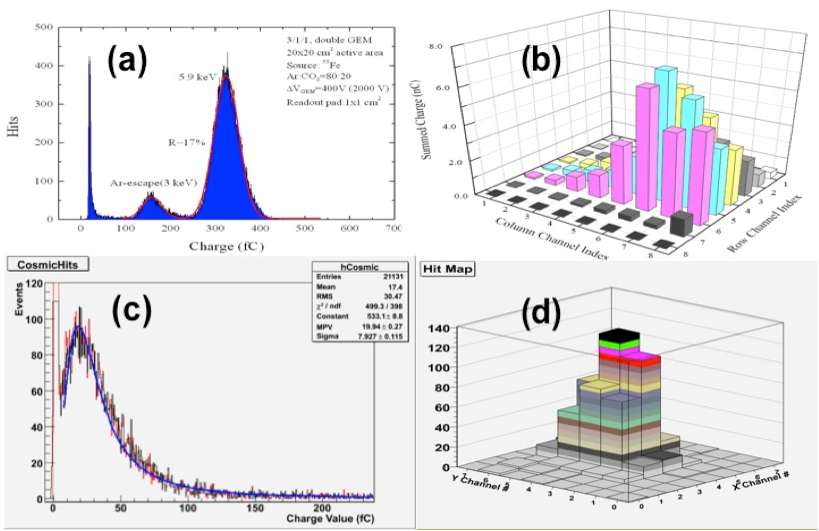
Fig. 37 (a) shows two distinct peaks from 55Fe X-rays in channel 49. The source particles were narrowly collimated to ensure that the particles traversed a normal incidence path rather than with large incident angles. After confirming the minimum ionizing particle pulse height distributions from 106Ru source which shows the typical MIP Landau distributions, we moved into two dimensional measurement by removing the collimator. The source particles are then able to go through various channels demonstrating two dimensional profile distributions in Fig. 37 (b). Fig. 37 (c) shows the characteristic Landau distributions from cosmic ray muons obtained through the 2 cm 2 cm coincidence trigger coverage and plotting the charges from the highest charge pad. Fig. 37 (d) shows the lego plot of the hits from the cosmic ray muons, clearly showing the area covered by the trigger paddles.
We are now in the process of investigating uniformity of the chamber responses by performing response measurements in many different channels. We do see some implication of differences in channel gains a factor of 3.5, we believe this is caused by incorrect application of electronic gains correction in KPiX software. We believe we will resolve this issue shortly working with the SLAC team. Once these issues are resolved, we will be able to determine chamber gains using sources and will take cosmic ray data for further MIP studies and efficiency studies. We will then, as described in detail in the next section, take the chamber to a particle beam for high statistics chamber characterization.
7.2.2 Pressure dependence corrections
Due to the recirculation setup of the Ar-CO2 gas, our GEM chamber gains depend on the atmospheric pressure. We have observed the changes in chamber results over a period in which the atmospheric pressure was known to be changing. Therefore, it is of critical importance for chamber characterization, the chamber gains are corrected for pressure dependence. This section describes the pressure dependence correction.
The measurement was performed using a 30 cm 30 cm GEM prototype chamber read out through the 64 channel KPiX7 chip. The electronics was comprised of two low voltage power supplies, both set at 7 A; one for the FPGA board and another located for the interface board. The GEM detector is directly connected to a high voltage power supply, which is used to set the potentials between the GEM foils. To study pressure dependence, a 55Fe source was elevated a distance above the GEM window and is centered in relation to the readout pads. The pressure dependence of the chamber was studied by performing hour-long runs. The pressure of the local area (City of Arlington, Texas) can be retrieved from national weather services and for each run; and thus subsequent pressure is recorded.
Each hour-long measurement is then analyzed and fitted with a Gaussian distribution where its peak position (peak charge position) is recorded. After multiple data is obtained, a plot of peak position vs. pressure can be made and a linear-regression line made.
The fitted equation from the regression line is obtained where the dependent variable is gain and the independent variable is pressure. It is used to correct for pressure at 1 atmosphere (atm), which is theoretical gain () from the fit. The ratio of theoretical gain, at all the pressures where data was taken, over the measured gain at 1 atm is used as the correction factor (). Using the theoretical gain equation we can input the pressure of the elapsed time for each hour interval and combined with the theoretical gain for that interval and obtain the correction factor, as follows:
| (1) |
7.2.3 Evolution to large area chamber
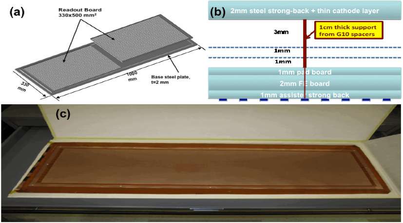
The next step in the evolution of GEM-DHCAL layers is to construct and test a chamber as an element of future planes within a full test beam stack. The team has been working with the CERN GDD workshop in developing GEM foils, the largest foils so far produced to date. The foils have been made using a new single-sided-etching approach, which eliminates some of the manufacturing problems associated with side-to-side registration in the standard double-sided-etching process. The first set of five foils has been produced and delivered to UTA. A procedure for testing and qualification of these foils has been developed based primarily on electrical properties, and all foils have been qualified in three categories. Two of the foils have been identified and ready to be used in the first 33 cm 100 cm.
We have been working on the design of the first chamber and a schematic is shown in Fig. 38 (a) In order to avoid thick side walls for the chamber resulting from tensioning the large foils, we will use a 2 mm steel strong-back on which to mount the chamber. In a final calorimeter configuration, this would be part of the absorber structure between two active layers. The required separation of the cathode, foils and anode layers is achieved by the use of thin spacers, also made for us by the CERN GDD Workshop as shown in Fig. 38 (b). Once we have assembled, tested, and successfully operated a 30 cm 100 cm chamber, we will proceed to construct a full 1 m 1 m plane.
7.2.4 Progress on thick-GEM alternative approach
Since the invention of the standard GEM foil, it has been widely used in various applications and is a promising candidate for use in a DHCAL as discussed above. However, the 50 m thickness can make handling larger foils quite difficult, and there can be issues with dust getting trapped in the 70 m standard hole size. As an effort to overcome such possible drawbacks, another technique has been developed to produce GEMs. In this context we have been collaborating with Weizmann Institute (with travel support from a U.S. Israel Bi-National Science Foundation grant) on thick GEM (THGEM) production and testing using a 0.4 mm thick PCB plate as the base material. Holes with diameter of 0.5 mm are perforated with pitch of 1 mm. For initial tests, two 10 10 cm2 THGEMs were used in the amplification stage and the KPiX readout electronics were used as the data acquisition system. The pressure of the Ne/CH4 = 95/5 gas was kept constant using a containment vessel. The measurement was carried out with gain of 2000, and the measured energy resolution was about 22%. The next step was to try various configurations of single THGEM to achieve a useful level of MIP signal with stable chamber performance. Unfortunately, with the basic THGEM setup read out with KPiX, sparking occurred and two successive chips were found to be dead. We plan to return to the CERN test beam in Summer 2011 and test the “well” and other configurations with later versions of KPiX.
7.2.5 DCAL digital readout integration
In preparation for its digital readout, we have started the effort for integrating the ANL-FNAL developed DCAL readout chip. We spent two weeks at ANL in early 2010 as the initial attempt for integration. While we were able to readout the noise of the chamber and the electronics via the DCAL readout board and back-end DAQ system at ANL, we did not observe a clear signal for detector responses at that time. The timing also did not allow us to continue beyond the allotted two weeks since the ANL RPC-DHCAL team had to prepare for their beam test runs at FNAL. Given this progress and with the help of ARRA funds, we have decided to purchase the back-end DAQ equipment, identical to that of the ANL’s cosmic ray test stand and proceed with two week integration efforts in early 2011. The goals are to fully integrate the DCAL readout board with the prototype 30 cm 30 cm GEM chamber, clearly understand the chamber properties with the digital readout, establish a fully functioning back-end DCAL DAQ system for continued operations and characterization of the chamber with DCAL at UTA. We will construct 2 to 3 chambers fully integrated with DCAL readout system in preparation for the beam tests at FTBF.
7.2.6 Future plans
Through late 2011, the team will complete the characterization of the 30 cm 30 cm chambers, complete the development of 33 cm 100 cm large GEM foils and complete the design of the 33 cm 100 cm foil stretching and gluing stations in preparation for prototype construction. In late 2011 through early 2013 time scale, the team will work on assembly technique for 33 cm 100 cm unit chambers, characterization of 1024 channel KPiXA chips, using 30 cm 30 cm chambers with the intent to use them in 33 cm 100 cm unit chamber, complete understanding chamber behavior with DCAL chips and begin construction of 33 cm 100 cm unit chambers. In early 2013 through mid 2014 time scale, the team will characterize a 33 cm 100 cm unit chamber built with DCAL chip based anode board on the bench and in test beam, construct a 100 cm 100 cm plane using three 33 cm 100 cm unit chambers read out through DCAL chip and build 6 additional 33 cm 100 cm unit chambers for two 100 cm 100 cm planes. Finally in mid 2014 through 2015 time scale, the team will complete constructing three additional 100 cm 100 cm planes and expose to particle beams as a calorimeter in the existing CALICE stack.
8 Semi-digital HCAL: SDHCAL
Members of the CALICE Collaboration, including Belgian, Chinese, French, Russian and Spanish groups, are pursuing a new development aimed at constructing a highly granular gaseous hadronic calorimeter prototype based on a semi-digital readout and a transverse segmentation of 1 cm2. In addition to the tracking capability it offers, a semi-digital readout HCAL can provide very good energy resolution which can be, according to simulations, as good as that of an analogue calorimeter with an appropriate choice of threshold values.
The semi-digital HCAL prototype is intended to come as close as possible to the hadronic calorimeters of the future ILC experiments in terms of resolution, efficiency and compactness. For instance, they should have negligible dead zone in order to keep the tracking capability as high as possible. They should also be very thin to reduce the cost of the whole experiment. Indeed, as the HCAL will be placed inside the magnetic field, reducing the thickness of the sensitive media is essential to avoid an excessively large radius of the magnet coil, which would have very serious cost implications for the overall detector.
Two kinds of gaseous detectors are being investigated as candidates to become the sensitive medium of such a SDHCAL: glass RPCs (GRPC) and MICROMEGAS. New readout electronics satisfying the ILC constraints was developed and successfully tested on small GRPC detectors and more recently on a 1 m2 detector.
8.1 RPC-based SDHCAL
The use of gaseous detectors such as the GRPC ensures excellent efficiency and good homogeneity of the sensitive medium at a low cost. In contrast to the other options, the high granularity of this gaseous HCAL option is provided by the readout electronics system. The signal created by the passage of charged particles in GRPC detector is collected thanks to 1 cm2 pads etched on one of the two faces of the electronics board and put in contact with the GRPC. To keep the the sensitive medium as compact as possible, the readout ASICs need to be tiny, embedded on the detector and connected with each using the electronics board itself thanks to a DAISY chain scheme. This leads to a limited number of connections coming out of the sensitive medium. With such a granularity more than 50 million electronics channels are needed for the HCAL of the ILD experiment. This renders the analog readout prohibitive from the acquisition point of view.
Aa a trade-off, a 2-bit readout is proposed. The choice of this semi-digital scheme rather than the binary one was motivated by simulation studies which show that better performance can be obtained by the semi-digital scheme at high energy. This result can be explained by the fact that at high energy many particles might go through one pad especially in the centre of the hadronic shower. Since the extension of the avalanche created by charged particle in GRPC is of the order of few square mm [24], the semi-digital readout with its three thresholds can help to distinguish among scenarios with few, many and too many particles going through one pad. This improves the energy resolution by providing a better estimate of the number of charged particles produced in the hadronic shower, and also in separating the electromagnetic and the hadronic contributions.
The technology mentioned above was successfully tested with small GRPCs [25]. Large GRPCs of 1 m2 size were then developed using new concepts with the goal to keep the detector as homogenous as possible. Electronics boards were also designed to cope with the large detector surface and a compact cassette was conceived to tie them together. The successful tests of two of those cassettes in cosmic ray test benches, as well as in test beam at CERN, paved the way to start the construction of a technological prototype of 1 m3. It is intended that this will be completed in May 2011.
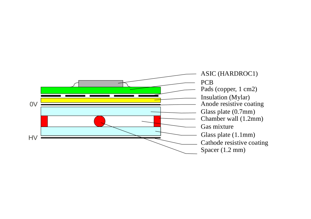
8.1.1 Detector design
As can be shown in Fig. 40 the GRPC is made of two glass plates of 0.7 mm and 1.1 mm thickness. The thinner is used to form the anode while the the thicker forms the cathode. 68 Ceramic balls of diameter 1.2 mm are used as spacers to separate the glass plates. The balls are glued on only one of the glass plates. In addition to those balls, 13 cylindrical buttons of 4mm diameter made of fiber glass are also used. Contrary to the Ceramic balls the buttons are glued to both plates ensuring thus a robust structure.
The distance of the spacers (10 cm) and hence their number was fixed so that the deviation of the gap distance between the two plates under the glass weight and the electric force when the high voltage is applied on the two electrodes does not exceed 45. The choice of these spacers rather than the fishing lines was intended to reduce the dead zones (0.1% ) rather than the few percents in the case of the fishing lines. It was also aimed at reducing the noise contribution observed along the fishing lines in the small GRPC chambers.
The gas volume is closed by a glass fiber frame of 1.2 mm thick and 3 mm wide glued on both glass plates. The glue used for both the frame and the spacers was chosen for its chemical passivity and long term performance. The resistive coating on the glass plates which is used to apply the high voltage and thus to create the electric field in the gas volume was found to play important role in the pad multiplicity associated to a MIP. To find the best coating for our chambers many products were tested. Finally two products were identified, both of which are based on colloids containing graphite and both can be applied using the silk screen print method which ensures very uniform surface quality. Both were found to provide stable resistivity in the range 0.5-2 M/Square. Repeatability tests were conducted to validate the use of such coating for a large amount of detectors. Both products can be painted using the silk screen printing method which guarantees very good homogeneity. Another important aspect of this development concerns the gas distribution within the GRPC. In order to improve on the gas distribution in large chambers taking into account the requirement that both gas outlets should be on the same side of the detector to satisfy all possible mechanical structures proposed for ILD hadronic calorimeter, new schemes were studied. The one we finally adopted is based on channeling the gas along one side of the chamber and releasing it into the main gas volume at regular intervals thanks to a PEEK tubes of 1.2 mm diameter fixed at 5 cm from the chamber side. A similar system is used to collect the gas at the other side of the chamber. A finite element model has been established to verify the gas distribution [26]. The simulation confirms that the gas speed is reasonably uniform over most of the chamber area.
8.1.2 Electronic readout
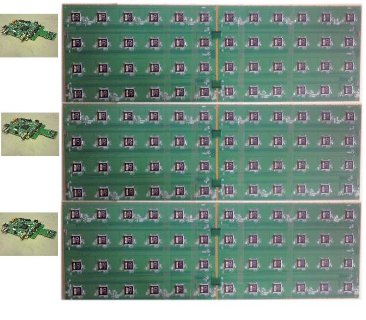
To read out the 1 m2 GRPC detector, an electronic board with the same size is needed. This electronic board is an important piece in the present design. It hosts both the pick-up pads and the ASICs in addition to the connections linking the pads to the ASICs as well as those among the different ASICs. To ensure good transmission qualities and low cross-talk, 8-layer ASU (Active Sensor Unit) was conceived. Feasibility constraints, make the tasks of circuit production, components soldering, testing and handling of the assemblies, exceedingly difficult in the case of a single board of one square meter. The solution of dividing that circuit into 6 smaller but more manageable ASU boards was adopted.
Each of these small ASUs hosts 24 Hardroc chips to read out pads of 1 cm2 each. The routing of each input signal from its own pad up to the HARDROC pin has been carefully optimized to reduce the cross-talk. All input signals are laid out in the same analog signal layer which is sandwiched between two GND layers. Great care has been taken keeping the routing of digital signals well separated from the vias connecting signals from one layer to another.
The HARDROC base pattern is then replicated 24 times in the cm2 small board following a form factor. The rooting was conceived so two of the ASUs can be associated to form one slab hosting 48 ASICS. Each slab is then connected to one DIF (Detector InterFace board). The connection between the DIF and the slab as well as the connection of the two ASUs is performed thanks to tiny connectors allowing the different clocks, signals as well as the power to circulate between the two ASUs. Three slabs are then assembled to form the required electronics board. To ensure the same electric reference level for the six ASUs, the GND layer of the six ASUs is connected thanks to a copper gasket on all the common sides. The thickness of the final electronic board taking into account that of the HARDROC chip with its TQFP160 package is less than 3 mm. In Fig. 40 a picture of the electronic board of 1 m2.
8.1.3 Data acquisition
To communicate with the different ASICs of one slab a board called Detector InterFace (DIF) was conceived. The DIF hosts an FPGA device which by distributing the DAQ commands to the ASICs and by transmitting the collected data to the DAQ system constitutes the master piece of the DIF.
In addition to the FPGA the DIF hosts the connectors allowing the communication with the slab on the one hand and with the DAQ system on the other hand. Two kinds of connections with the DAQ system are available: A USB-based and and HDMI-based ones. Furthermore, The DIF is used to power the slab. The first phase of the acquisition is the transmission of the configuration parameters to the 48 ASICs of one slab. Indeed configuration parameters are transmitted through the FPGA. Once the ASICs are configured, the second phase can start. In this phase the communication between the DAQ and the ASICs can be summarized in two steps: an acquisition phase and a readout one. The second phase starts after the end of the first one due to an external signal which can be triggered by a full-memory state (RAMFULL). The readout of each ASIC is performed after receiving a StartReadout and ends by emitting an EndReadout commands. The latter is transmitted to the next ASIC which interprets it as a StartReadout command. The readout phase of each ASIC can last up to 4 ms in the worst case when the 127-frame memory is full. As was mentioned before, to read out large GRPC detectors with a 1 cm2 lateral segmentation many ASICs need to be assembled. To keep small the number of connections between the ASICs and the DAQ system the ASIC digital readout signals were conceived to be linked to an open collector bus and hence daisy chained leading to only one connection. This is also the case for what concerns the assignment of configuration parameters to all the ASICs of one board. The situation is different with respect to the acquisition where all the ASICs should start this phase at the same moment. To synchronize the previous operation among the ASICs of one slab as well as that of the three slabs, the DIF can be connected with each other and the commands to stop and start the acquisition is transmitted simultaneously to the 144 ASICs. This is also true in the case of a RAMFULL. This scheme was used for validation tests. It will be soon replaced with the CALICE second generation acquisition system is under development and will be used in the hadronic calorimeter prototype with its 144 DIFs. The acquisition system will be based on the Xdaq software developed for the CMS tracker acquisition. More information on this can be found in the CALICE acquisition section.
8.1.4 Cassette
As mentioned before, the GRPC and its associated electronics are housed in a special cassette which protects the chamber and ensures that the readout board is in intimate contact with the anode glass. The cassette is a thin box consisting of 2.5 mm thick stainless steel plates separated by 6 mm wide stainless steel spacers which form the walls of the box. These spacers are precision machined so no space left between the two cassette plates and the sensitive medium. The dimensions of the plates are such that a space of 2 mm wide is left between the GRPC and the cassette’s walls. This space is filled with insulating product to protect against sparks. One of the two plates is 20 cm larger than the other. This allows one to fix the three DIFs as well as the gas outlets and the high voltage connector.
The electronics board is assembled thanks to a polycarbonate spacer which is also used to fill the gaps between the readout chips and to improve the overall rigidity of the detector. The board is then fixed on the small plate thanks to tiny screws and the new set is fixed on the other plate which hosts the detector and the spacers. The whole width of the cassette is 11 mm with only 6 of them corresponding to the sensitive medium including the GRPC detector and the readout electronics.
8.1.5 Tests and results
The cassette including the GRPC and the associated electronics described in the previous section was first tested in a cosmic rays bench. The bench was equipped with a triggering system made of two scintillator-PMs. One is placed above the cassette and the other beneath. In order to evaluate the homogeneity of our detector response we equipped the bench with a movable structure with two arms on which we fixed the scintillators. The scintillators position can be chosen easily. We have however selected three positions corresponding to a geometrical areas read out by three different slabs (and hence three different DIFs). To ensure the absence of fake triggers due to the scintillator noise and to have a rather precise information on the particle impact in the GRPC, the same setup that was used to study the small GRPCs as described in reference [25] was used. This setup made of 5 small GRPCs ( cm2) equipped with the same readout electronics was fixed on the aforementioned structure that supports the scintillators and used as a tracker. Both the large GRPC as well those of the tracker system were operated with the following gas mixture: Tetrafluoroethane (TFE, 93%), Isobutane (5%) and SF6 (2%). Since the large GRPC and the small ones are not equipped with the same acquisition a DIM-based protocol was used. The protocol allows to accept triggers only if none of the GRPCs readout electronics is busy. This ensures that the two systems are stooped simultaneously with the occurrence of an external trigger and their memories are read before to start again recording data as described previously. This procedure allows to associate the hits due to the same trigger in both the large and small chambers.
The polarization voltage of the small GRPC chambers was fixed at 7.4 kV. This was found to provide the best efficiency as described in [25]. The efficiency and the pad multiplicity of the large chamber was then studied by varying its polarization voltage in the range 6.2–8 kV. The hits belonging to the small chambers were then used to build tracks following the same method described in [25]. The coordinates of the particle impact on the large chamber are then deduced. An uncertainty of less than 1 mm in both direction is expected from the straight line fit applied on the small chambers hits. The hits of the large chamber belonging to the same time window are then looked for and their coordinates are compared with the that of the particle impact. If at least one hit is found in the vicinity of the impact particle (a zone of 2 cm radius around the particle impact) then the hit is considered to belong to the track. The number of hits found with a distance less than 5 cm with respect to the impact coordinates provides the pad multiplicity associated to this track. The efficiency obtained for the three different zones was found to be almost identical and the pad multiplicity in the range of 1.6 to 2.3 pads/MIP. The homogeneity observed in the results obtained in the three zones indicates that both the detector and the readout electronics are homogeneous. The noise was also measured and found to be about 1 Hz/cm2. The cassette was then exposed to a pion beam of 10 GeV at the the T9 beam line of the CERN-PS.
A triggering system using four scintillators-PM was used with two of them were placed upstream and the two others downstream. The scintillators position was chosen so a particle passing through the four of them passes necessarily in the GRPC chamber. The cassette was placed on a movable stage with X and Y movement. Due to a space limitation only two thirds of the cassette could be exposed to the beam. Contrary to the cosmic-rays -bench test the small GRPC setups was not used here. In addition and because of CERN safety norms the isobutane was replaced in the gas mixture by CO2 with the percentage.
To check the GRPC behavior in a beam and in the vertical position in opposition to the horizontal one of the cosmic-rays-bench test, the central zone behavior was studied by varying the polarization voltage. Although the gas mixture is not identical we observe the same efficiency behavior as the one obtained with the cosmic rays test was observed. The same statement is valid for the pad multiplicity.
The second step was to confirm the homogeneity of the detector. 13 zones corresponding to different positions of the electronics board and the detector were chosen as shown in Fig. 41. For all these positions the GRPC was operated at the same polarization voltage of 7.4 kV. The results obtained for all those positions are shown in Fig. 41. They confirm those found in cosmic-rays-bench test. These results with the vertical position show that the cassette we conceived provides enough rigidity to maintain the electronics board in contact with the GRPC detector.
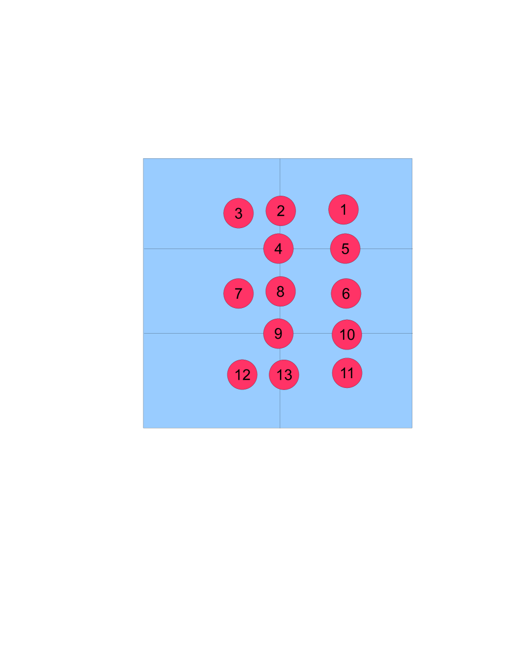
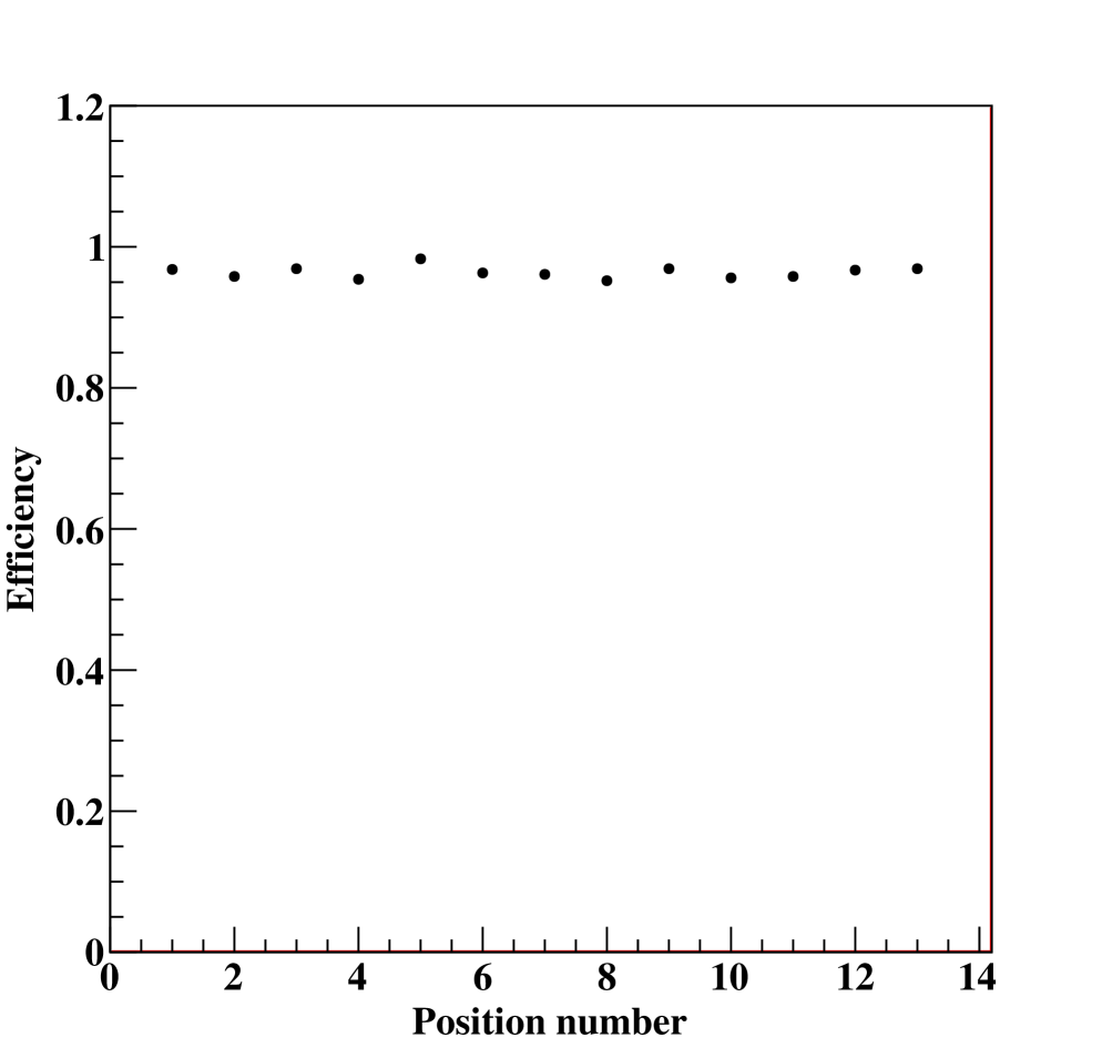
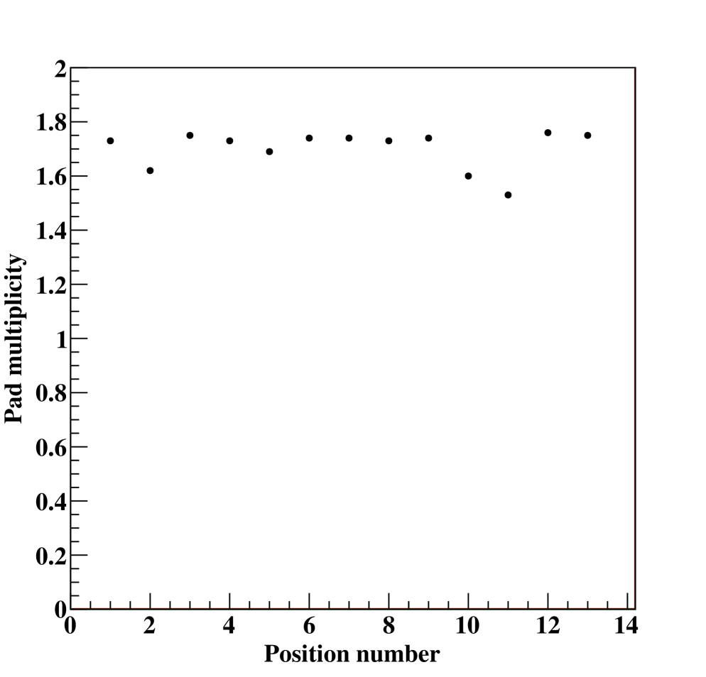
An important test to validate the power-pulsing scheme in a magnetic field of 3 T was performed in the H2 magnet of the SPS-CERN in 2010. The results obtained with a fully equipped detector of cm2 showed that the power -pulsing scheme which allows to reduce the power consumption considerably when applied to the ILC duty cycle of 1 ms of cross-benching every 200 ms is functional and no loss of efficiency was observed.
8.1.6 Mechanical structure
A self-supporting structure was conceived to host the 48 cassettes needed for the technological prototype. It is made of 48 stainless steel plates of 1.5 cm thickness each. The plates should satisfy stringent conditions on flatness and thickness resolutions (250 m and 100 m respectively). They are assembled together thanks to spacers of ( mm2) section precisely machined. Three spaces are indeed used to assemble two consecutive plates thanks to well distributed bolts. This leaves a 13 mm to insert the previous cassette. The deformation of such structure was carefully study in different positions and found negligible on the HCAL performance. The mechanical structure is being indeed built and the first tests show that the results are in agreement with expectations. The whole structure will be completed in May 2011. In addition to this structure a rotation tool allowing to use the prototype in vertical and horizontal position has already been built.
8.1.7 Prototype construction
The technological prototype construction has started in late 2010. More than 30 GRPC satisfying the requested quality control were already built. The cassettes described previously were all produced. The electronics board are being produced and cabled with the HARDROC ASICs which have been all tested thanks to a dedicated robot. The electronics boards production as well as the assembling process are expected to be completed in May 2011.
After a period of 1 month commissioning the prototype will be exposed to particle beams at CERN first in late June and then in October. The first period will be used essentially for calibration study and optimization procedure while the second will be dedicated to physics study.
8.2 MICROMEGAS-based SDHCAL
Invented in 1996, MICROMEGAS is today widely used in several running experiments (COMPASS, KABES, T2K) and is also considered for LHC upgrades (SUPER-ATLAS) and at future electron colliders (ILD TPC). The rapid progress recently made on Micro Pattern Gas Detectors (MPGD) makes MICROMEGAS a viable choice for a semi-digital hadronic calorimeter. With the Bulk technique developed by the CERN technical service MICROMEGAS becomes a robust detector which satisfies the requirements of thickness, efficiency and large area. In addition, it has working voltages below 500 V and is insensitive to neutrons if used in hydrogen free gas mixtures. Finally, it delivers signals proportional to the deposited energy and demonstrates very high rate capability (up to some GHz/mm2): MICROMEGAS is thus well suited for a multi-threshold readout and could instrument both the barrel and forward regions of a linear collider experiment (ILC or CLIC).
8.2.1 Small prototypes
Baseline parameters of MICROMEGAS chambers are 3 mm of argon-based gas mixture (with iC4H10 or CO2) and square pads of 1 cm2 (Fig. 42). First prototypes were small chambers with dimensions up to 3212 cm2 equipped with analogue readout electronics based on GASSIPLEX ASICs. At a detector gas gain of 104, the measured most probable value of the charge from MIPs is 25 fC with 10 % variation over each chamber pads. Most importantly, the efficiency to MIPs reaches 97 % (at 1.5 fC readout threshold) with 1 % absolute variation per chamber. Due to very little transverse diffusion in the gas volume, the fired pad multiplicity lies below 1.15 even at the lowest workable thresholds [27].
Small prototypes have been first used for characterisation (2008–2009) [28, 29, 30] and more recently (2010) as a telescope during the test in a beam of the first MICROMEGAS chamber of 1 m2. Over the three years, they showed constant performance and resistance to gas discharges thanks to dedicated protections between the pads and the ASIC inputs.
8.2.2 Active sensor units of 4832 cm2
The basic units composing the 1 m2 MICROMEGAS chamber are 1 mm thick Printed Circuit Boards (PCB) of 4832 cm2 with anode pads and Bulk mesh on the top side and embedded readout ASICs and discharge protections (passive components) on the opposite side (Fig. 43). They are called Active Sensor Units (ASU). The fabrication proceeds first with soldering the ASICs and protections to the PCB. In order to laminate the Bulk mesh on the pad side, a mask is then glued on the ASIC side; the final ASU thickness is 3 mm. This together with the 3 mm drift gas gap yield a minimal thickness of a Micromegas chamber of 6 mm (baseplate and cover, being part of the absorber, are ignored).
A detailed calibration procedure of the ASICs has been established to measure the pedestals and noise levels of each channel (1536/ASU). Eventually this information is used to correct for the channel to channel non-uniformity by tuning the preamplifier gains or to lower the individual detection thresholds by aligning the pedestals to a central value.
8.2.3 First prototype of 1 m2
The design of the m2 chamber consists of 6 ASUs placed next to each other inside a common gas volume (Fig. 44 left). Spacers are inserted in the 1 mm gap between boards to define the 3 mm drift gap. Together with 2 mm wide insulating lines on the ASU edges to support the Bulk meshes, they are responsible for dead regions of about 2 % of the total area inside the chamber. The first m2 prototype was assembled in May 2010 from 5 ASU each equipped with 24 HARDROC2 ASICs. Although the fast HARDROC2 shaper is not suitable for the 150–200 ns long MICROMEGAS signals, no other chip was available in required quantity at that time. It was hence decided to build and test the prototype in order to validate the design as well as several technical choices (materials, assembly procedure, gas distribution, feedthrough…).
8.2.4 Beam test
The m2 prototype was tested in a high energy muon beam in June/July 2010 at the CERN SPS (Fig. 44). At the nominal gas gain of 104 a pad efficiency of 50 % was reached. This value was expected from the fast shaping of the HARDROC2 chip which makes use of roughly 10 % of the detector signal only. A pad to pad study performed with a telescope revealed no significant spatial dependence of the detector response. The prototype was also tested under power-pulsing of the ASIC analogue parts (2/10 ms ON/OFF). Efficiency measurements with and without pulsing yielded similar results.
At the end of 2010, the MICROMEGAS group joined the test of the tungsten analogue hadron calorimeter (W-AHCAL) in a beam of low energy hadrons at the CERN/PS (Fig. 45). The m2 prototype acted as the last layer and recorded hits from hadrons showering deep in the calorimeter. A synchronisation between the two acquisitions could be set up which should allow the reconstruction of events recorded by both detectors. The analysis of the data is on-going though preliminary results of standalone reconstruction have been obtained.
8.2.5 ASIC development
In collaboration with the LAL/Omega group and based on the experience obtained with the HARDROC2 and DIRAC circuitry [31], LAPP is developing a new ASIC. Optimised for the detection of MICROMEGAS signals (and also GEM/THGEM signals), this new chip is called MICROROC and has 64 channels with individual pedestal settings and three thresholds common to all channels. Oriented for use at a future linear collider, it has a 127 event depth memory and power pulsing capability.
A batch of 350 chips has been fabricated in 2010 and caracterised on a test board. First measurement of the noise level (around 0.24 fC) allows the detection of input charges down to 1 fC. Systematic calibrations are now on-going on the full batch and already half of the chips have been tested and mounted on 7 ASU. These will compose a new 1 m2 prototype which should be ready for test in July 2011. The construction of a second prototype with MICROROC should be completed by fall.
8.2.6 Future plans
The short term plan is to test at CERN the first MICROROC prototype of 1 m2. A test in a muon beam should be carried out in August 2011, followed in fall by a test inside steel or tungsten structures of one or two planes. In the latter case, the MICROMEGAS group intends to join the test of the Glass RPC Fe-DHCAL and/or the scintillator W-AHCAL.
Longer term plans are the fabrication of more MICROROC ASICs and prototypes. The number of planes to be produced in 2012 and later critically depends on financial ressources and is thus not precisely known today. Shower development and containment of low energy electrons and hadrons can already be studied with a small number of planes. Future test in beams should therefore be conducted inside steel or tungsten structures, preferably at the CERN PS facility.
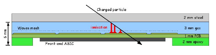
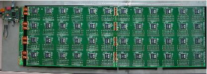
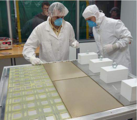
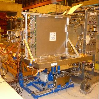
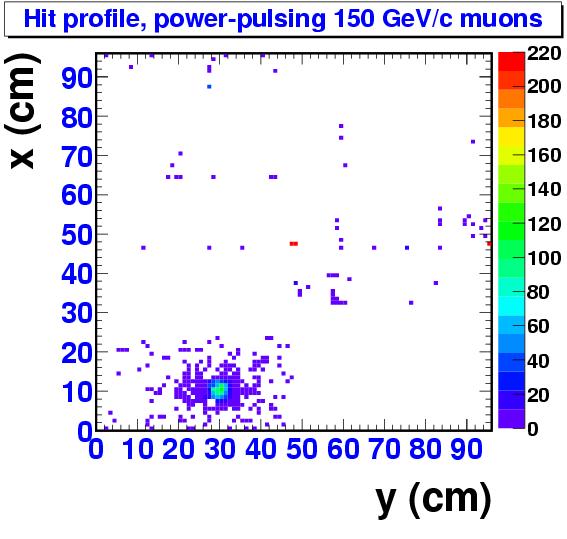
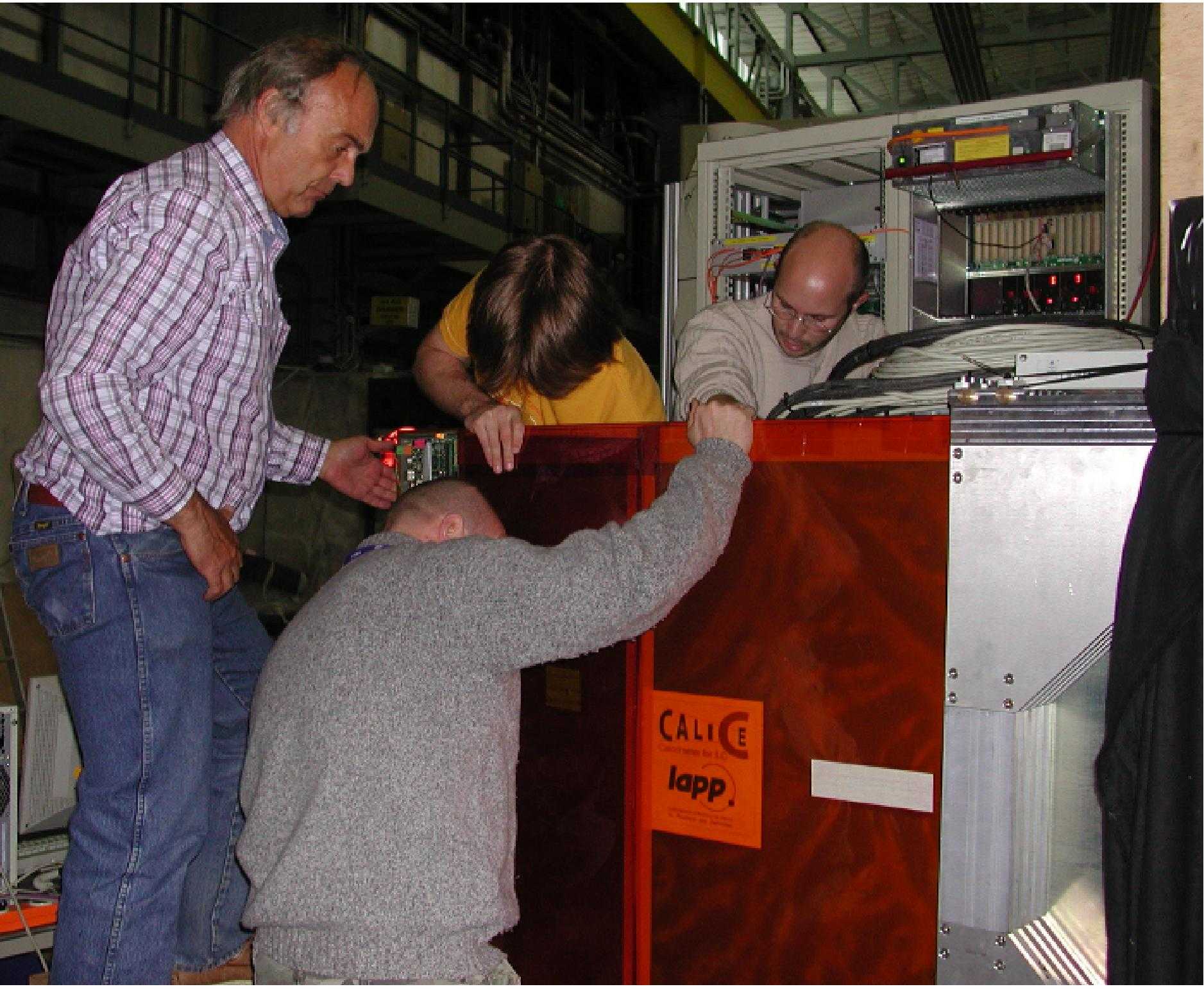
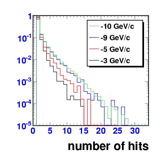
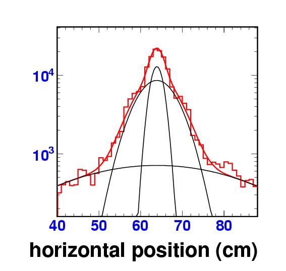
9 Front-End Electronics
A second generation of readout ASICs have been developed to read out the technological prototypes defined in EUDET and CALICE. These are based on the first generation of chips that were used for the physics prototype for the analogue front-end part but add several essential features:
-
Auto trigger to reduce the data volume
-
Internal digitization to allow purely digital data output
-
Integrated readout sequence and common interface to the second generation data acquisition to minimize the number of lines between chips
-
Power-pulsing to reduce the power dissipation by a factor of 100
Three chips have been designed, following the EUDET milestones:
-
HARDROC for the digital Hadronic Calorimeter, for RPCs or Micromegas chambers. A new ASIC, MICROROC, has also been designed and submitted in June 2010 for 1m2 MICROMEGAS detectors, which require HV spark robustness for the electronics and very low noise performance to detect signals down to 2 fC.
-
SPIROC for analog Hadronic Calorimeter.
-
SKIROC for the the Si-W Electromagnetic Calorimeter, submitted in March 2010.
In March 2010, these ASICs (except MICROROC) have been produced (Fig. 46 in a dedicated run of AMS SiGe 0.35 m technology. 25 wafers, each with 500 HARDROC2 (see Fig. 48), 70 SPIROC2A, 70 SPIROC2B, 70 SKIROC2 have yielded a few thousand chips that can equip respectively DHCAL, AHCAL and ECAL modules. The chips have been packaged commercially (I2A company, USA) in an ultra-flat TQFP package to be embedded inside the detector modules with a minimal thickness.
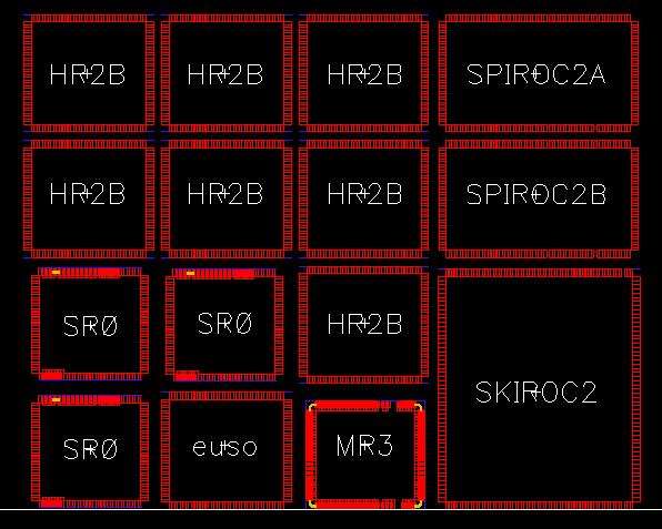
9.1 DHCAL technological prototype
9.1.1 HARDROC ASIC
The HARDROC readout is a semi-digital readout with three thresholds (2 bits readout) which allows both good tracking and coarse energy measurement, and also integrates on chip data storage. The chip integrates 64 channels of fast, low-impedance current preamplifiers with 6 bits variable gain (tuneable between 0 and 2), followed by a fast shaper (15 ns) and low offset discriminators. The discriminators feed a 128-deep digital memory to store the 2*64 discriminator outputs and bunch crossing identification coded over 24 bits counter. Each is then readout sequentially during the readout period.
A first version was been fabricated in AMS SiGe 0.35m technology in September 2006 and met design specifications. A second version was produced in June 2008 to fit in a smaller low-height package (TWFP160) which necessitated changing the double-row bonding pad ring into a single row, rerouting all of the inputs and removing many pads. A possibility for a third threshold was added at that time, also separating more widely the three thresholds (typically 0.1–1–10 pC) and the “off” power dissipation was brought down to a few W for the whole chip.
The trigger efficiency allows the MIPs for RPCs to be discriminated with 100 fC threshold (10 fC for Micromegas) with a noise of 1 fC (Fig. 47). The power pulsing scheme has also been validated, also shown in Fig. 47, where 25 s are required to start up the chip so that it can trigger on a 10 fC input signal. Finally the readout scheme, which is common to all the chips, has been validated on the large square-metre board, built as a scalable technological prototype of DHCAL that is read-out by the side.
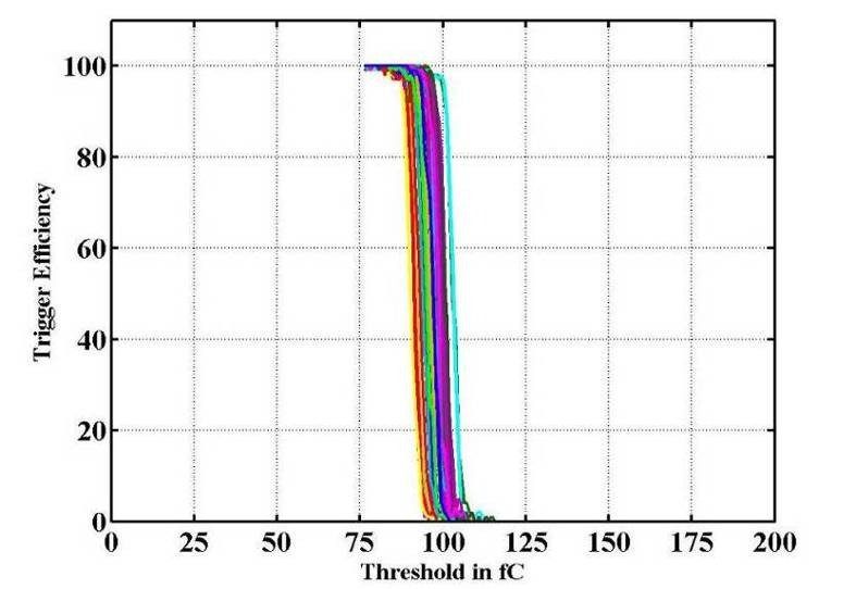
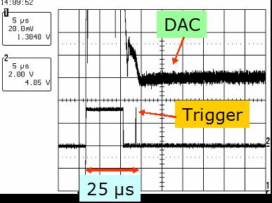
This HARDROC chip is the first one on which large scale power-pulsing has been tested at system level, allowing a power reduction by a factor of 100 while keeping the detector efficiency above 95%.
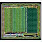
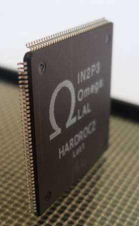
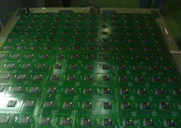
A production of 10 000 chips started in March 2010 to equip 40 GRPC planes of a one cubic metre detector that will be tested in 2011.
A specific test bench with a Robot, shown in Fig. 49, has been used at Lyon to test and qualify the chips before mounting them on the boards. The yield is about 93%.
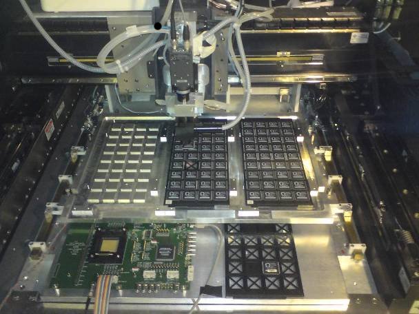
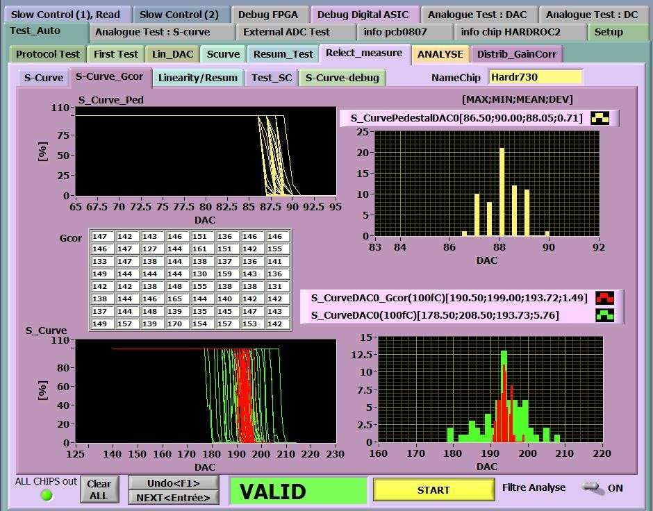
9.1.2 MICROROC ASIC
HARDROC has also been used in test beam to readout square metre Micromegas chambers. However, the required robustness to HV sparks and the abaility to detect signals down to 2 fC necessitate the design of a more sensitive version having a low noise charge preamplifier input stage. MICROROC is a 64 channel mixed-signal integrated circuit based on HARDROC, designed in AMS 350 nm SiGe technology (Fig. 50). Analogue blocks and the whole digital part are reused from HARDROC.
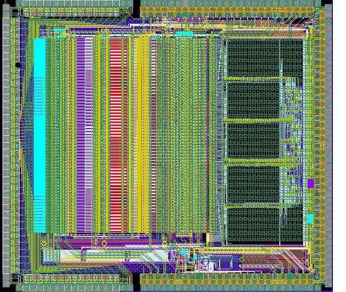
Each channel of the MICROROC chip is made of a very low noise fixed gain charge preamplifier optimised for a detector capacitance of 80 pF and able to handle a dynamic range from 1 fC to 500 fC, two different adjustable shapers, three comparators and a random access memory used as a digital buffer. All these blocks are power-pulsed, thus reaching a power consumption equal to zero in standby mode.
MICROROC has been tested on test bench and exhibits very good performance with in particular the ability to trigger down to 1 fC as shown in Fig. 51. 300 ASICs have just been packaged (TQFP160 plastic package) to equip and test two square metre Micromegas chambers.
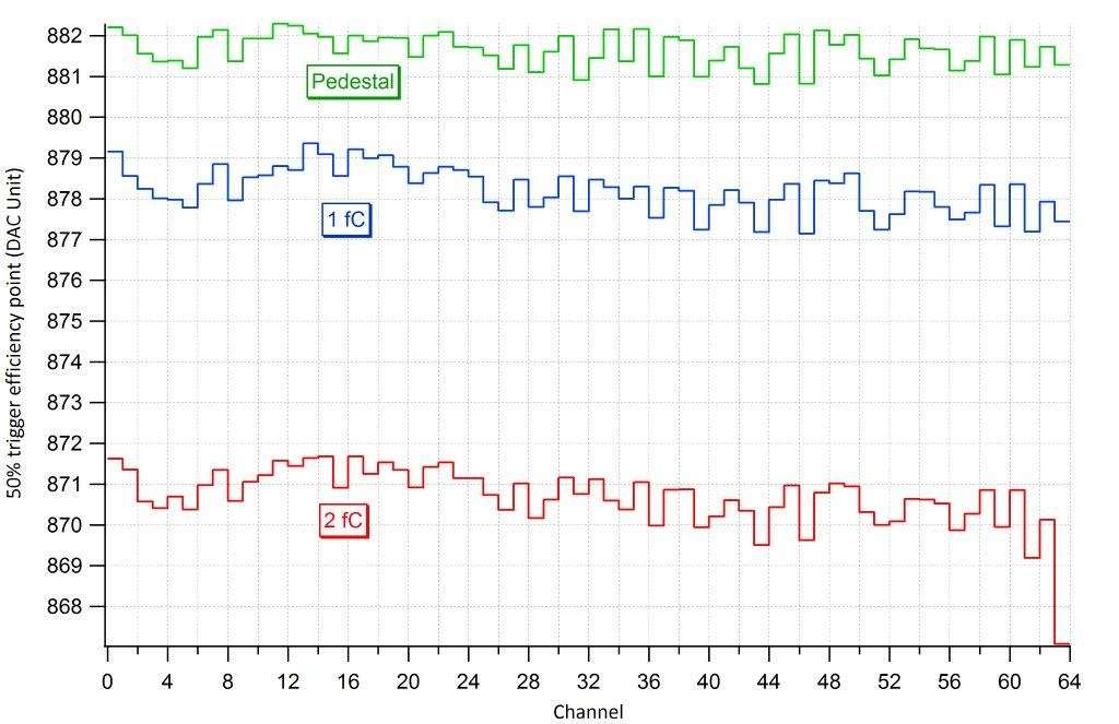
9.2 AHCAL technological prototype
The SPIROC ASIC that reads 36 SiPMs is an evolution of the FLC_SiPM used in the physics prototype. The first prototype was been fabricated in June 2007 in AMS SiGe 0.35m. and packaged in a CQFP240 package. Similarly to HARDROC, a second version, SPIROC2, was realized (Fig. 52) in June 2008 to accommodate a thinner TQFP208 package and fix a bug in the ADC.
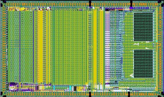
Each channel of SPIROC2 (Fig. 53) is made of:
-
An 8-bit input DAC with a very low power of 1W/channel as it is not power pulsed. The DAC also has the particularity of being powered with 5V whereas the rest of the chip is powered with 3.5V.
-
A high gain and a low gain preamp in parallel on each input allow handling the large dynamic range. A gain adjustment over 4 bits common for the 64 channels has been integrated in SPIROC2. A variant (SPIROC2B) with individual gain adjustment over 6 bits has also been produced.
-
The charge is measured on both gains by a “slow” shaper (50–150 ns) followed by an analogue memory with a depth of 16 capacitors.
-
The auto-trigger is taken on the high gain path with a high-gain fast shaper followed by a low offset discriminator. The discriminator output is used to generate the hold on the 36 channels. The threshold is common to the 36 channels, given by a 10 bit DAC similar to the one from HARDROC with a subsequent 4 bit fine tuning per channel.
-
The discriminator output is also used to store the value of a 300 ns ramp in a dedicated analogue memory to provide time information with an accuracy of 1 ns
-
A 12 bit Wilkinson ADC is used to digitize the data at the end of the acquisition period.
The digital part is complex as it must handle the SCA write and read pointers, the ADC conversion, the data storage in a RAM and the readout process.
The chip has been extensively tested by many groups. The first series of tests has been mostly devoted to characterizing the analog performance, which meets the design specifications. A single photoelectron spectrum using the full chain and a LED pulser is displayed in Fig. 54. The one photo-electron signal to noise ratio is around 8.
The linearity as a function of the input charge in the auto gain mode and using the internal ADC is shown in Fig. 55.
The digitization part has also been characterized and the 12 bit ADC exhibits a very good integral non-linearity of 1 LSB and a noise comprised between 0.5 and 1 LSB, as shown in Fig. 56.
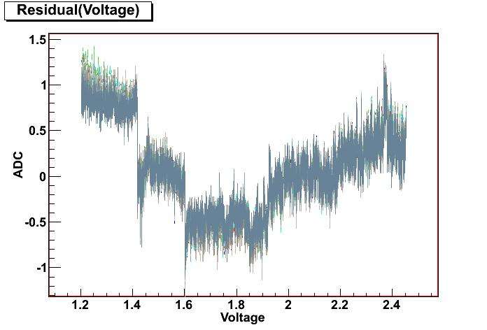
The chips have been assembled on a HCAL PCB (HBU) and tested with detector, as described in the HCAL section and are being operated with good results.
A new, improved version of the SPIROC-Chip with increased signal-to-noise ratio is currently being developed. For this a new frontend has been designed which provides higher signal-to-noise ratio at the same time retaining a large dynamic range. A first version of a test chip (KLauS 1.0) shows a signal-to-noise ratio of greater than ten for a signal charge of 40 fC. A second version (KLauS 2.0) including the power-pulsing option has been submitted end of 2010 and is presently tested.
9.3 ECAL technical prototype
For the ECAL, the chip SKIROC2 has been designed (Fig. 57) and submitted in the production run of March 2010. It keeps most of the analog part of SPIROC2, except for the preamp which is a low noise charge preamp followed by a low gain and a high gain slow shaper to handle a large dynamic range from 0.5 MIP ( fC) up to 2500 MIPs (10 pC).
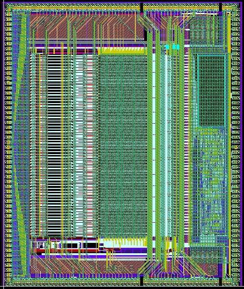
.
SKIROC2 chips are not packaged (except for test bench measurements) as they must be directly bonded on the printed circuits (Fig. 58). The characterization is performed on testbench using a few packaged chips but the produced chips will be tested using a probe station. FEV boards hosting 16 SKIROC2 chips are under design to readout 1024 channels.
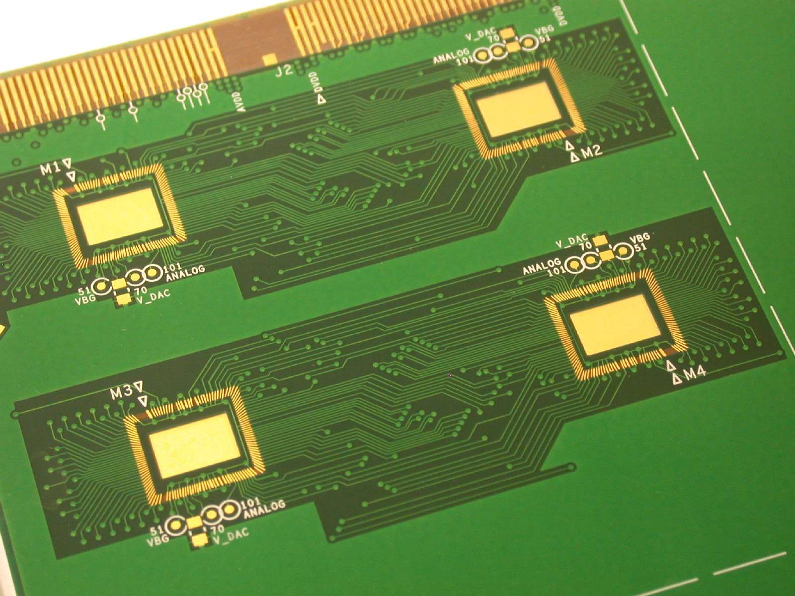
9.4 Conclusion
The second generation ASICs for CALICE/EUDET have been produced and a large quantity is therefore available to equip large scale detectors to check that all key issues have been solved. The design of the third and final generation where all channels are handled separately to allow higher zero-suppression has just begun in the AIDA framework.
10 Data Acquisition
A second version of the CALICE DAQ was proposed [32] within the framework of EUDET to read out the various technical prototypes being developed. The aim was to handle the many embedded readout chips and their direct digital output in test beams. A second goal was to serve as a prototype of techniques for the calorimeters of a large detector such as the ILD.
The project is now in the latest integration phase, prior to deployment in the CALICE labs. (DESY, IPNL, LAPP, LLR). Up-to-date information is kept on the CALICE Twiki DAQ pages [33] and regularly presented at CALICE meetings [34]. It has recently triggered interest of the FCAL Collaboration for a common interface, and will be part of the “common DAQ” package of the FP7 AIDA project, together with the telescope EUDAQ.
10.1 Functional specifications
All the technological prototypes feature embedded electronics in the form of ASICs with built-in memory situated in the detector volumes. This very front-end electronics performs analogue amplification and shaping, digitization, optionally internal triggering, and a local storage of data in memory. The various detectors share a commonly defined interface through custom Detector Interface (DIF) cards.
Two modes of operation are foreseen: a single event mode, in which the data readout is triggered by an external signal (typically in beam test operation), and an ILC-like mode which is consistent with that expected for the ILC beam structure, i.e. the readout of full train of data without external trigger, at a train frequency of Hz.
The DAQ should handle:
-
•
the loading of the configuration in the ASICs (seen as one stream of bits for one set of ASICs), and optionally the verification of the loaded data;
-
•
the management of the acquisition states trough commands: acquisition running mode [Single Event, ILC mode], StartReadout, StopReadout, Reset, Sync mode;
-
•
the distribution of the fast signals in a synchronous manner: Clock, Trigger and the collection and ORing of the busy signals the other way around. Synchronous here is detector and reconstruction specific: for the SDHCAL and ECAL a machine clock period (200 ns) should suffice, for the AHCAL the requirement is typically less than 1 ns;
-
•
the data flux, which are here reasonably low: for the SDHCAL, with an average of 4.8 HaRDROC chips with data per plane for a 100 GeV pion, an ASIC readout clock of 2.5 MHz, a data flux of the MB/s is expected in beam tests allowing for a maximum allowed event frequency of 3.2 kHz (much higher than the working region of standard GRPC, limited to a few 100 Hz for example). For the ECAL, equipped with 2 ASIC readout lines per DIF, 4 ASICs with data in each plane would generate a data flux of 113 MB/s for a maximum acquisition rate of 1.2 kHz. Under the same hypothesis as for the SDHCAL, the AHCAL data flux reaches 338 MB/s, allowing for a 4 kHz event rate. In all cases, the data flux is limited by the readout speed of the ASICs. A detailed table is available online [35].
-
•
two running modes: in single event mode, an external signal (typically signalling the passage of a particle of a given type, with a combination of scintillators and Cherenkov detectors) triggers a suspension of the acquisition mode of the ASIC, their readout and the resumption of the acquisition. In ILC-like mode, the ASICs are switched into Acquisition mode at the start of a particle spill, and are read out either at the end of the spill, after a given time span or number of particles, or when any of the detector ASICs emits a RAM-full signal. The acquisition is eventually resumed as soon as the readout is completed. As both modes use the auto-triggering capacity of the ASICs, they are very sensitive to noise. A careful online monitoring of the noise has to be performed, with an automatic correction procedure necessary to kill noisy channels.
10.2 Implementation
The overall scheme for the DAQ take the form a tree (see Fig. 59) with :
-
•
one (or more depending on data flux) DAQ PCs equipped with 1–2 ODR (Off Detector Receiver) card, or a standard Network card, linked via Optical or Electrical Gigabit Ethernet to 2–4 LDAs (Link Data Agregator) cards;
-
•
each LDA card services up to 10 connections to the DIFs (Detector InterFace card), or (case of the SDHCAL) to the DCC cards (Data Concentrator Card) via HDMI cables carrying all the needed signals.
-
–
each DCC is connected to up to 9 DIF cards (Detector InterFace);
-
–
-
•
each DIF manages a SLAB hosting many ROCs (Read-Out Chips) through one or several ASIC readout lines;
-
•
a CCC (Clock and Control Card) dispatches the fast signal to the DIFs via the LDAs & DCCs: external or internal clocks and Trigger/Sync signals. It collects the busy signals from the DIFs and blocks the external triggers accordingly. It can be controlled by the PC through an RS232 connection and provide simple logic and a 50 MHz clock.

Figure 59: DAQv2 scheme for the SDHCAL (with DCC cards ) and the ECAL (direct connection DIF–LDA)
All the data on the HDMI links are transferred using 8b/10b encoding for redundancy and passing of control signals.
The typical needs for the a complete SDHCAL (50 layers) set-up are of 150 DIFs, 17 DCCs, 2–3 LDAs; The ECAL requires 30 DIFs and 3–4 LDAs, the AHCAL 48 DIFs and 5–7 LDAs. Each system requires a CCC, and 1 ODR or Network card (2 for the AHCAL).
10.3 Planning & organisation
The design of the DAQv2 was developed by the CALICE UK groups (Cambridge, UCL, Manchester, RHUL) in the framework of EUDET. All the hardware developments were fulfilled by the UK institutes, with the exception of the DCC (LLR) and DIFs (DESY, LAPP, Cambridge). Starting in 2009, the funding support for ILC in UK dropped, resulting in the loss of expertise (engineers and postdocs leaving). The LLR group which was involved in the integration for the SDHCAL gradually took over the global integration and debugging tasks, while the IPNL group assumed responsibility for the development of the software framework.
A DIF Task force was set up in 2008, with one expert from each of LLR, LAPP, Cambridge and DESY, to establish a common interface and to coordinate the firmware development. All relevant documents and specifications (data exchange format, commands, etc.) are available [36].
10.4 Hardware availability
All the generic hardware elements (LDA and its mezzanine cards, DCC, CCC, ODR and PC) are ready and tested. A list of equipment is available [37]. By the end of 2010 most of the equipment was dispatched from the UK to the main testing labs (LLR, DESY, LAPP and IPNL).
The last physical parts produced in 2010 were the DCC and LDA cards; 20 DCC cards have been produced and been tested, with almost no failure found, they will be installed in a standard VME crate. The LDA are physically composed of a commercial baseboard, and 3 custom mezzanine cards respectively supporting the 10 HDMI connectors, the connection to the CCC and the Gigabit-Ethernet connection. After many difficulties with the company building the card (Enterpoint Ltd) and many delays, all the hardware parts are available; a mechanical structure is under study to host securely the CCC and the LDAs, both having non-standard formats, in the test beam area.
The HDMI cables’ specifications are determined by two requirements: for their length, by the physical arrangement of the detectors in the TB hall (4-5 m are needed), and for their composition, by safety requirements (Halogen free cables are mandatory for work in CERN). 150 cables are needed for the SDHCAL, another 30 for the ECAL, and 40 for the AHCAL. In total, 275 cables of 5 m length were manufactured specifically for the project and are being delivered: 100 cables are are available at LLR, the remainder are in transit. The first tests are fully satisfactory.
10.5 Firmware & implemented functionalities
The major occupation of the last year has concerned the firmware (FW) of all the cards.
First, a common FW for all DIF has been developed. A global framework was developed (LLR) for the interconnection of existing various parts; an 8b/10b decoding blocks (Manchester), testing modules (pseudo random pattern generation for high volume of data, and echo of configuration pattern), and working implementation of the ROC chips management used for the SDHCAL over USB (LAPP).
The DCC FW, including the 8b/10b parts and a multiplexing engine is complete and works as expected; the main objective here being its transparency.
The LDA FW has specifications very similar to the DCC, with the Downstream block being replaced by a Gigabit-Ethernet block. It is now 98% complete with only comfort functionality missing, such as a soft reset of the board, and a small instability of the incoming flux from the PC at full speed (this can easily be avoided by a small delay in the configuration sending).
Recent performance tests using pseudo-random data have shown the possibility to read up to 10 DIFs on 10 different DCC on one LDA or 10 DIFs on 1 LDA up to 32 MB/s almost without any failure (prelim. over 1 day) using an optical link, which is OK for the first use (20 MB/s for the SDHCAL).
The transfer of the Trigger and BUSY signal to the CCC has been much more problematic as expected due to the use of an AC coupling between the CCC and the LDA, leading to instabilities and stringer conditions on the length of the signals. Special treatment (conversion of continuous signal as clock) were implemented (UCL) and tested and improved (LLR). A furst working implementation was produced at the end of March 2011 and will still need more stringent tests.
Preliminary measurements of fast signals on DIFs connected to one full chain (CCC LDA DCC DIFs) has shown a clock jitter of 550 ps on a single DIF and a jitter of the trigger delay between 2 DIFs of 200 ps. This performance is acceptable for the most critical of the intended applications, namely the AHCAL readout.
The programming of the CCC CPLD has to be adapted for each setup (format of input signal, ORing and blocking logic) and will have to be performed; the FW code is fully available and expertise exits: for exampl LAPP have modified significantly the code to allow for a direct connection to the DIF implementing clock, trigger and (hard coded) fast command distribution to 3 DIFs [38].
10.6 Software
Some early development were done in the DOOCS framework, but were finally not pursued due to lack of manpower; in parallel, the XDAQ framework [39], used by IPNL for the readout of the first SDHCAL prototypes using a direct USB connection to the DIF, was also developed at IPNL to include most of the components necessary for the TB: event building, and online reconstruction via an interface to Marlin and root data quality histogram filling, an interactive GUI tool manage the acquisition and display histograms, the storage of RAW data in LCIO format.
This system has been working perfectly using the USB interface to the DIF for more than one year and is being used as part of a several month geological survey of a volcano near Clermont-Ferrand (by LPC colleagues), with almost no downtime. A stress test based on a LDA simulator injecting pseudo random data has shown stable performances up-to 500 MB/s.
The interface to the new hardware is now being finalised. Until recently, the basic chain PC+LDA+DCC+DIF has been mainly been tested at LLR using ad hoc SW elements based on python scripts & GUI and C libraries. In early January 2011, the C library was for the first time interfaced with the XDAQ environment as a driver and worked immediately, allowing for intensity data flow testing. The interface to the CCC is already done. A complete beta version of a C++ API for the LDA is now available and is ready to be integrated.
A first prototype of a configuration DB based on Oracle has been designed at IPNL, with a C++ API. In the near future, it will be validated and thoroughly tested. It is also foreseen to have a local file interface as a fallback solution for the scenario in which connectivity is lost.
A GUI is being developed in parallel to ease the use of the system for the low level electronics test in LLR.
10.7 Summary
The DAQ system is in good shape, without any obvious “show stoppers” on the horizon which could plausibly prevent it from being ready for cosmics data taking for the SDHCAL prior to test beam data (mid-June 2011). The other applications (ECAL and AHCAL) will follow easily. The emphasis has now to be put software, improvement of early online analysis (especially noise monitoring & correction) and testbeam interface.
11 Test Beam Analysis Results
The aims of the analysis of the test beam data are broadly twofold. Firstly, we wish to understand characterise the performance for these novel calorimeter designs, to assess their stability and to understand calibration issues. Secondly, we need to use these results to validate our Monte Carlo simulations, based on GEANT4 [40], which can then be used in the optimisation of global detector design. In particular, the simulation of hadronic showers is not theoretically well under control, especially at energies of a few GeV, characteristic of particles in jets. New experimental input is welcomed by the GEANT developers, some of whom are now members of CALICE.
11.1 Si-W ECAL performance
The Si-W ECAL was operated in the CERN beam tests in 2006-7, and in the first stage of the FNAL tests in 2008. It was exposed to beams of muons, electrons and hadrons. The muon data were used as the basis of detector calibration, so that recorded signals could be converted into minimum ionising particle (MIP) equivalents. The commissioning and calibration procedures have been described in some detail in [41]. First results on the response to electrons were published in [42]. More recent results [43] have explored the position and angular resolution of electron showers, with examples shown in Fig. 60. These results rely on a simple algorithm comparing the shower centroid reconstructed in the calorimeter with a track reconstructed in the upstream tracking chambers. The resolutions in (horizontal) and (vertical) are different because the sensor layers are staggered in .
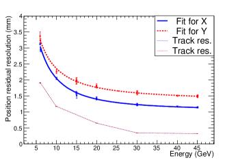
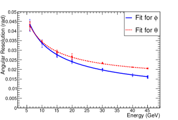
In a linear collider detector, some 50% of hadronic showers will start to develop in the ECAL, so it is of interest to study pion-induced showers in this detector. This allows us to probe the properties of showers in tungsten, and to exploit the high granularity of the ECAL to explore the properties of the first phase of the showers in unprecedented detail [44]. In Fig. 61 we show the energy-weighted mean shower radius in the ECAL as a function of pion energy, compared with the predictions of various physics lists in GEANT4. Most models underestimate the shower with, with the FTF models, based on the GEANT implementation of Fritjof, currently proving the most successful in version 4.9.3 of GEANT. The high segmentation of the ECAL allows the start of the shower to be identified with precision, and the small ratio of permits useful separation between three main components of the primary interaction — the nuclear fragments produced by spallation, the electromagnetic component and the MIP-like relativistic hadrons. This is illustrated in Fig. 62, taken from [44], which compares data with different physics lists. The contribution from short range spallation protons is clearly visible as the shoulder in the first few layers of the detector, a feature which none of the models manages to reproduce very well.
11.2 AHCAL performance
The completely instrumented AHCAL (described in section 5) was exposed to muon, electron and hadron beams in 2007-9, both with and without an ECAL in front. Muons were used for calibration. An important test of our understanding of the calorimeter is to check the response to positrons with no ECAL in front of the AHCAL [45]. The energy density in electromagnetic showers is particularly large, so this is a good test of the important SiPM saturation corrections, and other effects. Typical results are shown in Fig. 63. After saturation corrections are applied, satisfactory agreement between data and simulation is achieved, giving us confidence to proceed with the characterisation of hadronic showers.
Longitudinal profiles in the AHCAL have also been measured with respect to the shower starting point [46], and can be compared with Monte Carlo simulations broken down into their separate particle constituents, in a way similar to the ECAL analysis. In Fig. 64 we compare simulations to data at 8 GeV, and show ratios of Monte Carlo to data at three typical energies. In this case, the physics lists FTF_BIC and particularly QGSP_BERT seem to be the most successful at modelling data.
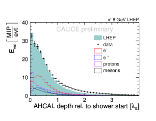
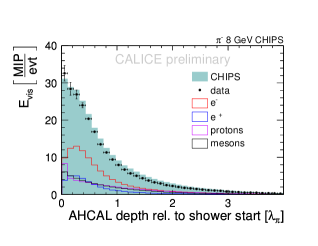
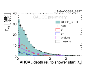
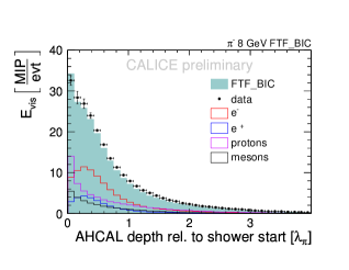
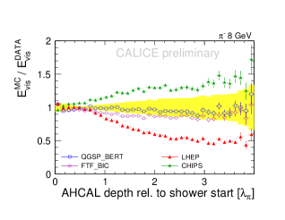
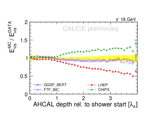
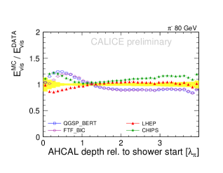
The CALICE calorimeters are non-compensating, i.e. their response ratio is not unity, and hence the hadronic energy resolution is affected by the fluctuations in the electromagnetic energy fraction in showers. However, the high granularity of the calorimeters permits significant pattern recognition within showers, allowing some possibility of disentangling the components and weighting them differently (a procedure known as software compensation. Several studies along these lines have been carried out exploring different techniques [47, 48, 49]. The basic idea in all these approaches is that the electromagnetic parts of showers have greater energy density, so that hits of high energy, or in regions of high energy density, are weighted differently. An example of the results is shown in Fig. 65, taken from [48], and typical of all the studies. It is found that the energy resolution can be improved by typically 15-20%, achieving a stochastic term in the range 45-50%/. In addition, the linearity of the response is improved.
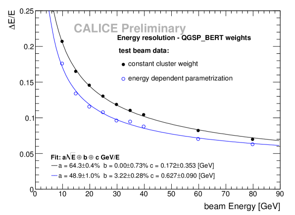
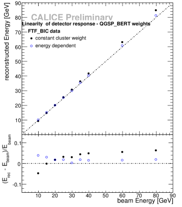
The high segmentation of the calorimeters also permits the identification of MIP-like track segments within hadronic showers. This has been studied in detail using the AHCAL in [50]. As well as providing a useful way of monitoring the calibration of the tiles, the study of these track segments permits novel tests of shower simulation models. For example, in Fig. 66 we show the total track length and the number of separate segments in pion-induced showers, compared with GEANT4. We note that none of the physics lists is notably successful in modelling this aspect of the data.
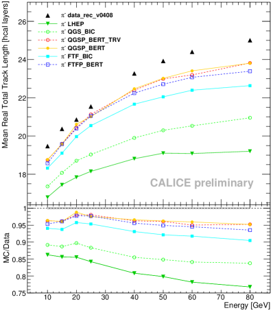
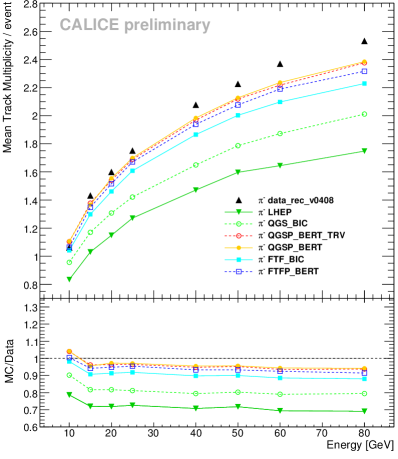
11.3 Combined calorimeter system
The CALICE beam tests included data taken with a full system of Si-W ECAL, AHCAL and tail catcher (TCMT), in order to emulate the behaviour of a full linear collider calorimeter system. In one of the studies of software compensation cited above [47], the same approach were applied to showers the full system of ECAL, HCAL and TCMT, and the improvement in performance was just as good as for the HCAL alone.
One of the main motivating forces behind the CALICE program has been to optimise the calorimetry for particle flow reconstruction of jets. It is therefore of obvious interest to use the test beam data in ways which directly test the features used in existing particle flow algorithms, such as Pandora-PFA [51], which is currently regarded as the state-of-the-art program. In a PFA, the calorimeter is used to measure the energy of neutral particles, and the HCAL particularly for neutral hadrons. An important issue is the degree of “confusion”, i.e. the extent to which the energy measurement of a neutral particle may be degraded by the presence of nearby charged particles.
A first such test has been presented in [52], in which a configuration consisting of a charged pion close to a neutral hadron shower is emulated. This is done by
superimposing two test beam pion-induced events, removing the incoming MIP-like track segment from one in order to emulate the neutral hadron. These events can be overlaid using various transverse displacements, and are then presented to Pandora-PFA for reconstruction and the fidelity of the recovery of the energy of the neutral is examined. A comparison with the measured energy before overlaying is the used to assess the degree of confusion. In Fig. 67 we show the average difference between measured and recovered energy and its r.m.s. as a function of the shower separation, for two typical energies. The data are compared with GEANT4 simulations using different physics lists. We see that the simulation, especially using the QGSP_BERT model, gives a reasonably faithful description of data, suggesting that the performance found for PandoraPFA in [51] is quite reliable.
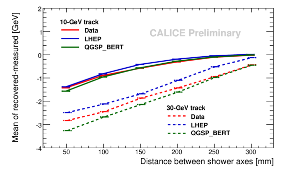
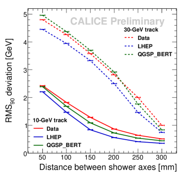
11.4 Sc-W ECAL performance
A good energy resolution performance for electrons as well as a reasonable linearity was presented in the previous report, an example being shown in Fig. 68. As part of these tests, we introduced a target into the charged pion beam line at FNAL to produce neutral pions, and reconstructed the invariant mass distribution of the detected photon pairs, as shown also in Fig. 68.
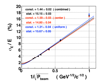
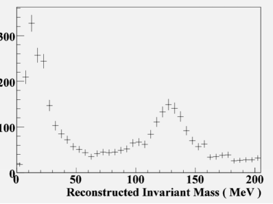
11.5 DHCAL performance
The 1 m3 DHCAL prototype had its first test beam run at Fermilab in late 2010, exposed to beams of positrons, muons and pions. First results were recently presented. Clean muon tracks have been seen, and used to assess the efficiency of the RPCs and the pad multiplicity associated with single MIP hits. Extensive studies of the noise performance have also been shown. A start has also been made on the analysis of positron and pion shower data. Data were collected at various momenta between 2 and 60 GeV/c. The content of positrons in the beam varies from dominating at 2 to negligible at 60 GeV/c. First results on the response and resolution of the detector are then obtained by using the number of hits as a measure of energy. A preliminary analysis of the data showed the expected response for both pions and positrons. As an example, Fig. 69 shows the response (number of hits) for 20 GeV/c pions and positrons. Fig. 70, taken from [22], shows the response of the calorimeter (as measured by the number of hits) to pions and the fractional resolution (estimated using the r.m.s.). The response is seen to be well proportional to energy up to 24 GeV, with signs of non-linearity appearing at 32 GeV. The resolution based on this relatively simple analysis behaves in the expected way with energy. Clearly this calorimeter provides a great detailed information about the internal structure of the shower, which will permit improvements using software compensation techniques in a similar way to the analogue calorimeters.
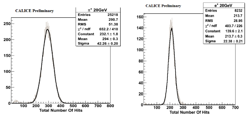
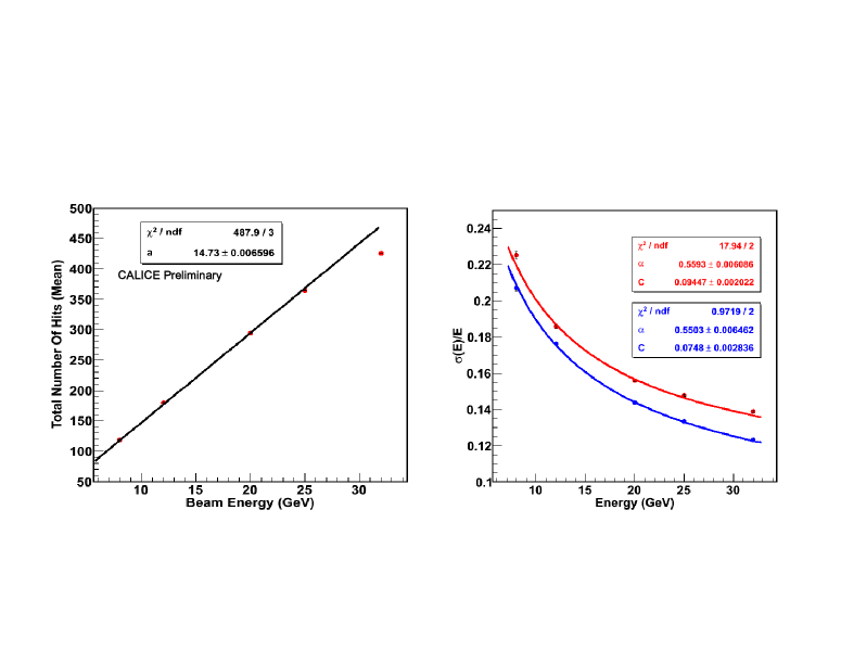
11.6 WHCAL and T3B results
For a detector at CLIC energies, a tungsten-based HCAL is attractive because of its density. The thickness of the HCAL needs to be thick, and the cost of immersing such a calorimeter in the magnet coil seems prohibitive if it was made of iron. However, there is little experimental understanding of the characteristics of hadronic showers in tungsten, which could be quite different from iron; for example more energy will be expended on nuclear spallation, because of the large atomic weight. It is therefore imporatant to validate GEANT4 for such a device. For this reason, the CALICE AHCAL tile detectors have recently been tested using tungsten absorber plates in a CERN test beam, as described in Sect. 6. Analysis of the results is at an early stage, but present indications are that:
-
•
The hadronic shower signals from pions and protons are comparable to the ones observed with an iron absorber.
-
•
The electromagnetic resolution seems to be slightly worse than with the iron absorber reflecting the lower sampling ratio with respect to
-
•
The ratio seems to be stable versus energy
As described in Sect. 6.3, the T3B module was introduced for these tests in order to explore the time structure of the showers. A measure which provides a good indication of the intrinsic time stamping possibilities in the calorimeter is the time when a cell which contains energy in a given event is first hit. In a first analysis of the T3B data, this was determined from the decomposed waveforms. Here, signals with an amplitude equivalent of at least 0.4 MIP within 9.6 ns were considered. The time of first hit was determined from the second photon detected within the selected 9.6 ns period (the second photon was used to reduce the impact of background from dark noise). The same quantity was determined in simulations of T3B with a description of the complete detector setup, including a parametric smearing of the arrival time of photons on the SiPM to account for the response of the scintillator and for photon travel times. Simulations were performed with two different Geant4 physics lists, QGSP_BERT and QGSP_BERT_HP. The latter includes high precision neutron tracking.
To provide first robust comparisons between data and simulations, the mean time of first hit for each of the T3B cells was determined from the distribution of the first hit. The mean was formed within a time window of 200 ns, starting 10 ns before the maximum of the distribution in T3B tile 0, and extending to 190 ns after the maximum. This time window covers the time relevant for calorimetry at CLIC, where the duration for one bunch train is expected to be 156 ns, and is also comparable to the shaping time of 180 ns used in the front end electronics of the CALICE analog HCAL modules.
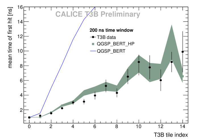
Figure 71 shows the mean time of first hit as a function of the radial distance from the shower axis. The beam axis passes through T3B tile 0, so that a tile index of 10 corresponds to a distance of approximately 30 cm. The measurement is compared to the simulations with the two physics lists, QGSP_BERT and QGSP_BERT_HP. While QGSP_BERT_HP gives an excellent description of the data, QGSP_BERT shows very large discrepancies, with significantly overestimated late contributions at larger radii. This demonstrates the importance of the high precision neutron tracking in Geant4 for a realistic reproduction of the time evolution of hadronic showers in tungsten.
Further measurements at higher energies, measurements with steel absorbers and an extension of the data analysis and of the simulation studies are in preparation.
11.7 Effects of high-energy particle showers on the embedded front-end electronics
As indicated above, the second generation calorimeter prototypes will have the readout electronics embedded into the active layers of the calorimeter. The energy of electromagnetic showers produced in the final states of collisions at a future lepton collider ranges between a few MeV up to several hundreds of GeV. A natural question arising from this design is whether the cascade particles of the high-energy showers which penetrate through the electronics would create radiation induced effects in these circuits. A series of test runs has been performed and analysed in order to prove the feasibility of having embedded readout electronics for the calorimeters. In these runs an ordinary calorimeter layer of the physics prototype for the silicon tungsten electromagnetic calorimeter, see Section 2, has been replaced by a special PCB allowing for the exposure of the readout electronics to particle showers. A detailed analysis of noise spectra of the ASICs exposed to high-energy electron beams gives no evidence that the noise pattern is altered under the influence of the electromagnetic showers. As shown in Figure 72, the probability for a faked signal is less than for thresholds larger than 1/2 of a MIP where the MIP level is defined to be around 45 ADC counts, see also [41]. The probability to have faked signals above the MIP level is estimated to be smaller than . The analysis is published in [53].
For an event of the type at at the lepton collider about 2500 cells of dimension are expected to carry a signal above noise level which is typically defined to be (60-70)% of a MIP. The presented results revealed no problems for the design of embedded readout electronics. It is furthermore unlikely that the residual deviations between the observed number of hits and those expected from normal noise fluctuations can be attributed to the influence of the beam but rather to an imperfect modelling of the noise spectra for signal events. In this sense, the presented results constitute a conservative upper limit.
12 Future Beam Test Plans
Beam tests a naturally vital for the success of R&D of the detectors. Beside its large generic approach, the CALICE efforts are targeted towards the Baseline Design Document for ILC detectors, to be delivered until the end of 2012, and the Conceptual Design Report for CLIC detectors to be delivered until the end of 2011. The planning of beam test times is therefore very much focussed on data taking during 2011 and 2012. This is particular true for those technologies who are supposed to be considered as base line of the detector concepts. The beam test plans for the next years are summarised in Table 3.
12.1 Physics prototypes
The year 2011 sees the finalisation of the main physics prototype phase. The physics prototype of the DHCAL based on RPCs has been completed in the first half of 2010 and conducted two successful beam test campaigns of four weeks each in October 2010 and January 2011. In the beam test period of October 2010 the rear part of the DHCAL stack was completed with the scintillator based TCMT while in January 2011 the scintillator layers were replaced by RPCs. During April 2011 there is data taking in combination with the Si-W ECAL. The physics program to be conducted will be largely oriented on that which has been done in the corresponding data taking in the years 2006-09. During 2011 small units of GEM chambers will be tested. The tests of 1 chambers is planned to start around 2013.
The scintillator layers of the physics prototype of the analogue Hcal serve as sensitive devices for a physics prototype with tungsten as absorber material. Tungsten is the most probable absorber for a hadron calorimeter for CLIC detectors. A first data taking has been realised in autumn 2010 with low energy pions. The plan for 2011 is to extend the energy range to energies of several 100 GeV as relevant for detectors at CLIC. Originally, 8 weeks of data taking at the SPS have been required from CERN. However, due to the high demand on the CERN beam lines and the priority to assign test beam time for LHC upgrade project, the assigned beam time by CERN will be considerably shorter. This clearly puts in jeopardy the physics goals of the test beam. It has to be seen to what extent the loss of beam time in 2011 can be recovered in 2012. This is also true for other projects described below.
Due to funding problems there are currently no beam test plans for the DECAL.
12.2 Technical prototypes
The previous sections indicate that the CALICE collaboration is entering a new phase of R&D in which readout technologies and mechanical designs already meet many requirements of operation in a detector for a linear collider.
It has to be stressed that the primary goal of these prototypes is to study technological solutions for the calorimetry at a future lepton collider. The strategy for the coming years should take this into account. Here the main keywords are power pulsing and the limited depth of the buffers in the VFE which may require consideration of the time structure of the beams. In addition to the purely technological issues a physics program is to be pursued. This physics program is derived from those of the physics prototypes, taking the new technical constraints into account. It requires the operators of testbeam sites to actively respond to the needs of the CALICE (LC) testbeam data taking at an very early stage.
Two campaigns of large scale test beams with a fully equipped 1 technical prototype of an SDHCAL equipped with GRPCs will be conducted during 2011 at CERN. As for the SDHCAL the original plan of about 8 weeks of running time has been severely cut down as indicated above.
Beyond these large scale tests, beam tests with smaller units will be conducted. Namely, these test beam efforts comprise:
-
•
Testbeams in 2011 with 1 units of the technical prototype of the SDHCAL with Micromegas. These test will be conducted at CERN.
-
•
The analogue hadron calorimeter will progressively equip the device with scintillating tiles and read out electronics. The intermediate goal is to realise a so called vertical test towards the end of 2011 or the beginning of 2012. This means the available equipment will be arranged to allow for the measurement of electromagnetic showers.
-
•
The Si-W ECAL is planning to make tests with single ASU towards the middle of 2011 in an electron testbeam. The detector will be progressively equipped with ASUs to allow for larger beam test towards the end of 2012. This test may be conducted together with the 1 of the SDHCAL. Tests are to be conducted at CERN, DESY or, if beam availability requires, at FNAL.
-
•
The Scint-W ECAL is planning to make tests with single ASU towards the middle of 2011 in an electron test beam. This project will benefit from the existing infrastructure for the SiW Ecal as well as from the integrated approach on front electronics and DAQ as pursued within CALICE.
It is envisaged to have a combined running of the SiW Ecal technological prototype with the GRPC SDHCAL. The time line for this is unclear as the SiW Ecal is still going through small unit tests. In addition a number of technical questions (PCB planarity, wafer technology) need to be answerd before the start of the production of a full size prototype. Primarily these combined tests are to be conducted at CERN. The planning of the combined test needs to take into account that the CERN beam lines will be shut down during 2013 and 2014. An alternative would be to go Fermilab which however would require significantly more funding. In general the CALICE collaboration will also consider the option to use the new ESTB beam line at SLAC. Whether this beam line serves the CALICE needs is however not clear at the moment.
The running of an AHCAL technical prototype alone and together with the Si-W ECAL technical prototype is planned as well but depends also on the detector readiness. Here, also the times lines of the AHCAL have to be taken into account. Therefore no plans for beam test times and locations can be given at this moment.
In any case, during the year 2011, mechanical interfaces between the different detector types will have to be defined. In general terms the realisation of a combined running is already prepared now as the DAQ system is common for all three calorimeter types. It can be expected that this DAQ system becomes fully operational during the year 2011.
| Project | 2011/1 | 2011/2 | 2012/1 | 2012/2 | 2013/1 | 2013/2 |
|---|---|---|---|---|---|---|
| Si-W ECAL/DCHAL RPC/TCMT () | xx | xx | xx | ? | ? | ? |
| DHCAL GEM (, ) | - | x | x | x | x | x |
| W HCAL / TCMT () | xx | xx | xx | ? | ? | ? |
| GRPC SDHCAL () | xx | xx | xx | xx | ? | ? |
| Mmegas SDHCAL () | x | x | x | x | ? | ? |
| AHCAL () | x | x | x | x | ? | ? |
| Si-W ECAL () | - | x | x | xx | ? | ? |
| Sc-W ECAL () | - | x | x | x | ? | ? |
12.3 Concluding remarks on test beams
A critical point is the availability of beam time. While at FNAL sufficient time could have been allocated in 2011, the request for CERN was, despite a good preparation and a favourable evaluation by the CERN SPS committee, severely downscaled. We would like to ask the DESY PRC to take note of this fact which might reduce proportionally the results to be expected particularly until the end of 2012. Unfortunately, the high availability of the DESY test beam remedies the situation only by a little as most of the prototypes require high energy hadrons which after all are the largest experimental challenge for calorimeters at future linear colliders.
It needs to be stressed as well that the time plans presented here depend essentially on the available funding to complete the various prototypes. Thus, the actual running of, in particular, the test beams with fully equipped prototypes could easily be delayed by one year with respect to the dates indicated in Table 3.
13 Summary and Outlook
The first phase of the CALICE program, the test series of physics prototypes, is nearing completion. The silicon and scintillator based tungsten ECALs and the scintillator HCAL perform as expected, and the first encouraging results from the gaseous HCAL point into the same direction. Test beam data provide detailed feedback for the refinement of simulation models, and with the successful application of the PANDORA algorithm to real data the high granularity approach to calorimetry has been validated. The data presently being taken at Fermilab will for the first time allow us to assess the potential of digital calorimetry on a firm experimental basis.
At the same time, the second generation of highly integrated scalable prototypes enters the production phase. Power pulsing in magnetic fields and operation of the mixed circuit ASICs in dense high energy electromagnetic showers have been tested successfully in beam. With the recent advancements in front end electronics and DAQ, all components are in hand for the various ECAL and HCAL technologies, and the semi-digital HCAL will pioneer the system integration and large scale tests.
The multi-TeV range poses its own challenges in terms of detector density and speed. Tungsten as an absorber material is being explored with scintillator as active medium, tests with gas are aimed at and technically possible in 2012.
In view of the timeline of the ILC technical design report and detector baseline documents, we expect to reach the most important goals:
-
•
Studies of performance, and comparisons with Geant 4 simulations, of physics prototypes for four major technologies, the silicon and scintillator ECAL, and the scintillator and gas HCAL. All relevant ECAL HCAL combinations have been tested together in joint set-ups.
-
•
A large scale system test of second generation gaseous HCAL with power-pulsed electronics, and an experimental test of the semi-digital method for an RPC HCAL.
-
•
Demonstrator tests, at least at single layer or single slab level, of the electronics integration concept for scalable prototypes of silicon and scintillator ECAL and scintillator HCAL, as well as HCALs with alternative gaseous readout (GEMs, micromegas)
In 2012, the detector concept groups ILD and SiD are asked to establish baseline technologies for the different sub-detectors. Studies of the overall physics performance, e.g. in conjunction with the tracking systems, or the integration into the overall detector engineering concept are beyond the scope of the CALICE program and need to be addressed in the context of the individual concepts. Based on the expected results above, CALICE foresees an assessment of the readiness of the different options on the technological level, and in matters of generic calorimetry. A number of criteria will be evaluated:
-
•
Established performance: energy resolution, linearity, uniformity, two particle separation
-
•
Validated simulation: longitudinal and transverse shower profiles, response, linearity and resolution, for electrons and hadrons
-
•
Operational experience: dead channels, noise, stability, monitoring and calibration
-
•
Scalable technology solutions: power and heat reduction, low volume interfaces, data reduction, mechanical structures, dead spaces, services and supplies
-
•
Open R&D issues: analysis and R&D to be completed before a first pre/production prototype can be built, cost reduction and industrialization issues
We expect that, due to resource limitations, not for all issues and all technologies the information will be as complete as might be desirable and as was the goal after the LOI. Therefore, a consensual assessment of the open issues is essential for the formulation of a coherent R&D program for the time after 2012.
In order to further proceed towards realistic detector proposals, the prototypes presently under construction should be extended to full module scale. The integrated electronics and associated heat dissipation, but also the on-detector zero suppression represent operational challenges which go beyond that of the first generation detectors, and performance must be re-established at large scale, including new monitoring and correction procedures. In addition, each of them offers added physics value for the study of hadronic showers and their reconstruction:
-
•
The ECAL will have four times finer segmentation.
-
•
The AHCAL has time-resolving electronics for the study of shower evolution in time and suppression of delayed neutron response.
-
•
The SDHCAL combines fine segmentation with some amplitude information and should continue to take data with different absorbers, and in combination with the new ECAL.
These issues constitute the logical next steps and need to be addressed for any future high granularity calorimeter, and the results will continue to advance our understnding of shower physics and calorimetry in general.
Consequently we expect a continuing demand for extensive test beam running. In the past, our requests have been fulfilled only with compromises, and the response to our needs in the particularly intensive period towards 2012 has been plainly inadequate. Too restricted access to beam time is one of our main concerns at present and jeopardizes the timely return on the investments made into the prototypes.
We request the PRC to endorse our planning towards 2012, to acknowledge the importance and relevance of a continuation of the studies beyond that date, and finallly to back up our test beam requests.
14 Acknowledgments
We would like to thank the technicians and the engineers who contributed to the design and construction of the prototypes. We also gratefully acknowledge the DESY, CERN and FNAL managements for their support and hospitality, and their accelerator staff for the reliable and efficient beam operation.
We would like to thank the HEP group of the University of Tsukuba for the loan of drift chambers for the DESY test beam. The authors would like to thank the RIMST (Zelenograd) group for their help and sensors manufacturing. This work was supported by the Bundesministerium für Bildung und Forschung, Germany; by the the DFG cluster of excellence ‘Origin and Structure of the Universe’ of Germany ; by the Helmholtz-Nachwuchsgruppen grant VH-NG-206; by the BMBF, grant no. 05H09VHG; by the Alexander von Humboldt Foundation (Research Award IV, RUS1066839 GSA); grant HRJRG-002, Russian Agency for Atomic Energy, ISTC grant 3090; by Russian Grants SS-1329.2008.2 and RFBR0402/17307a and by the Russian Ministry of Education and Science; by MICINN and CPAN, Spain; by CRI(MST) of MOST/KOSEF in Korea; by the US Department of Energy and the US National Science Foundation; by the Ministry of Education, Youth and Sports of the Czech Republic under the projects AV0 Z3407391, AV0 Z10100502, LC527 and LA09042 and by the Grant Agency of the Czech Republic under the project 202/05/0653; and by the Science and Technology Facilities Council, UK.
References
-
[1]
P. Sicho et al..
A large scale prototype for a SiW electromagnetic calorimeter for a future linear collider - EUDET Module.
http://www.eudet.org/e26/e28/e86887/e104848/EUDET-Memo-2010-17.pdf - [2] SPiDeR Collaboration, N.K. Watson et al., DESY PRC Report, Oct 2009.
- [3] Paul Dauncey, Performance of CMOS Sensors for a digital electromagnetic calorimeter, Proc. 35th International Conference on High Energy Physics, July 22–28 2010, Paris, France.
- [4] J.A. Ballin em et al., Design and performance of a CMOS study sensor for a binary readout electromagnetic calorimeter, arXiv:1103.4265v2 [physics.ins-det], submitted to JINST.
- [5] K.Gadow, E.Garutti, P.Göttlicher et al., JRA3 Hadronic Calorimeter Technical Design Report, Eudet-Memo-2008-02, http://www.eudet.org/e26/e28/e615/e626/eudet-memo-2008-02.pdf.
-
[6]
K.
,Gadow, P. Göttlicher, K.Kschioneck, M.Reinecke, F.Sefkow, HCAL mechanical design and electronics integration, Eudet-Memo-2008-23, http://www.eudet.org/e26/e28/e615/e866/EUDET-Memo-2008-23.doc - [7] C. Adloff et al., Construction and commissioning of the CALICE analog hadron calorimeter prototype, \jinst52011P05004.
- [8] I. Polák, An LED calibration system for the CALICE HCAL, to be published in Proc. IEEE Nuclear Science Symposium (NSS10), Knoxville, Tennessee, USA, Nov. 2010.
- [9] R. Fabbri for the CALICE Collaboration, CALICE Second Generation AHCAL Developments, Proc. 2010 LCWS, arXiv:1007.2358v1 [physics.ins-det].
- [10] J. Rouëné, Analysis of the autotrigger of the read out chip of the front-end electronics for the HCAL of the ILC, unpublished summer student report, June 2010, http://www.desy.de/f/students/2010/reports/rouene.pdf
- [11] First T3B Results - Initial Study of the Time of First Hit in a Scintillator-Tungsten HCAL, CALICE Analysis Note CAN-033, https://twiki.cern.ch/twiki/pub/CALICE/CaliceAnalysisNotes/CAN-033.pdf.
- [12] F. Simon, C. Soldner, Uniformity Studies of Scintillator Tiles directly coupled to SiPMs for Imaging Calorimetry, doi:10.1016/j.nima.2010.03.14, Nucl. Instrum. Meth. A620 (196) 2010.
- [13] G. Drake et al., doi:10.1016/j.nima.2007.04.160, Nucl. Instrum. Meth. A578 (88) 2007.
- [14] B. Bilki et al., \jinst32008P05001.
- [15] B. Bilki et al., \jinst42009P04006.
- [16] B. Bilki et al., \jinst42009P10008.
- [17] B. Bilki et al., \jinst42009P06003.
- [18] Q. Zhang et al., \jinst52010P02007.
- [19] http://www.hep.anl.gov/repond/DHCAL.html
-
[20]
CALICE DHCAL Noise Analysis, CALICE Analysis Note CAN-031,
https://twiki.cern.ch/twiki/pub/CALICE/CaliceAnalysisNotes/CAN-031.pdf. -
[21]
Analysis of DHCAL Muon Data, CALICE Analysis Note CAN-030,
https://twiki.cern.ch/twiki/pub/CALICE/CaliceAnalysisNotes/CAN-030.pdf. -
[22]
DCHAL Response to Positrons and Pions, CALICE Analysis Note CAN-032,
https://twiki.cern.ch/twiki/pub/CALICE/CaliceAnalysisNotes/CAN-032.pdf. - [23] ILD Concept Group, The International Large Detector - Letter of Intent, DESY-09-087, arXiv:1006.3396 [hep-ex].
- [24] Yue Qian et al., Measurement of avalanche size and position resolution of RPCs with different surfaces resistivities of the high voltage provider, 2010 Chinese Phys. C 34 565 doi: 10.1088/1674-1137/34/5/010
- [25] M. Bedjidian et al., Performance of Glass Resistive Plate Chambers for a high granularity semi-digital calorimeter, \jinst62011P02001.
- [26] M. Bedjidian et al., Glass resistive plate chambers for a semi-digital HCAL, doi:10.1016/j.nima.2010.02.168, Nucl. Instrum. Meth. A623 (1) 120
- [27] C. Adloff et al., MICROMEGAS chambers for hadronic calorimetry at a future linear collider, \jinst42009P11023.
- [28] C. Adloff et al., Beam test of a small MICROMEGAS DHCAL prototype, \jinst52010P01013.
- [29] C. Adloff et al., MICROMEGAS Test Beam 2008 - Analysis & Results, 2009, LAPP-TECH-2009-04, HCAL: in2p3-00413881.
- [30] C. Adloff et al., Environmental study of a Micromegas detector, 2009, LAPP-TECH-2009-03, HCAL: in2p3-00544969.
- [31] C. Adloff et al., A MICROMEGAS chamber with embedded DIRAC ASIC for hadronic, \jinst42009P11011.
- [32] M. Wing, M. Warren, P.D. Dauncey, J.M. Butterworth, A proposed DAQ system for a calorimeter at the International Linear Collider, arXiv:0611299v1 [physics.ins-det].
- [33] https://twiki.cern.ch/twiki/bin/view/CALICE/CALICEDAQ.
- [34] http://ilcagenda.linearcollider.org/categoryDisplay.py?categId=154.
- [35] https://twiki.cern.ch/twiki/bin/view/CALICE/DaqPerfs.
- [36] https://twiki.cern.ch/twiki/bin/view/CALICE/DetectorInterface.
- [37] https://twiki.cern.ch/twiki/bin/view/CALICE/HardwareList.
- [38] J.\,Prast,presentationhttp://ilcagenda.linearcollider.org/conferenceDisplay.py?confId=4391.
- [39] https://svnweb.cern.ch/trac/cmsos.
-
[40]
S. Agostinelli et al., doi:10.1016/S0168-9002(03)01368-8, Nucl. Instrum. Meth. A506 (2003) 250;
J.Allison et al., IEEE Transactions on Nuclear Science 53 No. 1 (2006) 270. - [41] J. Repond et al., Design and Electronics Commissioning of the Physics Prototype of a Si-W Electromagnetic Calorimeter for the International Linear Collider, \jinst32008P08001.
- [42] C. Adloff et al., Response of the CALICE Si-W Electromagnetic Calorimeter Physics Prototype to Electrons, doi:10.1016/j.nima.2009.07.026, Nucl. Instrum. Meth. A608 (2009) 372.
- [43] Study of position and angular resolution for electron showers measured with the electromagnetic SiW prototype, CALICE Analysis Note CAN-017, https://twiki.cern.ch/twiki/pub/CALICE/CaliceAnalysisNotes/CAN-017.pdf.
- [44] J. Repond et al., Study of the interactions of pions in the CALICE silicon-tungsten calorimeter prototype, \jinst52010P05007.
- [45] J. Repond et al., Electromagnetic response of a highly granular hadronic calorimeter, \jinst62011P04003
- [46] Pion Showers in the CALICE AHCAL, CALICE Analysis Note CAN-026, https://twiki.cern.ch/twiki/pub/CALICE/CaliceAnalysisNotes/CAN-026.pdf.
- [47] Initial Study of Hadronic Energy Resolution in the Analog HCAL and the Complete CALICE Setup, CALICE Analysis Note CAN-015, https://twiki.cern.ch/twiki/pub/CALICE/CaliceAnalysisNotes/CAN-015.pdf.
- [48] Software Compensation for Hadronic Showers in the CALICE AHCAL and Tail Catcher with Cluster-based Methods, CALICE Analysis Note CAN-021, https://twiki.cern.ch/twiki/pub/CALICE/CaliceAnalysisNotes/CAN-021.pdf.
- [49] A new approach to software compensation for the CALICE AHCAL, CALICE Analysis Note CAN-028, https://twiki.cern.ch/twiki/pub/CALICE/CaliceAnalysisNotes/CAN-026.pdf.
- [50] Identification of Track Segments in Hadronic Showers in the Analog Hadron Calorimeter - Algorithm and Comparisons to Simulations, CALICE Analysis Note CAN-022, https://twiki.cern.ch/twiki/pub/CALICE/CaliceAnalysisNotes/CAN-022.pdf.
- [51] Particle Flow Calorimetry and PandoraPFA algorithm, M.A. Thomson, doi:10.1016/j.nima.2009.09.009, Nucl. Instrum. Meth. A611 (2009) 25.
- [52] PandoraPFA tests using overlaid charged pion test beam data, CALICE Analysis Note CAN-024, https://twiki.cern.ch/twiki/pub/CALICE/CaliceAnalysisNotes/CAN-024.pdf.
- [53] J.Repond et al., “Effects of high-energy particle showers on the embedded front-end electronics of an electromagnetic calorimeter for a future lepton collider”, arXiv:1102.3454v3 [physics.ins-det], accepted by NIM, NIMA53658, doi: 10.1016/j.nima.2011.06.056.