A new experimental approach for the exploration of topological quantum phenomena
Abstract
The three-dimensional topological insulator (originally called ”topological insulators”) is the first example in nature of a topologically ordered electronic phase existing in three dimensions that cannot be reduced to multiple copies of quantum-Hall-like states. Their topological order can be realized at room temperatures without magnetic fields and they can be turned into magnets and exotic superconductors leading to world-wide interest and activity in topological insulators. These experimentally demonstrated unique properties of 3D topological insulators have turned the topic into a field of intense experimental activity. It is also only the third topologically ordered phase in weakly interacting systems to be discovered in nature, with the first two belonging to the quantum Hall-like topological insulator class consisting of the 2D integer quantum Hall state (IQH) and the 2D quantum spin Hall state (QSH). The 2D quantum spin Hall state (QSH) can be thought of as two copies of IQH put together leading to a time-reversal invariant version of IQH state. All of the 2D topological insulator examples (IQH, QSH) including the fractional one (FQH) involving Coulomb interaction are understood in the standard picture of quantized electron orbits in a spin-independent or spin-dependent magnetic field, the 3D topological insulator defies such description and is a novel type of topological order which cannot be reduced to multiple copies of quantum-Hall-like states. In fact, the 3D topological insulator exists not only in zero magnetic field, and differs from the 2D variety in three very important aspects: 1) they possess topologically protected 2D metallic surfaces (a new type of 2DEG) rather than the 1D edges, 2) they can work at room temperature (300K and beyond, large-gap topological insulators) rather than cryogenic (mK) temperatures required for the QSH effects and 3) they occur in standard bulk semiconductors rather than at buried interfaces of ultraclean semiconductor heterostructures thus tolerate stronger disorder than the IQH-like states. One of the major challenges in going from quantum Hall-like 2D states to 3D topological insulators is to develop new experimental approaches/methods to precisely probe this novel form of topological-order since the standard tools and settings that work for IQH-state also work for QSH states. The method to probe 2D topological-order is exclusively with charge transport (pioneered by Von Klitzing in the 1980s), which either measures quantized transverse conductance plateaus in IQH systems or longitudinal conductance in quantum spin Hall (QSH) systems. In a 3D topological insulator, the boundary itself supports a two dimensional electron gas (2DEG) and transport is not (Z2) topologically quantized hence cannot directly probe the topological invariants or the topological quantum numbers analogous to the Chern numbers of the IQH systems. This is unrelated to the fact that the present materials have some extrinsic or residual/impurity conductivity in their naturally grown bulk. In this paper, we review the birth of momentum- and spin-resolved spectroscopy as a new experimental approach and as a directly boundary sensitive method to study and prove topological-order in three-dimensions via the direct measurements of the topological invariants that are associated with the Z2 topology of the spin-orbit band structure and opposite parity band inversions, which led to the experimental discovery of the first 3D topological insulator in Bi-Sb semiconductors (KITP Proceeding 2007 http://online.itp.ucsb.edu/online/motterials07/hasan/ (2007), Nature 452, 970 (2008), Submitted 2007) which further led to the discovery of the Bi2Se3 class - the most widely researched topological insulator to this date. We discuss the fundamental properties of the novel topologically spin-momentum locked half Dirac metal on the surfaces of the 3D topological insulators and how they emerge from topological phase transitions due to increasing spin-orbit coupling in the bulk. These electronic and spin properties of topological surface states discovered via the methods reviewed here are already guiding the interpretation of surface transport measurements as they are beginning to be possible further advancing the field potentially towards device applications. These methods and their derivatives are also being applied by many others world-wide for further investigations of topological-order and for discovering new topological insulator states as well as exotic topological quantum phenomena (the list is too long to review here). We also review how spectroscopic methods are leading to the identification of spin-orbit superconductors that may work as Majorana platforms and can be used to identify topological superconductors - yet another class of new state of matter.
I The birth of momentum-resolved spectroscopy as a direct experimental probe of Topological-Order
Ordered phases of matter such as a superfluid or a ferromagnet are usually associated with the breaking of a symmetry and are characterized by a local order parameter 1 . The typical experimental probes of these systems are sensitive to order parameters. In the 1980s, two new phases of matter were realized by subjecting 2D electron gases at buried interfaces of semiconductor heterostructures to large magnetic fields. These new phases of matter, the 2D integer and 2D fractional quantum Hall states, exhibited a new and rare type of order that is derived from an organized collective quantum entangled motion of electrons 2 ; 3 ; 4 ; Tsui . These so-called “2D topologically ordered insulators” do not exhibit any symmetry breaking and are characterized by a topological number 5 as opposed to a local order parameter. The most striking manifestation of this 2D topological order is the existence of one-way propagating 1D metallic states confined to their edges, which lead to remarkable quantized charge transport phenomena. To date the experimental probe of their topological quantum numbers is based on charge transport, where measurements of the quantization of transverse magneto-conductivity (where is the electric charge and is Planck’s constant) reveals the value of the topological number that characterizes these quantum Hall states 6 .
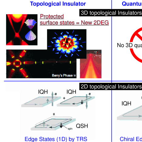
Recently, a third type of 2D topological insulator, the spin quantum Hall insulator, was theoretically predicted 14 ; 8 and then experimentally discovered 7 . This class of quantum Hall-like topological phases can exist in spin-orbit materials without external magnetic fields, and can be described as an ordinary quantum Hall state in a spin-dependent magnetic field. Their topological order gives rise to counter-propagating 1D edge states that carry opposite spin polarization, often described as a superposition of a spin up and spin down quantum Hall edge state (Figure 1). Like conventional quantum Hall systems, the 2D spin quantum Hall insulator (QSH) is realized at a buried solid interface. The first, and to date only, realization of this phase was made in (Hg,Cd)Te quantum wells using charge transport by measuring a longitudinal conductance of about at mK temperatures 7 . The quantum spin Hall state (QSH) can be thought of as two copies of integer quantum Hall states (IQH) and protected by a Z2 invariant.
It was also realized that a fundamentally new type of genuinely three-dimensional topological order might be realized in bulk crystals without need for an external magnetic field Fu:STI2 ; 11 ; 15 . Such a 3D topological insulator cannot be reduced to multiple copies of the IQH and such phases would be only the fourth type of topologically ordered phase to be discovered in nature, and the first type to fall outside the quantum Hall-like 2D topological states (IQH, FQH, QSH). Instead of having quantum-Hall type 1D edge state, these so-called 3D topological insulators would possess unconventional metallic 2D topological surface states called spin-textured helical metals, a type of 2D electron gas long thought to be impossible to realize. However, it was recognized that 3D topological insulators would NOT necessarily exhibit a topologically (Z2) quantized charge transport by themselves as carried out in a conventional transport settings of all quantum-Hall-like measurements. Therefore, their 3D topological quantum numbers (Z2), the analogues of (Chern numbers), could not be measured via the charge transport based methods even if a complete isolation of surface charge transport becomes routinely possible. Owing to the 2D nature of the two surface conduction channels that contribute together in a 3D topological insulator case, it was theoretically recognized that it would not be possible to measure the topological invariants due to the lack of a quantized transport response of the 2D surface that measures the Z2 topological invariants Fu:STI2 .
Here we review the development of spin- and angle-resolved photoemission spectroscopy (spin-ARPES) as the new approach/method to probe 3D topological order 10 ; Science , which today constitutes the experimental standard for identifying topological order in bulk solids also used by many others world-wide. We will review the procedures for i) separating intrinsic bulk bands from surface electronic structures using incident energy modulated ARPES, ii) mapping the surface electronic structure across the Kramers momenta to establish the topologically non-trivial nature of the surface states, iii) using spin-ARPES to map the spin texture of the surface states to reveal topological quantum numbers and Berry’s phases and iv) measuring the topological parent compounds to establish the microscopic origins of 3D topological order. These will be discussed in the context of Bi1-xSbx, which was the first 3D topological insulator to be experimentally discovered in nature and a textbook example of how this method is applied. The confluence of three factors, having a detailed spectroscopic procedure to measure 3D topological order, their discovery in fairly simple bulk semiconductors and being able to work at room temperatures, has led to worldwide efforts to study 3D topological physics and led to over 100 compounds being identified as 3D topological insulators to date.
II Separation of insulating bulk from metallic surface states using incident photon energy modulated ARPES
Three-dimensional topological order is predicted to occur in semiconductors with an inverted band gap, therefore 3D topological insulators are often searched for in systems where a band gap inversion is known to take place as a function of some control parameter. The experimental signature of being in the vicinity of a bulk band inversion is that the bulk band dispersion should be described by the massive Dirac equation rather than Schroedinger equation, since the system must be described by the massless Dirac equation exactly at the bulk band inversion point.
The early theoretical treatments 11 ; Murakami focused on the strongly spin-orbit coupled, band-inverted Bi1-xSbx series as a possible realization of 3D topological order for the following reason. Bismuth is a semimetal with strong spin-orbit interactions. Its band structure is believed to feature an indirect negative gap between the valence band maximum at the T point of the bulk Brillouin zone (BZ) and the conduction band minima at three equivalent L points Lenoir ; Liu (here we generally refer to these as a single point, L). The valence and conduction bands at L are derived from antisymmetric (La) and symmetric (Ls) -type orbitals, respectively, and the effective low-energy Hamiltonian at this point is described by the (3+1)-dimensional relativistic Dirac equation Wolff ; Fukuyama ; Buot . The resulting dispersion relation, , is highly linear owing to the combination of an unusually large band velocity and a small gap (such that Å-1) and has been used to explain various peculiar properties of bismuth Wolff ; Fukuyama ; Buot . Substituting bismuth with antimony is believed to change the critical energies of the band structure as follows (see Fig.2). At an Sb concentration of , the gap between La and Ls closes and a massless three-dimensional (3D) Dirac point is realized. As is further increased this gap re-opens with inverted symmetry ordering, which leads to a change in sign of at each of the three equivalent L points in the BZ. For concentrations greater than there is no overlap between the valence band at T and the conduction band at L, and the material becomes an inverted-band insulator. Once the band at T drops below the valence band at L, at , the system evolves into a direct-gap insulator whose low energy physics is dominated by the spin-orbit coupled Dirac particles at L 11 ; Lenoir .
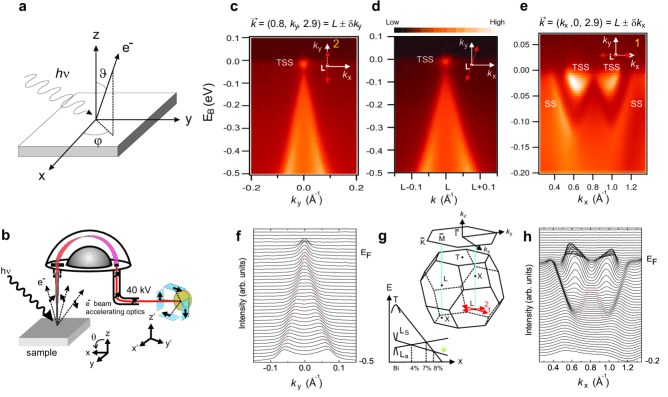
High-momentum-resolution angle-resolved photoemission spectroscopy performed with varying incident photon energy (IPEM-ARPES) allows for measurement of electronic band dispersion along various momentum space (-space) trajectories in the 3D bulk BZ. ARPES spectra taken along two orthogonal cuts through the L point of the bulk BZ of Bi0.9Sb0.1 are shown in Figs 1a and c. A -shaped dispersion whose tip lies less than 50 meV below the Fermi energy () can be seen along both directions. Additional features originating from surface states that do not disperse with incident photon energy are also seen. Owing to the finite intensity between the bulk and surface states, the exact binding energy () where the tip of the -shaped band dispersion lies is unresolved. The linearity of the bulk -shaped bands is observed by locating the peak positions at higher in the momentum distribution curves (MDCs), and the energy at which these peaks merge is obtained by extrapolating linear fits to the MDCs. Therefore 50 meV represents a lower bound on the energy gap between La and Ls. The magnitude of the extracted band velocities along the and directions are ms-1 and ms-1, respectively, which are similar to the tight binding values ms-1 and ms-1 calculated for the La band of bismuth Liu . Our data are consistent with the extremely small effective mass of (where is the electron mass) observed in magneto-reflection measurements on samples with Hebel . The Dirac point in graphene, co-incidentally, has a band velocity ( ms-1) Zhang comparable to what we observe for Bi0.9Sb0.1, but its spin-orbit coupling is several orders of magnitude weaker, and the only known method of inducing a gap in the Dirac spectrum of graphene is by coupling to an external chemical substrate Zhou . The Bi1-xSbx series thus provides a rare opportunity to study relativistic Dirac Hamiltonian physics in a 3D condensed matter system where the intrinsic (rest) mass gap can be easily tuned.
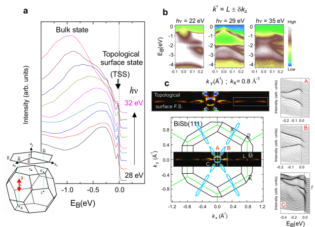
Studying the band dispersion perpendicular to the sample surface provides a way to differentiate bulk states from surface states in a 3D material. To visualize the near- dispersion along the 3D L-X cut (X is a point that is displaced from L by a distance of 3, where is the lattice constant), in Fig.2a we plot energy distribution curves (EDCs), taken such that electrons at have fixed in-plane momentum = (Lx, Ly) = (0.8 Å-1, 0.0 Å-1), as a function of photon energy (). There are three prominent features in the EDCs: a non-dispersing, independent, peak centered just below at about 0.02 eV; a broad non-dispersing hump centered near 0.3 eV; and a strongly dispersing hump that coincides with the latter near = 29 eV. To understand which bands these features originate from, we show ARPES intensity maps along an in-plane cut (parallel to the direction) taken using values of 22 eV, 29 eV and 35 eV, which correspond to approximate values of L 0.3 Å-1, Lz, and Lz + 0.3 Å-1 respectively (Fig.2b). At = 29 eV, the low energy ARPES spectral weight reveals a clear -shaped band close to . As the photon energy is either increased or decreased from 29 eV, this intensity shifts to higher binding energies as the spectral weight evolves from the -shaped into a -shaped band. Therefore the dispersive peak in Fig.2a comes from the bulk valence band, and for = 29 eV the high symmetry point L = (0.8, 0, 2.9) appears in the third bulk BZ. In the maps of Fig.2b with respective values of 22 eV and 35 eV, overall weak features near that vary in intensity remain even as the bulk valence band moves far below . The survival of these weak features over a large photon energy range (17 to 55 eV) supports their surface origin. The non-dispersing feature centered near eV in Fig.2a comes from the higher binding energy (valence band) part of the full spectrum of surface states, and the weak non-dispersing peak at eV reflects the low energy part of the surface states that cross away from the point and forms the surface Fermi surface (Fig.2c).
III Winding number count: Counting of surface Fermi surfaces enclosing Kramers points to identify topologically non-trivial surface spin-textured states
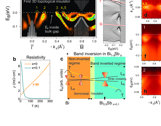
Having established the existence of an energy gap in the bulk state of Bi0.9Sb0.1 (Figs 1 and 2) and observed linearly dispersive bulk bands uniquely consistent with strong spin-orbit coupling model calculations Wolff ; Fukuyama ; Buot ; Liu (see SM for full comparison with theoretical calculation), we now discuss the topological character of its surface states, which are found to be gapless (Fig.2c). In general, the states at the surface of spin-orbit coupled compounds are allowed to be spin split owing to the loss of space inversion symmetry . However, as required by Kramers’ theorem, this splitting must go to zero at the four time reversal invariant momenta (TRIM) in the 2D surface BZ. As discussed in 11 ; Fu:STI2 , along a path connecting two TRIM in the same BZ, the Fermi energy inside the bulk gap will intersect these singly degenerate surface states either an even or odd number of times. When there are an even number of surface state crossings, the surface states are topologically trivial because weak disorder (as may arise through alloying) or correlations can remove pairs of such crossings by pushing the surface bands entirely above or below . When there are an odd number of crossings, however, at least one surface state must remain gapless, which makes it non-trivial 11 ; Murakami ; Fu:STI2 . The existence of such topologically non-trivial surface states can be theoretically predicted on the basis of the bulk band structure only, using the invariant that is related to the quantum Hall Chern number 14 . Materials with band structures with are ordinary Bloch band insulators that are topologically equivalent to the filled shell atomic insulator, and are predicted to exhibit an even number (including zero) of surface state crossings. Materials with bulk band structures with on the other hand, which are expected to exist in rare systems with strong spin-orbit coupling acting as an internal quantizing magnetic field on the electron system Haldane(P-anomaly) , and inverted bands at an odd number of high symmetry points in their bulk 3D BZs, are predicted to exhibit an odd number of surface state crossings, precluding their adiabatic continuation to the atomic insulator 11 ; Murakami ; Fu:STI2 ; 15 ; 8 ; 7 . Such “topological quantum Hall metals” Fu:STI2 ; 15 cannot be realized in a purely 2D electron gas system such as the one realized at the interface of GaAs/GaAlAs systems.
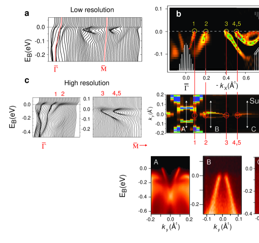
In our experimental case, namely the (111) surface of Bi0.9Sb0.1, the four TRIM are located at and three points that are rotated by relative to one another. Owing to the three-fold crystal symmetry (A7 bulk structure) and the observed mirror symmetry of the surface Fermi surface across (Fig.2), these three points are equivalent (and we henceforth refer to them as a single point, ). The mirror symmetry is also expected from time reversal invariance exhibited by the system. The complete details of the surface state dispersion observed in our experiments along a path connecting and are shown in Fig.3a; finding this information is made possible by our experimental separation of surface states from bulk states. As for bismuth (Bi), two surface bands emerge from the bulk band continuum near to form a central electron pocket and an adjacent hole lobe Ast:Bi1 ; Hochst ; Hofmann . It has been established that these two bands result from the spin-splitting of a surface state and are thus singly degenerate Hirahara ; Hofmann . On the other hand, the surface band that crosses at Å-1, and forms the narrow electron pocket around , is clearly doubly degenerate, as far as we can determine within our experimental resolution. This is indicated by its splitting below between Å-1 and , as well as the fact that this splitting goes to zero at in accordance with Kramers theorem. In semimetallic single crystal bismuth, only a single surface band is observed to form the electron pocket around Hengsberger ; Ast:Bi2 . Moreover, this surface state overlaps, hence becomes degenerate with, the bulk conduction band at L (L projects to the surface point) owing to the semimetallic character of Bi (Fig.3b). In Bi0.9Sb0.1 on the other hand, the states near fall completely inside the bulk energy gap preserving their purely surface character at (Fig.3a). The surface Kramers doublet point can thus be defined in the bulk insulator (unlike in Bi Hirahara ; Ast:Bi1 ; Hochst ; Hofmann ; Hengsberger ; Ast:Bi2 ) and is experimentally located in Bi0.9Sb0.1 samples to lie approximately 15 5 meV below at (Fig.3a). For the precise location of this Kramers point, it is important to demonstrate that our alignment is strictly along the line. To do so, we contrast high resolution ARPES measurements taken along the line with those that are slightly offset from it (Fig.3e). Figs 3f-i show that with offset from the Kramers point at by less than 0.02 Å-1, the degeneracy is lifted and only one band crosses to form part of the bow-shaped electron distribution (Fig.3d). Our finding of five surface state crossings (an odd rather than an even number) between and (Fig.3a), confirmed by our observation of the Kramers degenerate point at the TRIM, indicates that these gapless surface states are topologically non-trivial. This corroborates our bulk electronic structure result that Bi0.9Sb0.1 is in the insulating band-inverted () regime (Fig.3c), which contains an odd number of bulk (gapped) Dirac points, and is topologically analogous to an integer quantum spin Hall insulator.
Our experimental results taken collectively strongly suggest that Bi0.9Sb0.1 is quite distinct from graphene Zhang ; Novoselov and represents a novel state of quantum matter: a strongly spin-orbit coupled insulator with an odd number of Dirac points with a negative topological Hall phase, which realizes the “parity anomaly without Fermion doubling”. Our work further demonstrates a general methodology for possible future investigations of novel topological orders in exotic quantum matter.
IV Spin-resolving the surface states to identify the non-trivial topological phase and establish a 2D helical metal protected from backscattering
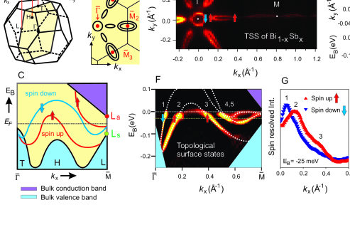
Strong topological materials are distinguished from ordinary materials such as gold by a topological quantum number, = 1 or 0 respectively 14 ; 15 . For Bi1-xSbx, theory has shown that is determined solely by the character of the bulk electronic wave functions at the point in the three-dimensional (3D) Brillouin zone (BZ). When the lowest energy conduction band state is composed of an antisymmetric combination of atomic -type orbitals () and the highest energy valence band state is composed of a symmetric combination (), then = 1, and vice versa for = 0 11 . Although the bonding nature (parity) of the states at is not revealed in a measurement of the bulk band structure, the value of can be determined from the spin-textures of the surface bands that form when the bulk is terminated. In particular, a = 1 topology requires the terminated surface to have a Fermi surface (FS) that supports a non-zero Berry’s phase (odd as opposed to even multiple of ), which is not realizable in an ordinary spin-orbit material.
In a general inversion symmetric spin-orbit insulator, the bulk states are spin degenerate because of a combination of space inversion symmetry and time reversal symmetry . Because space inversion symmetry is broken at the terminated surface, the spin degeneracy of surface bands can be lifted by the spin-orbit interaction [19-21]. However, according to Kramers theorem [16], they must remain spin degenerate at four special time reversal invariant momenta ( = , M̄) in the surface BZ [11], which for the (111) surface of Bi1-xSbx are located at and three equivalent M̄ points [see Fig.5(A)].
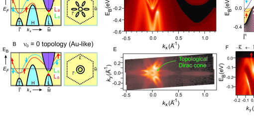
Depending on whether equals 0 or 1, the Fermi surface pockets formed by the surface bands will enclose the four an even or odd number of times respectively. If a Fermi surface pocket does not enclose (= , M̄), it is irrelevant for the topology 11 ; 20 . Because the wave function of a single electron spin acquires a geometric phase factor of 16 ; 17 as it evolves by 360∘ in momentum space along a Fermi contour enclosing a , an odd number of Fermi pockets enclosing in total implies a geometrical (Berry’s) phase 11 . In order to realize a Berry’s phase the surface bands must be spin-polarized and exhibit a partner switching 11 dispersion behavior between a pair of . This means that any pair of spin-polarized surface bands that are degenerate at must not re-connect at M̄, or must separately connect to the bulk valence and conduction band in between and M̄. The partner switching behavior is realized in Fig. 5(C) because the spin down band connects to and is degenerate with different spin up bands at and M̄. The partner switching behavior is realized in Fig. 7(A) because the spin up and spin down bands emerging from separately merge into the bulk valence and conduction bands respectively between and M̄.
We first investigate the spin properties of the topological insulator phase Science . Spin-integrated ARPES 19 intensity maps of the (111) surface states of insulating Bi1-xSbx taken at the Fermi level () [Figs 5(D)&(E)] show that a hexagonal FS encloses , while dumbbell shaped FS pockets that are much weaker in intensity enclose M̄. By examining the surface band dispersion below the Fermi level [Fig.5(F)] it is clear that the central hexagonal FS is formed by a single band (Fermi crossing 1) whereas the dumbbell shaped FSs are formed by the merger of two bands (Fermi crossings 4 and 5) 10 .
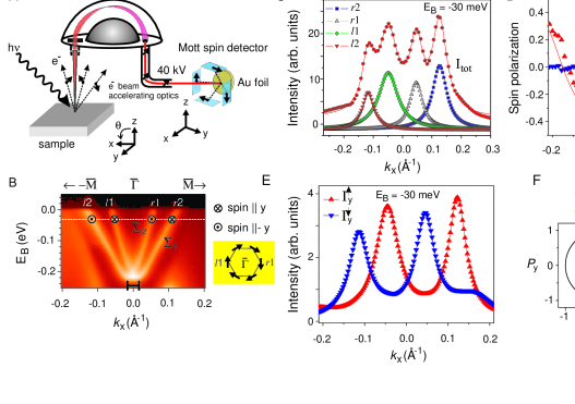
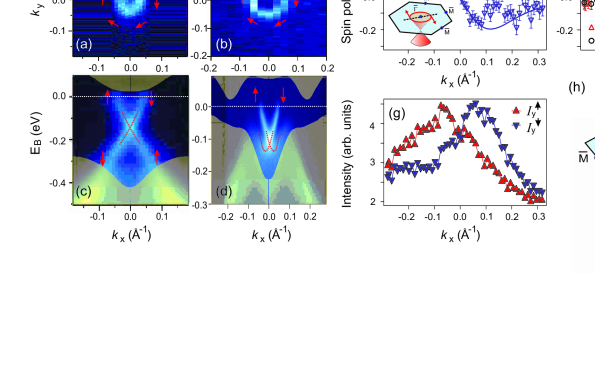
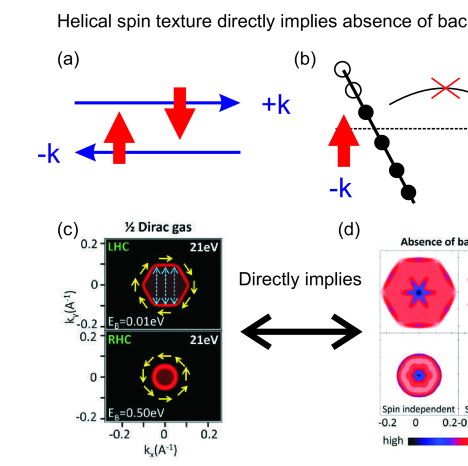
This band dispersion resembles the partner switching dispersion behavior characteristic of topological insulators. To check this scenario and determine the topological index , we have carried out spin-resolved photoemission spectroscopy. Fig.5(G) shows a spin-resolved momentum distribution curve taken along the -M̄ direction at a binding energy = 25 meV [Fig.5(G)]. The data reveal a clear difference between the spin-up and spin-down intensities of bands 1, 2 and 3, and show that bands 1 and 2 have opposite spin whereas bands 2 and 3 have the same spin (detailed analysis discussed later in text). The former observation confirms that bands 1 and 2 form a spin-orbit split pair, and the latter observation suggests that bands 2 and 3 (as opposed to bands 1 and 3) are connected above the Fermi level and form one band. This is further confirmed by directly imaging the bands through raising the chemical potential via doping (SM). Irrelevance of bands 2 and 3 to the topology is consistent with the fact that the Fermi surface pocket they form does not enclose any . Because of a dramatic intrinsic weakening of signal intensity near crossings 4 and 5, and the small energy and momentum splitting of bands 4 and 5 lying at the resolution limit of modern spin-resolved ARPES spectrometers, no conclusive spin information about these two bands can be drawn from the methods employed in obtaining the data sets in Figs 5(G)&(H). However, whether bands 4 and 5 are both singly or doubly degenerate does not change the fact that an odd number of spin-polarized FSs enclose the , which provides evidence that Bi1-xSbx has = 1 and that its surface supports a non-trivial Berry’s phase. This directly implies an absence of backscattering in electronic transport along the surface (Fig.11).
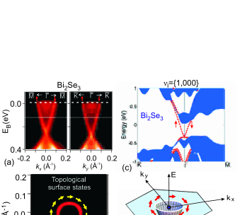
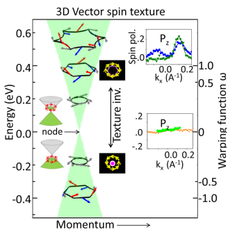
Shortly after the discovery of Bi1-xSbx, physicists sought to find a simpler version of a 3D topological insulator consisting of a single surface state instead of five. This is because the surface structure of Bi1-xSbx was rather complicated and the band gap was rather small. This motivated a search for topological insulators with a larger band gap and simpler surface spectrum. A second generation of 3D topological insulator materials, especially Bi2Se3, offers the potential for topologically protected behavior in ordinary crystals at room temperature and zero magnetic field. Starting in 2008, work by the Princeton group used spin-ARPES and first-principles calculations to study the surface band structure of Bi2Se3 and observe the characteristic signature of a topological insulator in the form of a single Dirac cone that is spin-polarized (Figs 6 and 10) such that it also carries a non-trivial Berry’s phase Xia ; Nature_2009 . Concurrent theoretical work by Zhang_nphys used electronic structure methods to show that Bi2Se3 is just one of several new large band-gap topological insulators. These other materials were soon after also identified using this ARPES technique we describe Chen ; Hsieh_PRL .
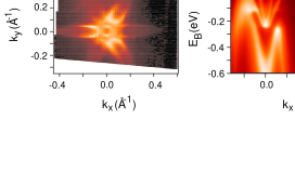
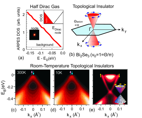
The Bi2Se3 surface state is found from spin-ARPES and theory to be a nearly idealized single Dirac cone as seen from the experimental data in Figs.6 and 14. An added advantage is that Bi2Se3 is stoichiometric (i.e., a pure compound rather than an alloy such as Bi1-xSbx) and hence can be prepared, in principle, at higher purity. While the topological insulator phase is predicted to be quite robust to disorder, many experimental probes of the phase, including ARPES of the surface band structure, are clearer in high-purity samples. Finally and perhaps most important for applications, Bi2Se3 has a large band gap of around 0.3 eV (3600 K). This indicates that in its high-purity form Bi2Se3 can exhibit topological insulator behavior at room temperature and greatly increases the potential for applications, which we discuss in greater depth later in the review.
V Identifying the origin of 3D topological order via a bulk band gap inversion transition
We investigated the quantum origin of topological order in this class of materials. It has been theoretically speculated that the novel topological order originates from the parities of the electrons in pure Sb and not Bi 11 ; Lenoir . It was also noted 20 that the origin of the topological effects can only be tested by measuring the spin-texture of the Sb surface, which has not been measured. Based on quantum oscillation and magneto-optical studies, the bulk band structure of Sb is known to evolve from that of insulating Bi1-xSbx through the hole-like band at H rising above and the electron-like band at sinking below Lenoir . The relative energy ordering of the and states in Sb again determines whether the surface state pair emerging from switches partners [Fig.7(A)] or not [Fig.7(B)] between and M̄, and in turn determines whether they support a non-zero Berry’s phase.
In a conventional spin-orbit metal such as gold, a free-electron like surface state is split into two parabolic spin-polarized sub-bands that are shifted in -space relative to each other 18 . Two concentric spin-polarized Fermi surfaces are created, one having an opposite sense of in-plane spin rotation from the other, that enclose . Such a Fermi surface arrangement, like the schematic shown in figure 7(B), does not support a non-zero Berry’s phase because the are enclosed an even number of times (2 for most known materials).
However, for Sb, this is not the case. Figure 7(C) shows a spin-integrated ARPES intensity map of Sb(111) from to M̄. By performing a systematic incident photon energy dependence study of such spectra, previously unavailable with He lamp sources 24 , it is possible to identify two V-shaped surface states (SS) centered at , a bulk state located near = 0.25 Å-1 and resonance states centered about = 0.25 Å-1 and M̄ that are hybrid states formed by surface and bulk states 19 (SM). An examination of the ARPES intensity map of the Sb(111) surface and resonance states at [Fig.7(E)] reveals that the central surface FS enclosing is formed by the inner V-shaped SS only. The outer V-shaped SS on the other hand forms part of a tear-drop shaped FS that does not enclose , unlike the case in gold. This tear-drop shaped FS is formed partly by the outer V-shaped SS and partly by the hole-like resonance state. The electron-like resonance state FS enclosing M̄ does not affect the determination of because it must be doubly spin degenerate (SM). Such a FS geometry [Fig.7(G)] suggests that the V-shaped SS pair may undergo a partner switching behavior expected in Fig.7(A). This behavior is most clearly seen in a cut taken along the -K̄ direction since the top of the bulk valence band is well below [Fig.7(F)] showing only the inner V-shaped SS crossing while the outer V-shaped SS bends back towards the bulk valence band near = 0.1 Å-1 before reaching . The additional support for this band dispersion behavior comes from tight binding surface calculations on Sb [Fig.7(D)], which closely match with experimental data below . Our observation of a single surface band forming a FS enclosing suggests that pure Sb is likely described by = 1, and that its surface may support a Berry’s phase.
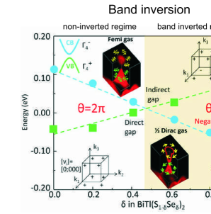
Confirmation of a surface Berry’s phase rests critically on a measurement of the relative spin orientations (up or down) of the SS bands near so that the partner switching is indeed realized, which cannot be done without spin resolution. Spin resolution was achieved using a Mott polarimeter that measures two orthogonal spin components of a photoemitted electron 27 ; 28 . These two components are along the and directions of the Mott coordinate frame, which lie predominantly in and out of the sample (111) plane respectively. Each of these two directions represents a normal to a scattering plane defined by the photoelectron incidence direction on a gold foil and two electron detectors mounted on either side (left and right) [Fig.9(A)]. Strong spin-orbit coupling of atomic gold is known to create an asymmetry in the scattering of a photoelectron off the gold foil that depends on its spin component normal to the scattering plane 28 . This leads to an asymmetry between the left intensity () and right intensity () given by , which is related to the spin polarization through the Sherman function = 0.085 27 ; 28 . Spin-resolved momentum distribution curve data sets of the SS bands along the M̄--M̄ cut at = 30 meV [Fig.9(B)] are shown for maximal intensity. Figure 9(D) displays both and polarization components along this cut, showing clear evidence that the bands are spin polarized, with spins pointing largely in the (111) plane. In order to estimate the full 3D spin polarization vectors from a two component measurement (which is not required to prove the partner switching or the Berry’s phase), we fit a model polarization curve to our data following the recent demonstration in Ref-26 , which takes the polarization directions associated with each momentum distribution curve peak [Fig.9(C)] as input parameters, with the constraint that each polarization vector has length one (in angular momentum units of /2). Our fitted polarization vectors are displayed in the sample () coordinate frame [Fig.9(F)], from which we derive the spin-resolved momentum distribution curves for the spin components parallel () and anti-parallel () to the direction (SM) as shown in figure 9(E). There is a clear difference in and at each of the four momentum distribution curve peaks indicating that the surface state bands are spin polarized [Fig.9(E)], which is possible to conclude even without a full 3D fitting. Each of the pairs and have opposite spin, consistent with the behavior of a spin split pair, and the spin polarization of these bands are reversed on either side of in accordance with the system being time reversal symmetric [Fig.9(F)]. The measured spin texture of the Sb(111) surface states (Fig.9), together with the connectivity of the surface bands (Fig.7), uniquely determines its belonging to the = 1 class. Therefore the surface of Sb carries a non-zero () Berry’s phase via the inner V-shaped band and pure Sb can be regarded as the parent metal of the Bi1-xSbx topological insulator class, in other words, the topological order originates from the Sb wave functions. A recent work Xu has demonstrated a topological quantum phase transition as a function of chemical composition from a non-inverted to an inverted semiconductor as a clear example of the origin of topological order (Fig.8).
Our spin polarized measurement methods (Fig.5 and 9) uncover a new type of topological quantum number which provides information about the chirality properties. Topological band theory suggests that the bulk electronic states in the mirror ( = 0) plane can be classified in terms of a number (=1) that describes the handedness (either left or right handed) or chirality of the surface spins which can be directly measured or seen in spin-resolved experiments 20 . We now determine the value of from our data. From figure 5, it is seen that a single (one) surface band, which switches partners at M̄, connects the bulk valence and conduction bands, so = 1 (SM). The sign of is related to the direction of the spin polarization of this band 20 , which is constrained by mirror symmetry to point along . Since the central electron-like FS enclosing intersects six mirror invariant points [see Fig.9(B)], the sign of distinguishes two distinct types of handedness for this spin polarized FS. Figures 5(F) and 9 show that for both Bi1-xSbx and Sb, the surface band that forms this electron pocket has along the direction, suggesting a left-handed rotation sense for the spins around this central FS thus = 1. Therefore, both insulating Bi1-xSbx and pure Sb possess equivalent chirality properties a definite spin rotation sense (left-handed chirality, see Fig.9(B)) and a topological Berry’s phase. Recently a chirality transition across the surface Dirac point of a 3D topological insulator has also been observed using spin-ARPES Xu (Fig.12).
These spin-resolved experimental measurements reveal an intimate and straightforward connection between the topological numbers (, ) and the physical observables. The determines whether the surface electrons support a non-trivial Berry’s phase, and if they do, the determines the spin handedness of the Fermi surface that manifests this Berry’s phase. The 2D Berry’s phase is a critical signature of topological order and is not realizable in isolated 2D electron systems, nor on the surfaces of conventional spin-orbit or exchange coupled magnetic materials. A non-zero Berry’s phase is known, theoretically, to protect an electron system against the almost universal weak-localization behavior in their low temperature transport 11 ; 13 and is expected to form the key element for fault-tolerant computation schemes 13 ; 29 , because the Berry’s phase is a geometrical agent or mechanism for protection against quantum decoherence 30 . Its remarkable realization on the Bi1-xSbx surface represents an unprecedented example of a 2D Berry’s phase, and opens the possibility for building realistic prototype systems to test quantum computing modules. In general, our results demonstrate that spin-ARPES is a powerful probe of 3D topological order, which opens up a new search front for topological materials for novel spin-devices and fault-tolerant quantum computing.
VI Topological protection and tunability of the surface states of a 3D topological insulator
The predicted topological protection of the surface states of Sb implies that their metallicity cannot be destroyed by weak time reversal symmetric perturbations. In order to test the robustness of the measured gapless surface states of Sb, we introduce such a perturbation by randomly substituting Bi into the Sb crystal matrix. Another motivation for performing such an experiment is that the formalism developed by Fu and Kane 11 to calculate the topological invariants relies on inversion symmetry being present in the bulk crystal, which they assumed to hold true even in the random alloy Bi1-xSbx. However, this formalism is simply a device for simplifying the calculation and the non-trivial topological class of Bi1-xSbx is predicted to hold true even in the absence of inversion symmetry in the bulk crystal 11 . Therefore introducing light Bi substitutional disorder into the Sb matrix is also a method to examine the effects of alloying disorder and possible breakdown of bulk inversion symmetry on the surface states of Sb(111). We have performed spin-integrated ARPES measurements on single crystals of the random alloy Sb0.9Bi0.1. Figure 13 shows that both the surface band dispersion along -M̄ as well as the surface state Fermi surface retain the same form as that observed in Sb(111), and therefore the ‘topological metal’ surface state of Sb(111) fully survives the alloy disorder. Since Bi alloying is seen to only affect the band structure of Sb weakly, it is reasonable to assume that the topological order is preserved between Sb and Bi0.91Sb0.09 as we observed.
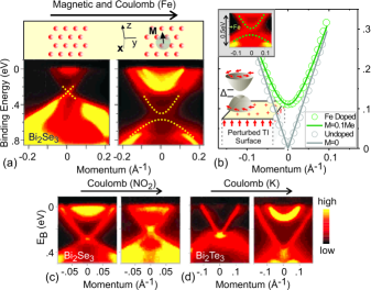
In a simpler fashion compared to Bi1-xSbx, the topological insulator behavior in Bi2Se3 is associated with a single band inversion at the surface Brillouin zone center. Owing to its larger bandgap compared with Bi1-xSbx, ARPES has shown that its topological properties are preserved at room temperature Nature_2009 . Two defining properties of topological insulators spin-momentum locking of surface states and Berry phase can be clearly demonstrated in the Bi2Se3 series. The surface states are expected to be protected by time-reversal symmetry symmetry, which implies that the surface Dirac node should be robust in the presence of nonmagnetic disorder but open a gap in the presence of time-reversal symmetry breaking perturbations. Magnetic impurities such as Fe or Mn on the surface of Bi2Se3 open a gap at the Dirac point [Figs. 15(a) and 15(b)] Hor ; Wray . The magnitude of the gap is likely set by the interaction of Fe ions with the Se surface and the time-reversal symmetry breaking disorder potential introduced on the surface. Nonmagnetic disorder created via molecular absorbent NO2 or alkali atom adsorption (K or Na) on the surface leaves the Dirac node intact [Figs. 15(c) and 15(d)] in both Bi2Se3 and Bi2Te3 Nature_2009 ; Xia_arxiv . These results are consistent with the fact that the topological surface states are protected by time-reversal symmetry.
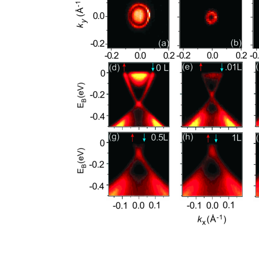
Many of the interesting theoretical proposals that utilize topological insulator surfaces require the chemical potential to lie at or near the surface Dirac point. This is similar to the case in graphene, where the chemistry of carbon atoms naturally locates the Fermi level at the Dirac point. This makes its density of carriers highly tunable by an applied electrical field and enables applications of graphene to both basic science and microelectronics. The surface Fermi level of a topological insulator depends on the detailed electrostatics of the surface and is not necessarily at the Dirac point. Moreover, for naturally grown Bi2Se3 the bulk Fermi energy is not even in the gap. The observed n-type behavior is believed to be caused Se vacancies. By appropriate chemical modifications, however, the Fermi energy of both the bulk and the surface can be controlled. This allowed Nature_2009 to reach the sweet spot in which the surface Fermi energy is tuned to the Dirac point (Fig.16). This was achieved by doping bulk with a small concentration of Ca, which compensates the Se vacancies, to place the Fermi level within the bulk band gap. The surface was the hole doped by exposing the surface to NO2 gas to place the Fermi level at the Dirac point. These results collectively show how ARPES can be used to study the topological protection and tunability properties of the 2D surface of a 3D topological insulator.
VII Future directions: Identifying Majorana Platforms and Topological Superconductors
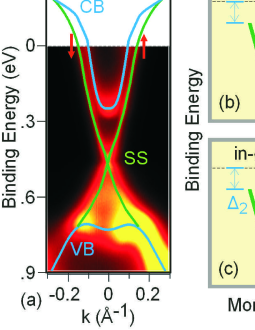
Recent measurements Wray show that surface instabilities cause the spin-helical topological insulator band structure of Bi2Se3 to remain well defined and non- degenerate with bulk electronic states at the Fermi level of optimally doped superconducting Cu0.12Bi2Se3, and that this is also likely to be the case for superconduct- ing variants of p-type Bi2Te3. These surface states pro- vide a highly unusual physical setting in which super- conductivity cannot take a conventional form, and is expected to realize one of two novel states that have not been identified elsewhere in nature. If superconducting pairing has even parity, as is nearly universal among the known superconducting materials, the surface electrons will achieve a 2D non-Abelian superconductor state with non-commutative Majorana fermion vortices that can potentially be manipulated to store quantum information. Surface vortices will be found at the end of bulk vortex lines as drawn in Fig.17. If superconducting pairing is odd, the resulting state is a novel state of matter known as a “topological superconductor” with Bogoliubov surface quasi-particles present below the superconducting critical temperature of 3.8 K. As drawn in Fig.17(c), these low temperature surface states would be gapless, likely making it impossible to adiabatically manipulate surface vortices for quantum computation. The unique physics and applications of the topological superconductor state are distinct from any known material system, and will be an exciting vista for theoretical and experimental exploration if they are achieved for the first time in CuxBi2Se3.
Acknowledgement The authors acknowledge collaborations with A. Bansil, R. J. Cava, J.H. Dil, A. V. Fedorov, Liang Fu, Y. S. Hor, S. Jia, H. Lin, F. Meier, N. P. Ong, J. Osterwalder, L. Patthey, D. Qian and A. Yazdani for collaborations and U.S. DOE Grants No. DE-FG-02-05ER46200, No. AC03-76SF00098, and No. DE-FG02-07ER46352. M.Z.H. acknowledges visiting-scientist support from Lawrence Berkeley National Laboratory and additional support from the A.P. Sloan Foundation.
VIII Supplementary materials
VIII.1 Growth method for high-quality single crystals
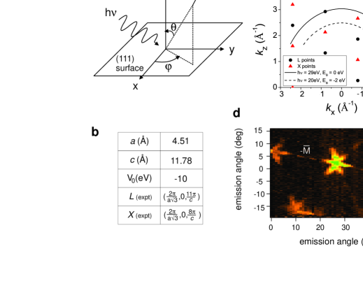
The undoped and doped Bi1-xSbx single-crystal samples () used for ARPES experiments were each cleaved from a boule grown from a stoichiometric mixture of high-purity elements. The boule was cooled from 650 ∘C to 270 ∘C over a period of five days and was annealed for seven days at 270 ∘C. The samples naturally cleaved along the (111) plane, which resulted in shiny flat silver surfaces. X-ray diffraction measurements were used to check that the samples were single phase, and confirmed that the Bi0.9Sb0.1 single crystals presented in this paper have a rhombohedral A7 crystal structure (point group ), with room-temperature (T=300K) lattice parameters = 4.51 Å and = 11.78 Å indexed using a rhombohedral unit cell. The X-ray diffraction patterns of the cleaved crystals exhibit only the (333), (666), and (999) peaks, showing that the cleaved surface is oriented along the trigonal (111) axis. Room-temperature data were recorded on a Bruker D8 diffractometer using Cu K radiation ( = 1.54 Å) and a diffracted-beam monochromator. The in-plane crystal orientation was determined by Laue X-ray diffraction. During the angle-resolved photoemission spectroscopy (ARPES) measurements a fine alignment was achieved by carefully studying the band dispersions and Fermi surface symmetry as an internal check for crystal orientation.
VIII.2 Resistivity characterization
Temperature-dependent resistivity measurements were carried out on single-crystal samples in a Quantum Design PPMS-9 instrument, using a standard four-probe technique on approximately 4 1 1-mm3, rectangular samples with the current in the basal plane, which was perpendicular to the trigonal axis. The four contacts were made by using room-temperature silver paste. The data for samples with concentrations ranging from = 0 to = 0.17 showed a systematic change from semimetallic to insulating-like behaviour with increasing , in agreement with previously published works Fukuyama , which was used as a further check of the antimony concentrations. Conventional magnetic and transport measurements 7 ; Lenoir ; Kopelovic such as these cannot separately measure the contributions of the surface and bulk states to the total signal. ARPES, on the other hand, is a momentum-selective technique 19 , which allows for a separation of 2D (surface) from 3D (bulk) dispersive energy bands. This capability is especially important for Bi1-xSbx because the Dirac point lies at a single point in the 3D Brillouin zone, unlike for 2D graphene, where the Dirac points can be studied at any arbitrary perpendicular momentum along a line Novoselov ; Bostwick .
VIII.3 ARPES
Spin-integrated angle-resolved photoemission spectroscopy (ARPES) measurements were performed with 14 to 30 eV photons on beam line 5-4 at the Stanford Synchrotron Radiation Laboratory, and with 28 to 32 eV photons on beam line 12 at the Advanced Light Source, both endstations being equipped with a Scienta hemispherical electron analyzer (see VG Scienta manufacturer website for instrument specifications). Spin-resolved ARPES measurements were performed at the SIS beam line at the Swiss Light Source using the COPHEE spectrometer (31 p.15) with a single 40 kV classical Mott detector and photon energies of 20 and 22 eV. The typical energy and momentum resolution was 15 meV and 1.5% of the surface Brillouin zone (BZ) respectively at beam line 5-4, 9 meV and 1% of the surface BZ respectively at beam line 12, and 80 meV and 3% of the surface BZ respectively at SIS using a pass energy of 3 eV. Cleaving these samples in situ between 10 K and 55 K at chamber pressures less than 5 torr resulted in shiny flat surfaces, characterized in situ by low energy electron diffraction (LEED) to be clean and well ordered with the same symmetry as the bulk. This is consistent with photoelectron diffraction measurements that show no substantial structural relaxation of the Sb(111) surface 32 .
VIII.4 Systematic methods for separating bulk from surface electronic states
ARPES is a photon-in, electron-out technique 19 . Photoelectrons ejected from a sample by a monochromatic beam of radiation are collected by a detector capable of measuring its kinetic energy . By varying the detector angles, and , relative to the sample surface normal, the momentum of the photoelectrons, K, can also be determined (as illustrated in S1). By employing the commonly used free-electron final state approximation, we can fully convert from the measured kinetic energy and momentum values of the photoelectron to the binding energy, , and Bloch momentum values k of its initial state inside the crystal, via
where we have set = 0, is the work function, is the electron mass and is an experimentally determined parameter, which is approximately 10 eV for bismuth Jezequel ; Ast:Bi3D . Features in the ARPES spectra originating from bulk initial states (dispersive along the -direction) were distinguished from those originating from surface initial states (non-dispersive along the -direction) by studying their dependence on incident photon energy, , and converting this to dependence on via the displayed equations. ARPES data were collected at beamlines 12.0.1 and 10.0.1 of the Advanced Light Source at the Lawrence Berkeley National Laboratory, as well as at the PGM beamline of the Synchrotron Radiation Center in Wisconsin, with incident photon energies ranging from 17 eV to 55 eV, energy resolutions ranging from 9 meV to 40 meV and momentum resolution better than 1.5% of the surface Brillouin zone, using Scienta electron analysers. The combination of high spatial resolution and high crystalline quality enabled us to probe only the highly ordered and cleanest regions of our samples. Single-crystal Bi1-xSbx samples were cleaved in situ at a temperature of 15 K and chamber pressures less than 8 10-11 torr, and high surface quality was checked throughout the measurement process by monitoring the EDC linewidths of the surface state. To measure the near- dispersion of an electronic band along a direction normal to the sample surface, such as the direction from to shown in Fig. 3a, EDCs were taken at several incident photon energies. The kinetic energy of the photoelectron at is different for each value of , so the angle was first adjusted and then held fixed for each so as to keep constant at = 0.8 Å-1 for electrons emitted near . To ensure that the in-plane momentum remained constant at M̄ (the - line projects onto M̄) for each EDC, a complete near- intensity map was generated for each photon energy to precisely locate the M̄-point (see Fig.S1d). We note that because the bulk crystal has only three-fold rotational symmetry about the -axis, the reciprocal lattice does not have mirror symmetry about the = 0 plane. Therefore, scans taken at + and - for the same photon energy probe different points in the bulk 3D Brillouin zone; this is responsible for the absence of the bulk -shaped band in Fig. 4f.
VIII.5 Confirming the bulk nature of electronic bands by comparison with theoretical calculations
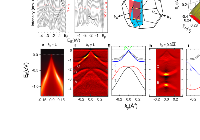
In an ARPES experiment (Fig.S1a), three dimensional (3D) dispersive bulk electronic states can be identified as those that disperse with incident photon energy, whereas surface states do not. As an additional check that we have indeed correctly identified the bulk bands of Bi0.9Sb0.1 in Figs 2 and 3, we also measured the dispersion of the deeper lying bands well below the Fermi level () and compared them to tight binding theoretical calculations of the bulk bands of pure bismuth following the model of Liu and Allen (1995) Liu . A tight-binding approach is known to be valid since Bi0.9Sb0.1 is not a strongly correlated electron system. As Bi0.9Sb0.1 is a random alloy (Sb does not form a superlattice Lenoir ) with a relatively small Sb concentration (0.2 Sb atoms per rhombohedral unit cell), the deeper lying band structure of Bi0.9Sb0.1 is expected to follow that of pure Bi because the deeper lying (localized wave function) bands of Bi0.9Sb0.1 are not greatly affected by the substitutional disorder, and no additional back folded bands are expected to arise. Since these deeper lying bands are predicted to change dramatically with , they help us to finely determine the experimentally probed values. Fig.S2f shows the ARPES second derivative image (SDI) of a cut parallel to K̄M̄K̄ that passes through the point of the 3D Brillouin zone (BZ), and Fig.S2h shows a parallel cut that passes through the 0.3 point (Fig.S2c). The locations of these two cuts in the 3D bulk BZ were calculated from the ARPES kinematic relations, from which we can construct the constant energy contours shown in Fig. S1c. By adjusting such that the in-plane momentum is fixed at approximately 0.8 Å-1 (the surface M̄ point), at a photon energy =29 eV, electrons at the Fermi energy (=0 eV) have a that corresponds to the point in the 3rd bulk BZ. By adjusting such that the in-plane momentum is fixed at approximately -0.8 Å-1, at a photon energy = 20 eV, electrons at a binding energy of -2 eV have a near 0.3 .
There is a clear dependence of the dispersion of measured bands A, B and C, pointing to their bulk nature. The bulk origin of bands A, B and C is confirmed by their good agreement with tight binding calculations (bands 3, 4 and 5 in Figs S2g and i), which include a strong spin-orbit coupling constant of 1.5 eV derived from bismuth Liu . Band 3 drops below -5 eV at the 0.3 point. The slight differences between the experimentally measured band energies and the calculated band energies at = 0 Å-1 shown in Fig.S2f-i are due to the fact that the ARPES data were collected in a single shot, taken in constant mode. This means that electrons detected at different binding energies will have slightly different values of , whereas the presented tight binding calculations show all bands at a single . We checked that the magnitude of these band energy differences is indeed accounted for by this explanation. Even though the and bands in Bi0.9Sb0.1 are inverted relative to those of pure semimetallic Bi, calculations show that near , apart from an insulating gap, they are “mirror” bands in terms of k dispersion (see bands 5 and 6 in Fig.S2g). Such a close match to calculations, which also predict a linear dispersion along the cut near (Fig.S2d), provides strong support that the dispersion of band C, near , is in fact linear along . Focusing on the -shaped valence band at , the EDCs (Fig.S2a) show a single peak out to Å-1 demonstrating that it is composed of a single band feature. Outside this range however, an additional feature develops on the low binding energy side of the main peak in the EDCs, which shows up as two well separated bands in the SDI image (Fig.3f) and signals a splitting of the band into bulk representative and surface representative components (Fig.S2a,f). Unlike the main peak that disperses strongly with incident photon energy, this shoulder-like feature is present and retains the same -shaped dispersion near this k-region (open circles in Figs S2g and i) for all photon energies used, supporting its 2D surface character. This behaviour is quite unlike bulk band C, which attains the -shaped dispersion only near 29 eV (see main text Fig. 3b).
VIII.6 Spin-orbit coupling is responsible for the unique Dirac-like dispersion behaviour of the bulk bands near
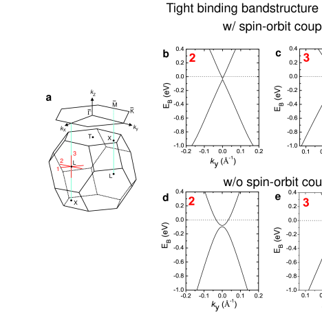
According to theoretical models, a strongly spin-orbit coupled bulk band structure is necessary for topological surface states to exist Fu:STI2 ; 11 ; 15 ; Roy; Murakami . Therefore it is important to show that our experimentally measured bulk band structure of Bi0.9Sb0.1 can only be accounted for by calculations that explicitly include a large spin-orbit coupling term. As shown in the previous section, the measured bulk band dispersion of Bi0.9Sb0.1 generally follows the calculated bulk bands of pure Bi from a tight binding model. The dispersion of the bulk valence and conduction bands of pure bismuth near at the point from such a tight binding calculation Liu with a spin-orbit coupling constant of 1.5 eV are shown in Fig. S3b and c, which show a high degree of linearity. The high degree of linearity can be understood from a combination of the large Fermi velocity ( 6 eV Å along ) and small inter-band (below ) gap = 13.7 meV (Fig. S3). This calculated inter-band gap of Bi (13.7 meV) is smaller than our measured lower limit of 50 meV (main text Fig. 2a) for the insulating gap of Bi0.9Sb0.1. To illustrate the importance of spin-orbit coupling in determining the band structure near , we show the dispersion along and calculated without spin-orbit coupling (Fig. S3d and e). While the dispersion along is not drastically altered by neglecting the spin-orbit coupling, the dispersion along changes from being linear to highly parabolic. This is further evidence that our measured Dirac point can be accounted for only by including spin-orbit coupling. A strong spin-orbit coupling constant acts as an internal quantizing magnetic field for the electron system Haldane(P-anomaly) which can give rise to a quantum spin Hall effect without any externally applied magnetic field Bernevig(QSHE); Sheng(QSHE) ; 8 ; Sheng . Therefore, the existence or the spontaneous emergence of the surface or boundary states does not require an external magnetic field.
VIII.7 Matching the surface state Fermi crossings and the topology of the surface Fermi surface in bulk insulating Bi0.9Sb0.1
In order to count the number of singly degenerate surface state Fermi crossings 14 ; 21 ; Kim along the -M̄ cut of the surface BZ, high photon energy ARPES scans, which allow mapping of the entire k range from -M̄ to fall within the detector window at the expense of lower instrument resolution, were taken to preliminarily identify the k-space locations of the Fermi crossings (Fig. S4a). Having determined where these surface state Fermi crossings lie in k-space, we performed several high resolution ARPES scans, each covering a successive small k interval in the detector window, in order to construct a high resolution band mapping of the surface states from to M̄. The second derivative image of the surface band dispersion shown in Fig.S4b was constructed by piecing together four such high resolution scans. Fig.S4c shows energy distribution curves of high resolution ARPES scans in the vicinity of each surface Fermi crossing, which together give rise to the surface Fermi surface shown. No previous work 14 ; Hochst ; Hofmann ; Hirahara ; Hengsberger ; Ast:Bi2 has reported the band dispersion near the -point (thus missing the Dirac bands) or resolved the Kramers point near the M̄ point, which is crucial to determine the topology of the surface states. For this reason there is no basis for one-to-one comparison with previous work, since no previous ARPES data exists in the analogous k-range. Note that surface band dispersions along the cuts A, B and C are highly linear. This is indirect evidence for the existence of the bulk Dirac point since surface states are formed when the bulk state wave functions are subjected to the boundary conditions at the cleaved plane.
VIII.8 Two-step fitting analysis procedure of Spin-Resolved ARPES measurements of insulating Bi1-xSbx
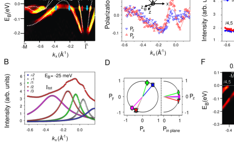
Here we present details of the spin-resolved ARPES analysis on bulk insulating Bi0.91Sb0.09 that show how we arrive at a spin-resolved surface band dispersion such as that presented in Figure 5(G) in the main text. In the VUV incident photon energy regime that we use, spin conserving photoemission processes (where the electric field of light only acts on the orbital degree of freedom of the electron inside a solid) dominate over spin non-conserving processes (which arise from coupling to the magnetic field of light) 33 . Therefore we are confident that the photo-emission process does not change the spin polarization of the electrons. Figure S5(B) shows a spin averaged momentum distribution curve (MDC) along the to -M̄ direction taken at = -25 meV, indicated by the green line shown in Figure S5(A). This MDC was obtained by summing the signal coming from both left and right electron detectors in the Mott polarimeter (see diagram in Fig.9(A) of the main text). Lorentzian lineshapes denoted and a non-polarized background are fitted to this MDC, which are used as inputs to the two-step fitting routine developed by Meier 26 in the following way. To begin with, a spin polarization vector is assigned to each band, where and are referenced to the primed Mott coordinate frame. Here it is necessary to assume a spin magnitude of one because only two spin components are measured by a single Mott detector. Such an assumption is likely valid since even though the spin polarization is no longer a good quantum number due to spin-orbit coupling, the bands near are expected to exhibit a high degree of spin polarization since the spin-orbit coupling is smallest near . Moreover, common strong spin-orbit coupled materials such as gold have been experimentally shown to exhibit 100% spin polarized surface states 18 . A spin-resolved spectrum is then defined for each peak using , where , and + and correspond to the spin direction being parallel () or antiparallel () to . The full spin-resolved spectrum is then given by , where is the unpolarized background, from which the spin polarization of each spatial component can be obtained as . This latter expression is a function of and and is used to fit to the experimental data.
The spin polarization data for the and components (i.e. and ) are obtained by taking the difference between the intensities of the left-right (or top-bottom) electron detectors over their sum, all divided by the Sherman function, which is calibrated using the methods in (31 , p.36). Typical electron counts on the detector reach , which places an error bar of approximately 0.01 for each point on our polarization curves. To account for unequal sensitivities between a detector pair, we applied a small multiplicative factor to the intensity from one detector to ensure that the unpolarized background intensity yields zero polarization. Resultant curves are shown in Figure S5(C). The best fit parameters (), which are expressed in the sample coordinates through an appropriate coordinate transformation [inset of Fig. S5(C)] are shown in Figure S5(D). Even though the measured polarization only reaches a magnitude of around 0.1, this is similarly seen in studies of Bi thin films 21 and is due to the non-polarized background and overlap of adjacent peaks with different spin polarization. These effects are extremely sensitive to the sample alignment due to the very narrow Fermi surface features. The fitted parameters [Fig. S5(D)] are consistent with spins being nearly aligned along the direction, with bands and having nearly opposite spin as required by time reversal symmetry, and with these spins nearly parallel to those of and respectively measured for Sb [main text Fig.9(F)]. The small departures from ideality likely originate from the scan direction not being exactly along -M̄. Bands and display opposite spin, which indicates that they form a Kramers pair split by spin-orbit coupling, and the fact that bands and have the same spin suggests that they originate from the same band.
To show that bands and connect above as we have drawn in Figure S5(A), and are thus expected to have the same spin, we map the surface band dispersion of Te doped Bi1-xSbx that is known to be an electron donor 35 . Figure S5(F) shows that the hole band formed by crossings 2 and 3 in insulating Bi1-xSbx [Fig. S5(A)] has sunk completely below with 0.5% Te doping, and is in fact the same band.
VIII.9 Method of using incident photon energy modulated ARPES to separate the bulk from surface electronic states of Sb
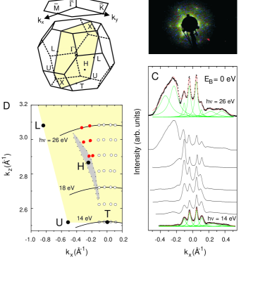
In this section we detail incident photon energy modulated ARPES experiments on the low lying electronic states of single crystal Sb(111), which we employ to isolate the surface from bulk-like electronic bands over the entire BZ. Figure S6(C) shows momentum distributions curves (MDCs) of electrons emitted at as a function of ( -M̄) for Sb(111). The out-of-plane component of the momentum was calculated for different incident photon energies () using the free electron final state approximation with an experimentally determined inner potential of 14.5 eV 37 ; 38 . There are four peaks in the MDCs centered about that show no dispersion along and have narrow widths of 0.03 Å-1. These are attributed to surface states and are similar to those that appear in Sb(111) thin films 37 . As is increased beyond 20 eV, a broad peak appears at -0.2 Å-1, outside the range of the surface states near , and eventually splits into two peaks. Such a strong dispersion, together with a broadened linewidth ( 0.12 Å-1), is indicative of bulk band behavior, and indeed these MDC peaks trace out a Fermi surface [Fig. S6(D)] that is similar in shape to the hole pocket calculated for bulk Sb near H 36 . Therefore by choosing an appropriate photon energy (e.g. 20 eV), the ARPES spectrum at along -M̄ will have contributions from only the surface states. The small bulk electron pocket centered at L is not accessed using the photon energy range we employed [Fig. S6(D)].
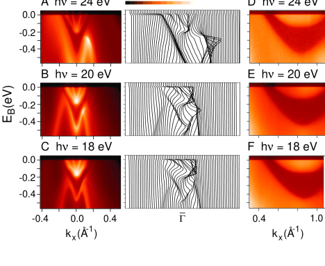
Now we describe the experimental procedure used to distinguish pure surface states from resonant states on Sb(111) through their spectral signatures. ARPES spectra along -M̄ taken at three different photon energies are shown in Fig. S7. Near there are two rather linearly dispersive electron like bands that meet exactly at at a binding energy -0.2 eV. This behavior is consistent with a pair of spin-split surface bands that become degenerate at the time reversal invariant momentum () due to Kramers degeneracy. The surface origin of this pair of bands is established by their lack of dependence on [Fig. S7(A)-(C)]. A strongly photon energy dispersive hole like band is clearly seen on the negative side of the surface Kramers pair, which crosses for 24 eV and gives rise to the bulk hole Fermi surface near H [Fig. S6(D)]. For 20 eV, this band shows clear back folding near -0.2 eV indicating that it has completely sunk below . Further evidence for its bulk origin comes from its close match to band calculations [Fig. S6(D)]. Interestingly, at photon energies such as 18 eV where the bulk bands are far below , there remains a uniform envelope of weak spectral intensity near in the shape of the bulk hole pocket seen with = 24 eV photons, which is symmetric about . This envelope does not change shape with suggesting that it is of surface origin. Due to its weak intensity relative to states at higher binding energy, these features cannot be easily seen in the energy distribution curves (EDCs) in Fig. S7(A)-(C), but can be clearly observed in the MDCs shown in Fig. S6(C) especially on the positive side. Centered about the M̄ point, we also observe a crescent shaped envelope of weak intensity that does not disperse with [Fig. S7(D)-(F)], pointing to its surface origin. Unlike the sharp surface states near , the peaks in the EDCs of the feature near M̄ are much broader (80 meV) than the spectrometer resolution (15 meV). The origin of this diffuse ARPES signal is not due to surface structural disorder because if that were the case, electrons at should be even more severely scattered from defects than those at M̄. In fact, the occurrence of both sharp and diffuse surface states originates from a dependent coupling to the bulk. As seen in Fig.7(D) of the main text, the spin-split Kramers pair near lie completely within the gap of the projected bulk bands near attesting to their purely surface character. In contrast, the weak diffuse hole like band centered near = 0.3 Å-1 and electron like band centered near = 0.8 Å-1 lie completely within the projected bulk valence and conduction bands respectively, and thus their ARPES spectra exhibit the expected lifetime broadening due to coupling with the underlying bulk continuum 39 .
VIII.10 Method of counting spin Fermi surface enclosures in pure Sb
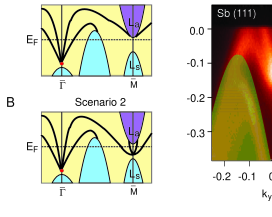
In this section we give a detailed explanation of why the surface Fermi contours of Sb(111) that overlap with the projected bulk Fermi surfaces can be neglected when determining the class of the material. Although the Fermi surface formed by the surface resonance near M̄ encloses the M̄, we will show that this Fermi surface will only contribute an even number of enclosures and thus not alter the overall evenness or oddness of enclosures. Consider some time reversal symmetric perturbation that lifts the bulk conduction La band completely above so that there is a direct excitation gap at L. Since this perturbation preserves the energy ordering of the La and Ls states, it does not change the class. At the same time, the weakly surface bound electrons at M̄ can evolve in one of two ways. In one case, this surface band can also be pushed up in energy by the perturbation such that it remains completely inside the projected bulk conduction band [Fig. S8(A)]. In this case there is no more density of states at around M̄. Alternatively the surface band can remain below so as to form a pure surface state residing in the projected bulk gap. However by Kramers theorem, this SS must be doubly spin degenerate at M̄ and its FS must therefore enclose M̄ twice [Fig. S8(B)]. In determining for semi-metallic Sb(111), one can therefore neglect all segments of the FS that lie within the projected areas of the bulk FS [Fig.7(G) of main text] because they can only contribute an even number of FS enclosures, which does not change the modulo 2 sum of enclosures.
In order to further experimentally confirm the topologically non-trivial surface band dispersion shown in figures 7(C) and (D) of the main text, we show ARPES intensity maps of Sb(111) along the -K̄K̄ direction. Figure S8(C) shows that the inner V-shaped band that was observed along the -M̄M̄ direction retains its V-shape along the -K̄K̄ direction and continues to cross the Fermi level, which is expected since it forms the central hexagonal Fermi surface. On the other hand, the outer V-shaped band that was observed along the -M̄M̄ direction no longer crosses the Fermi level along the -K̄K̄ direction, instead folding back below the Fermi level around = 0.1 Å-1 and merging with the bulk valence band [Fig. S8(C)]. This confirms that it is the band starting from that connects to the bulk valence (conduction) band, in agreement with the calculations shown in figure 7(D) of the main text.
VIII.11 Physical interpretation of : the mirror Chern number and an analogy with the spin-Chern number
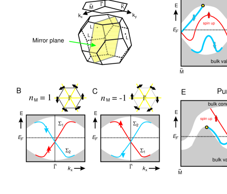
In this section we will describe how a mirror Chern number arises from the crystal symmetry of Bi1-xSbx. Electronic states in the mirror plane () [Fig. S9(A)] are eigenstates of the mirror operator with eigenvalues . is closely related to, but not exactly the same as the spin operator . It may be written as : the product of the parity operator and a twofold rotation operator : . For a free spin, does not affect the pseudovector spin, and simply rotates the spin. Thus, = exp. For spin eigenstates , this gives . In the crystal with spin-orbit interaction on the other hand, is no longer a good quantum number, but still is. The energy bands near the Fermi energy in Bi1-xSbx are derived from states with even orbital mirror symmetry and satisfy sign, as detailed in 20 and summarized below.
Unlike the bulk states which are doubly spin degenerate, the surface state spin degeneracy is lifted due to the loss of crystal inversion symmetry at the surface, giving rise to the typical Dirac like dispersion relations near time reversal invariant momenta [Fig. S9(B)&(C)]. For surface states in the mirror plane with , the spin split dispersion near has the form . Assuming no other band crossings occur, the sign of the velocity is determined by the topological mirror Chern number () describing the bulk band structure. When , the situation in figure S9(B) is realized where it is the spin up () band that connects the bulk valence to conduction band going in the positive direction (i.e. the spin up band has a velocity in the positive direction). For the opposite holds true [Fig. S9(C)]. These two possibilities also lead to two distinct chiralities of the central Fermi surface as shown in figures S9(B)&(C). From our spin-resolved ARPES data on both insulating Bi1-xSbx and pure Sb, we find that the surface polarized band dispersions are consistent with [Figs S9(D)&(E)], suggesting that their bulk electron wavefunctions exhibit the anomalous value predicted in (42), which is not realizable in free electron systems with full rotational symmetry.
There is an intimate physical connection between a 2D quantum spin Hall insulator and the 2D k-space mirror plane of a 3D topological insulator. In the former case, the occupied energy bands for each spin eigenvalue will be associated with an ordinary Chern integer , from which a non-zero spin-Chern number can be defined . In the latter case, it is the mirror eigenvalue of the occupied energy bands that have associated with them Chern integers , from which a non-zero mirror Chern number can be defined .
References
- (1) N. W. Ashcroft & N. D. Mermin, Solid State Physics (Holt, Rinehart and Winston, New York, 1976).
- (2) K. v. Klitzing, G. Dorda & M. Pepper, Phys. Rev. Lett. 45, 494 (1980).
- (3) D. C. Tsui, H. L. Stormer, & A. C. Gossard, Phys. Rev. Lett. 48, 1559 (1982).
- (4) R. B. Laughlin, Phys. Rev. Lett. 50, 1395 (1983).
- (5) X.-G. Wen, Int. J. Mod. Phys. B 4, 239 (1990).
- (6) D. J. Thouless , Phys. Rev. Lett. 49, 405 (1982).
- (7) J. E. Avron, D. Osadchy & R. Seiler, Phys. Today 56 (8), 38 (2003).
- (8) C. L. Kane & E. J. Mele, Phys. Rev. Lett. 95, 146802 (2005).
- (9) B. A. Bernevig, T. L. Hughes & S.-C. Zhang, Science 314, 1757 (2006).
- (10) L. Fu & C. L. Kane, Phys. Rev. B 76, 045302 (2007).
- (11) J. E. Moore & L. Balents, Phys. Rev. B 75, 121306(R) (2007).
- (12) L. Fu, C. L. Kane & E. J. Mele, Phys. Rev. Lett. 98, 106803 (2007).
- (13) M. König , Science 318, 766 (2007).
- (14) D. Hsieh , Nature 452, 970 (2008) [Completed and submitted in 2007]. Also see KITP Proceeding at http://online.itp.ucsb.edu/online/motterials07/hasan/ (2007).
- (15) Y. Xia ., Nature Phys. 5, 398 (2009). [Completed and submitted in 2008]. Preprint at http://aps.arxiv.org/abs/0812.2078 (2008).
- (16) D. Hsieh et al., Science 323, 919 (2009). [Completed and submitted in 2008].
- (17) D. Hsieh , Nature 460, 1101 (2009).
- (18) Y.L. Chen et al., Science 325, 178 (2009).
- (19) H. Zhang ., Nature Phys. 5, 438 (2009).
- (20) D. Hsieh ., Phys. Rev. Lett. 103, 146401 (2009).
- (21) L.A. Wray ., Nature Phys. 6, 855 (2010).
- (22) L.A. Wray ., Nature Phys. 7, 32 (2011).
- (23) S. Murakami, New. J. Phys. 9, 356 (2007).
- (24) B. Lenoir et al. Bi-Sb alloys: an update. Fifteenth International Conference on Thermoelectrics, 1-13 (1996).
- (25) Y. Liu & E. Allen, Phys. Rev. B52, 1566 (1995).
- (26) P. A. Wolff, J. Phys. Chem. Solids 25, 1057 (1964).
- (27) H. Fukuyama & R. Kubo, J. Phys. Soc. Jpn. 28, 570 (1970).
- (28) F. A. Buot, Phys. Rev. A8, 1570 (1973).
- (29) L. C. Hebel & G. E. Smith, Phys. Lett. 10, 273 (1964).
- (30) Y. Zhang et.al., Nature 438, 201 (2005).
- (31) S. Y. Zhou et al., Nature Mat. 6, 770 (2007).
- (32) F. D. M. Haldane, Phys. Rev. Lett. 61, 2015 (1988).
- (33) C. R. Ast & H. Hochst, Phys. Rev. Lett. 87, 177602 (2001).
- (34) H. Hochst & S. Gorovikov, J. Elect. Spectrosc. Relat. Phenom. 351, 144 (2005). This work does not measure the surface state along the critical direction or detect the bulk Dirac spectrum near L.
- (35) P. Hofmann, Prog. Surf. Sci. 81, 191 (2006).
- (36) T. Hirahara et al., Phys. Rev. B76, 153305 (2007).
- (37) M. Hengsberger et al. Eur. Phys. J. 17, 603 (2000).
- (38) C. R. Ast & H. Hochst, Phys. Rev. B67, 113102 (2003).
- (39) K. S. Novoselov et al., Science 315, 1379 (2007).
- (40) J. C. Y. Teo, L. Fu & C. L. Kane, Phys. Rev. B 78, 045426 (2008).
- (41) S. Hufner, Photoelectron Spectroscopy (Springer-. verlag, Berlin, 1995).
- (42) T. Hirahara , Phys. Rev. B 76, 153305 (2007).
- (43) J. J. Sakurai, Modern Quantum Mechanics (Addison-Wesley, New York, 1994).
- (44) X. -L. Qi, T. Hughes & S. -C. Zhang, Phys. Rev. B 78, 195424 (2008).
- (45) F. Meier , Phys. Rev. B 77, 165431 (2008).
- (46) M. Hoesch , Phys. Rev. B 69, 241401(R) (2004).
- (47) K. Sugawara , Phys. Rev. Lett. 96, 046411 (2006).
- (48) M. Hoesch , J. Electron Spectrosc. Relat. Phenom. 124, 263 (2002).
- (49) T. J. Gay & F. B. Dunning, Rev. Sci. Instrum. 63, 1635 (1992).
- (50) S.-Y. Xu , Science 332 560 (2011).
- (51) L. Fu & C. L. Kane, Phys. Rev. Lett. 100, 096407 (2008).
- (52) P. J. Leek , Science 318, 1889 (2007).
- (53) A. Kitaev, Ann. Phys. (NY) 303, 2 (2003).
- (54) Y. S. Hor ., Phys. Rev. B 81, 195203 (2010).
- (55) Y. Xia ., e-print arXiv:0812.2078 (2008).
- (56) M. Hoesch, PhD dissertation, University of Zürich, (2002).
- (57) S. Bengió et al., Surface Science 601, 2908 (2007).
- (58) P. D. Johnson. Rep. Prog. Phys. 60, 1217 (1997).
- (59) Y. Kopelevich , Phys. Rev. B 73, 165128 (2006).
- (60) A. Bostwick, T. Ohta, T. Seyller, K. Horn & E. Rotenberg, Nature Phys. 3, 36 (2007).
- (61) G. Jezequel, J. Thomas & I. Pollini, Phys. Rev. B 56, 6620 (1997).
- (62) C. R. Ast & H. Hochst, Phys. Rev. B 70, 245122 (2004).
- (63) D. N. Sheng, Z. Y. Weng, L. Sheng & F. D. M. Haldane, Phys. Rev. Lett. 97, 036808 (2006).
- (64) L. Sheng, D. N. Sheng, C. S. Ting & F. D. M. Haldane, Phys. Rev. Lett. 95, 136602 (2005).
- (65) T. K. Kim ., Phys. Rev. B 72, 085440 (2005).
- (66) D. M. Brown & S. J. Silverman, Phys. Rev. 136, A290 (1964).
- (67) L. M. Falicov & P. J. Lin, Phys. Rev. 141, 562 (1965).
- (68) H. Höchst & C. R. Ast, J. Electron Spectrosc. Relat. Phenom. 137, 441 (2004).
- (69) X. Gonze et al., Phys. Rev. B44, 11023 (1991).
- (70) E. Kneedler, K. E. Smith, D. Skelton & S. D. Kevan, Phys. Rev. B44, 8233 (1991).