Study of the optimal conditions for NV- center formation in type 1b diamond, using photoluminescence and positron annihilation spectroscopies.
Abstract
We studied the parameters to optimize the production of negatively-charged nitrogen-vacancy color centers (NV-) in type 1b single crystal diamond using proton irradiation followed by thermal annealing under vacuum. Several samples were treated under different irradiation and annealing conditions and characterized by slow positron beam Doppler-broadening and photoluminescence (PL) spectroscopies. At high proton fluences another complex vacancy defect appears limiting the formation of NV-. Concentrations as high as cm-3 of NV- have been estimated from PL measurements. Furthermore, we inferred the trapping coefficient of positrons by NV-. This study brings insight into the production of a high concentration of NV- in diamond, which is of utmost importance in ultra-sensitive magnetometry and quantum hybrid systems applications.
pacs:
81.05.ug, 61.72.jn, 61.72.jd, 61.72.Cc, 78.70.BjI Introduction
Owing to its unique properties of perfect photoluminescence stability and optically detectable electronic spin resonance with a long coherence time, the nitrogen-vacancy (NV-) color center in diamond has been the object of a large number of studies over the past few years Awschalom et al. (2007); Jelezko and Wrachtrup (2011) from quantum information processing, to highly sensitive magnetometry Balasubramanian et al. (2008); Taylor et al. (2008) and cellular imaging Chang (2010). Most of these studies rely on the properties of isolated single centers, but some applications can benefit from a high density of NV- centers while keeping a long spin coherence Stanwix et al. (2010), e.g. the realization of collective quantum memories Imamoğlu (2009), hybrid quantum circuits in which superconducting qubits are coupled to NV- electron spins Kubo et al. (2010), as well as ultrasensitive magnetometry at the micrometer scale Acosta et al. (2010); Taylor et al. (2008). Furthermore, the application of diamond nanoparticles as labels for bio-imaging also requires a high NV- content Chang et al. (2008); Faklaris et al. (2010). A well-known route to produce a high concentration of NV- centers is the irradiation by high-energy particles and the subsequent annealing of nitrogen-rich diamond.
In this work we determined the optimal parameters for the production of such a high NV- concentration. Several type 1b diamond samples were irradiated with 2.4 MeV protons at fluences ranging from 1012 to 1017 cm-2, and annealed under vacuum at temperatures from 600∘C to 1000∘C for durations from 1 to 20 hours. Each sample was characterized at different stages of the NV- formation process (before/after irradiation and after annealing) using photoluminescence (PL) spectroscopy and slow positron beam based Doppler-broadening spectrometry, referred in short as Positron annihilation spectroscopy (PAS). The latter technique provides information about the nature of the vacancy defects produced along the depth probed by the positrons Krause-Rehberg and Leipner (1999); Note (1).
II Experimental Procedure
The samples used are one-side polished mm3 type 1b HPHT diamond plates (Element Six Ltd.) with a nitrogen concentration specified below 200 ppm ( cm-3). Sample irradiation was performed with a 2.4 MeV proton scanning beam from a Van de Graff accelerator. During irradiation, the temperature of samples was maintained below 80∘C using a water-cooled sample holder. SRIM simulations111See supplementary material online. show that such protons create an almost constant concentration of atomic displacements in the first 25 m beneath the surface and stop at about 35 m producing cascades, which increase sharply the local damage concentration. The sample annealing was performed under vacuum. PL measurements were done with a confocal microscope equipped with an imaging spectrograph. We estimate the NV- concentration by quantitative comparison of the emission spectrum to the one of a single color centerNote (1).
For PAS measurements we used an accelerator delivering monoenergetic positrons with energy varying from 0.1 to 25 keV (for a complete description see Ref. Desgardin et al. (2001)). A Doppler broadening spectrometer coupled to the positron accelerator allows us to measure the energy of the gamma photon emitted from the electron-positron annihilation and hence to probe the vacancy defects. We determined the usual PAS parameters: (resp. ) corresponds to the annihilation fraction of low (respectively high) momentum electron-positron pairs, probing predominantly valence (respectively core) electrons Note (1). and change with an increase in the vacancy defect concentration or with a change in the nature of the defects probed. The measurements of and as a function of the positron energy allow to probe the sample as a function of the depth in the first 5 m under the surface.
III Results and discussions
PAS and PL measurements were first performed on untreated as-received diamond samples, then on irradiated but not annealed samples, and finally on irradiated and annealed ones.
For all PAS measurements presented in this work, the positron annihilation characteristics and as a function of the positron incident energy , can be viewed as resulting from a combination of surface and bulk characteristics. and exhibit plateaus at high positron energy (12-25 keV) (see Fig. 1(b)-(c) and inset of Fig. 2(a)), indicating that the contribution of the surface can be considered as negligible at the corresponding depths m and hence values are solely those of the bulk. From now on, we shall only refer to these plateau values and we consider that the distribution of vacancies is homogeneous in the region probed by the positrons.
III.1 Photoluminescence and positron annihilation measurements done on as-received samples
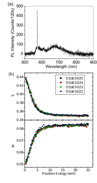
Figure 1(a) shows that the as-received sample exhibits a sharp PL peak at around 573 nm corresponding to the first order Raman peak of pure diamond at the excitation wavelength of 532 nm. A broader peak around 690 nm indicates the presence of native NV- color centers. A concentration of cm-3 of native NV- is estimated from the integration of this peak Note (1).
PAS measurements conducted on four different untreated samples show similar and graphs (Fig. 1(b)-(c)), indicating the homogeneity of diamond quality in the set of samples with respect to the atomic structures to which the positrons are sensitive. From these measurements, we inferred: and .
A fit of the data using VEPFIT Note (1) allows us to deduce a positron effective diffusion length, , of about 150 nm. This value is comparable to the value of 111 nm, which was found for in type 1b diamond Fischer et al. (1999). This shows that we can consider the bulk annihilation characteristics measured in the as-received samples as those of the pure diamond lattice . This implies that the concentration of vacancy-related defects present in the untreated type 1b samples is below the sensitivity threshold of the PAS technique corresponding to a value of about cm-3 [Fig. 5(b)].
Moreover, in the following, we will only consider the relative values and which are less sensitive to the experimental setup.
III.2 Photoluminescence and positron annihilation measurements done after irradiation and prior to thermal annealing
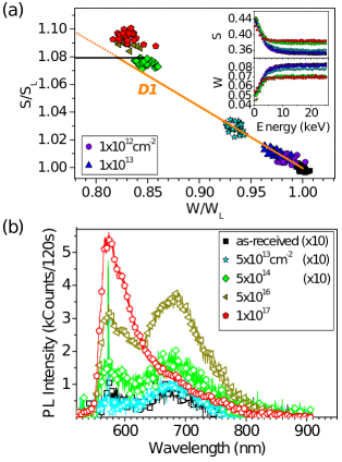
III.2.1 Photoluminescence measurements and inferred NV- color centers concentration
PL measurements done on samples irradiated at different proton fluences [Fig. 2(b)] display a broadband around 690 nm due to NV- photoluminescence and a higher energy PL band cut below 550 nm by the dichroic beamsplitter. This band is barely visible at the lowest fluence but becomes predominant at the highest fluences. It is tentatively attributed to the H3 (N-V-N) center emission Zaitsev (2001). The absence of the GR1 center emission (around 741 nm) associated to the neutral monovacancy is noteworthy. It has been shown that in type 1b diamond the monovacancy is preferentially in the negative charge state Davies et al. (1992) due to the presence of the nitrogen impurity, which can donate an electron to the monovacancy. Both charge states coexist when there are not enough nitrogen donors with respect to vacancies. For the fluence cm-2 the maximal vacancy concentration can be estimated by that of the atomic displacements calculated by SRIM Note (1) to be cm-3, which is larger than the specified nitrogen concentration cm-3. The absence of the GR1 line therefore indicates that the real monovacancy concentration is lower than the one of atomic displacements, as a result of vacancy-interstitial recombination or non-photoluminescent complex vacancy formation.
III.2.2 Positron annihilation measurements
Figure 2 (a) shows that when we increase the fluence, increases and decreases indicating the formation of vacancy defects. For fluences cm-2, the data are well fitted by a straight line D1 starting from the as-received sample measurements. This line is the signature of an annihilation state additional to the lattice one and consecutive to irradiation. Since the annihilation fraction in this state increases with the fluence, we suggest that it corresponds to the negatively charged monovacancy, which is the most simple defect that can be created in this type of nitrogen-rich diamond Pu et al. (2000).
For fluences cm-2 the points are located above D1, indicating that a new type of vacancy-related defect appears Liszkay et al. (1994). This claim is supported by the fact that we measure larger relative changes of values than the one of the neutral or negative monovacancy in diamond Pu et al. (2000) ( and ) indicated by the horizontal black line in Fig. 2 (a)222Interestingly, we can also estimate from the intersection of this monovacancy horizontal line with D1. In order to check if NV- corresponds to this defect center, we estimated its highest concentration from the PL spectrum [Fig. 2(b)], to be cm-3 at fluence cm-2. Such a NV- concentration is hardly detectable by PAS as proved by further measurements on annealed samples [Fig. 5(b)]. Moreover this concentration is over-estimated due to the contribution of the high-energy band in the PL spectrum. Therefore NV- centers present in the samples after irradiation but prior to annealing can only marginally contribute to the shift. This deviation to the D1 observed at the highest fluences is most likely related to multiple vacancy defects.
III.3 Post-thermal annealing studies
III.3.1 NV- center formation at fixed proton fluence of cm-2 and various annealing conditions
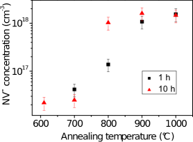
To investigate the effect of annealing time and temperature, diamond samples were irradiated at a proton fluence of cm-2 and annealed at temperatures ranging from 600∘C to 1000∘C, during 1 or 10 hours. Figure 3 displays the estimated NV- concentration for the different conditions. A significant increase in the NV- concentration above 700∘C is observed. Furthermore [NV-] saturates at cm-3. Note that from 800∘C to 1000∘C, the difference in NV- concentration for the two annealing times becomes smaller, eventually vanishing at 1000∘C. The NV- formation kinetics is thus enhanced upon temperature increase.
III.3.2 NV- center formation for fixed annealing conditions (800∘C, 20 hours) and various fluences
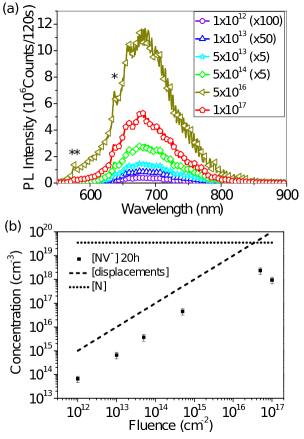
We also studied the influence of the irradiation fluences (from cm-2 to cm-2) on NV- center formation for a given annealing condition (800∘C, 20 hours). The PL spectra of Fig.4(a) show an intensity increase with the fluence up to cm-2. Yet at all the fluences, the inferred NV- concentration plotted on Fig. 4(b) is one order of magnitude lower than that of the atomic displacements predicted by SRIM, probably due to vacancy-interstitial recombination. The maximum NV- concentration reached is cm-3. Note that a lower NV- concentration is measured for the highest fluence. This decrease could have been attributed to the onset of diamond amorphization but confocal Raman spectroscopy did not reveal any sp2 carbon signal Note (1). However, PAS measurements provides an explanation as shown in the next paragraph.
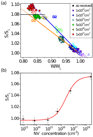
Figure 5(a) displays for the different fluences before and after annealing. At all the fluences, we observe a decrease of concomitant with an increase of after annealing, indicating that the vacancy defect concentration diminishes and/or the nature of the defects changes. points after annealing are aligned on a new straight line D2 except the highest fluence one. Since PL measurements evidence the creation of NV- defect, we propose that it is the defect associated to D2. This claim is supported by previous work showing an increase of due to nitrogen decoration of vacancies in diamond Sachdeva et al. (2004). Note that for cm-2 and cm-2 fluences points which are initially off the monovacancy D1 line finally end onto D2 after annealing. It could be due to the positron trapping rate balance between different vacancy traps shifting the and values to the annihilation characteristics of the NV- vacancy defect which has a high trapping coefficient, without excluding that annealing can partially remove the complex vacancies. In contrast, for the highest fluence the points almost did not move after annealing, and still fall off the D2 line, which indicates that there is a significant fraction of complex vacancies that do not evolve into NV- centers, thus limiting the NV- creation yield. It would be worthwhile to anneal at temperatures higher than 1000∘C. This strategy was successful in increasing the NV- electronic spin coherence as a result of paramagnetic defect destruction Naydenov et al. (2010) including divacancies associated ones like R4 or W6 Twitchen et al. (1999).
III.3.3 Trapping coefficient of positrons by NV- suggested by positron annihilation and photoluminescence measurements
The combination of PAS and PL measurements also allows us to estimate the trapping coefficient of positrons by NV-. Fig. 5(b) displays as a function of the NV- concentration inferred from PL spectra [Fig. 4(a)]. The data can be fitted by a relationship derived from rate equations Pu et al. (2000) considering the lattice and vacancy defects (mostly NV-) as the positron trapping sites:
| (1) |
where is the lattice annihilation rate, and cm-3 the NV- center concentration and diamond lattice atomic density respectively. is the associated positron trapping rate. Taking ns-1 from Ref. Pu et al. (2000), the best fit to the data is obtained for and s-1. The same type of fit can be performed for , yielding and s-1. The two values of obtained are consistent, and we take their mean value s-1 as the one inferred from PAS. In silicon the positron trapping coefficient has been found to be s-1 for the neutral divacancy Mascher et al. (1989) and s-1 for the (VP)- defect Kawasuso et al. (1995). The more efficient trapping of V- in diamond compared to (VP)- in silicon can be explained by: (1) a smaller static dielectric constant (5.6 for diamond and 11.6 for silicon), hence a longer range coulomb potential in the case of diamond, (2) a binding energy of 0.3 eV for the Rydberg state of the V- electron, larger than the one of 0.1 eV in silicon, leading to a significant reduction of the positron detrapping in diamond. Table 1 summarizes the PAS data related to the defects detected in this work.
| Positron parameters | V- | NV- |
|---|---|---|
| Pu et al. (2000) | ||
| s | - |
IV Conclusion
We have optimized the formation of a high-density of NV- centers in type 1b diamond by proton irradiation and subsequent thermal annealing. We showed that the conversion efficiency of nitrogen into NV- increases with the irradiation fluence, up to a point where further increase leads to a reduction in this conversion rate, most likely due to the creation of complex vacancies stable under 800∘/20 h annealing. We achieved the maximum NV- concentration of cm-3 (13.5 ppm), corresponding to a conversion efficiency [NV-]/[N] of about 6.7% ([N] ppm). The positron trapping coefficient by NV- centers in diamond was estimated for the first time.
Acknowledgement
We thank J.-F. Roch, V. Jacques and A. Trifonov for fruitful discussions, and M.-R. Ammar for help in Raman measurements. This work was supported by the French National Research Agency (ANR-07-NANO-045).
References
- Awschalom et al. (2007) D. D. Awschalom, R. Epstein, and R. Hanson, Scientific American 297, 84 (2007).
- Jelezko and Wrachtrup (2011) F. Jelezko and J. Wrachtrup, New J. Phys. 13 (2011).
- Balasubramanian et al. (2008) G. Balasubramanian, I. Y. Chan, R. Kolesov, M. Al-Hmoud, J. Tisler, C. Shin, C. Kim, A. Wojcik, P. R. Hemmer, A. Krueger, T. Hanke, A. Leitenstorfer, R. Bratschitsch, F. Jelezko, and J. Wrachtrup, Nature 455, 648 (2008).
- Taylor et al. (2008) J. M. Taylor, P. Cappellaro, L. Childress, L. Jiang, D. Budker, P. R. Hemmer, A. Yacoby, R. Walsworth, and M. D. Lukin, Nature Phys. 4, 810 (2008).
- Chang (2010) H.-C. Chang, Nanodiamonds, edited by D. Ho (Springer, 2010).
- Stanwix et al. (2010) P. L. Stanwix, L. M. Pham, J. R. Maze, D. Le Sage, T. K. Yeung, P. Cappellaro, P. R. Hemmer, A. Yacoby, M. D. Lukin, and R. L. Walsworth, Phys. Rev. B 82, 201201 (2010).
- Imamoğlu (2009) A. Imamoğlu, Phys. Rev. Lett. 102, 083602 (2009).
- Kubo et al. (2010) Y. Kubo, F. R. Ong, P. Bertet, D. Vion, V. Jacques, D. Zheng, A. Dréau, J. F. Roch, A. Auffeves, F. Jelezko, J. Wrachtrup, M. F. Barthe, P. Bergonzo, and D. Esteve, Phys. Rev. Lett. 105, 140502 (2010).
- Acosta et al. (2010) V. M. Acosta, E. Bauch, A. Jarmola, L. J. Zipp, M. P. Ledbetter, and D. Budker, Appl. Phys. Lett. 97, 174104 (2010).
- Chang et al. (2008) Y.-R. Chang, H.-Y. Lee, K. Chen, C.-C. Chang, D.-S. Tsai, C.-C. Fu, T.-S. Lim, Y.-K. Tzeng, C.-Y. Fang, C.-C. Han, H.-C. Chang, and W. Fann, Nature Nanotech. 3, 284 (2008).
- Faklaris et al. (2010) O. Faklaris, J. Botsoa, T. Sauvage, J.-F. Roch, and F. Treussart, Diam. Relat. Mater. 19, 988 (2010).
- Krause-Rehberg and Leipner (1999) R. Krause-Rehberg and H. S. Leipner, Positron Annihilation in Semiconductors: Defect Studies, Solid-State Sciences, Vol. 127 (Springer Verlag, Berlin, 1999).
- Note (1) See supplementary material online.
- Desgardin et al. (2001) P. Desgardin, L. Liszkay, M. F. Barthe, L. Henry, J. Briaud, M. Saillard, L. Lepolotec, C. Corbel, G. Blondiaux, A. Colder, P. Marie, and M. Levalois, Mater. Sci. Forum 363-365, 523 (2001).
- Fischer et al. (1999) C. Fischer, S. Connell, P. Coleman, F. Malik, D. Britton, and J. Sellschop, Applied Surface Science 149, 221 (1999).
- Zaitsev (2001) A. Zaitsev, Optical Properties of Diamond (Springer, 2001).
- Davies et al. (1992) G. Davies, S. C. Lawson, A. T. Collins, A. Mainwood, and S. J. Sharp, Phys. Rev. B 46, 13157 (1992).
- Pu et al. (2000) A. Pu, T. Bretagnon, D. Kerr, and S. Dannefaer, Diam. Relat. Mater. 9, 1450 (2000).
- Liszkay et al. (1994) L. Liszkay, C. Corbel, L. Baroux, P. Hautojärvi, M. Bayhan, A. W. Brinkman, and S. Tatarenko, Appl. Phys. Lett. 64, 1380 (1994).
- Note (2) Interestingly, we can also estimate .
- Waldermann et al. (2007) F. Waldermann, P. Olivero, J. Nunn, K. Surmacz, Z. Wang, D. Jaksch, R. Tyalor, I. Walmsley, M. Dragansky, and P. Reichart, Diam. Relat. Mater. 16, 1887 (2007).
- Sachdeva et al. (2004) A. Sachdeva, K. Sudarshan, P. Pujari, A. Goswami, K. Sreejith, V. George, C. Pillai, and A. Dua, Diam. Relat. Mater. 13, 1719 (2004).
- Naydenov et al. (2010) B. Naydenov, F. Reinhard, A. Lämmle, V. Richter, R. Kalish, U. F. S. D’Haenens-Johansson, M. Newton, F. Jelezko, and J. Wrachtrup, Appl. Phys. Lett. 97, 242511 (2010).
- Twitchen et al. (1999) D. Twitchen, M. Newton, J. Baker, T. Anthony, and W. Banholzer, Appl. Phys. Lett. 59, 12900 (1999).
- Mascher et al. (1989) P. Mascher, S. Dannefaer, and D. Kerr, Phys. Rev. B 40, 11764 (1989).
- Kawasuso et al. (1995) A. Kawasuso, M. Hasegawa, M. Suezawa, S. Yamaguchi, and S. Sumino, Jpn. J. Appl. Phys. 34, 2197 (1995).