Coherent transport through graphene nanoribbons in the presence of edge disorder
Abstract
We simulate electron transport through graphene nanoribbons of experimentally realizable size (length up to m, width nm) in the presence of scattering at rough edges. Our numerical approach is based on a modular recursive Green’s function technique that features sub-linear scaling of the computational effort with . We investigate backscattering at edge defects: Fourier spectroscopy of individual scattering states allows us to disentangle inter-valley and intra-valley scattering. We observe Anderson localization with a well-defined exponential decay over 10 orders of magnitude in amplitude. We determine the corresponding localization length for different strength and shape of edge roughness.
pacs:
73.23.-b, 73.63.-b, 73.40.-cI Introduction
The experimental realization of graphene, i.e., of a monolayer of carbon atoms BerryGeim ; MasslessFirsov ; ElectricFirsov has opened up a rapidly developing field of fundamental and applied physics. The topology of the planar honeycomb lattice [figure 1(a)] with the resulting peculiar band structure near the and points [figure 1(b), for a review, see guinea_review ; dassarma_review ] gives rise to many novel and intriguing physical properties, including the room temperature quantum Hall effect, minimum conductivity at the Fermi energy as well as possible applications for spintronics. Recent advances in fabricating width-modulated graphene nanoribbons helped to overcome intrinsic difficulties in creating tunnelling barriers and confining electrons in graphene, where transport is dominated by Klein tunneling-related phenomena dom99 ; kat06 . Graphene quantum dots have been fabricated and Coulomb blockade sta08aa ; sta08ab ; pon08 , quantum confinement sch09 and charge detection gue08 have been demonstrated.
The electronic properties of the perfect honeycomb lattice are meanwhile theoretically well understood guinea_review . However, in realistic graphene devices finite-size effects and imperfections play an essential role, especially for transport through confined structures. The importance of such effects results from the gapless band structure of graphene which does not allow straightforward confinement by electrostatic potentials. Devices thus have to be cut or etched resulting in rough edges. In turn, properties of the ideal graphene band structure cannot be invoked when simulating quantum transport through realistic devices in the presence of randomly shaped boundaries. Moreover, recent results underline that an incoherent Boltzmann transport approach, unlike a full quantum-mechanical calculation, fails to reproduce experimentally observed conductance signatures for impurity scattering Klos . However, the application of numerical methods for a full quantum mechanical simulation of graphene ribbons of realistic size constitutes a considerable challenge. A method of choice is the widely-used recursive Green’s function technique MacKinnon2 which is well suited to treat scattering structures such as wires or ribbons extended in one of their dimensions and usually implemented within the Landauer-Büttiker framework Ferry for calculating transport coefficients. This technique has meanwhile been incorporated successfully into both an equilibrium bara ; Lewenkopf ; Roche ; Heinzel ; tra07 and a non-equilibrium cres ; meta ; neop ; sviz (Keldysh) description. Several variants of this method have been put forward employing specific symmetries of the system sols ; PRB62RTWTB ; Stephan if applicable, or using recursive algorithms kazy ; wimm ; drou ; mama ; JoooSuper ; JoooSuper2 . In this article we present an extension of the modular recursive Green’s function method (MRGM)Stephan designed to treat graphene nano-ribbons with edge or bulk disorder. We address disorder scattering in graphene nanoribbons both on the microscopic level of specific lattice defects as well as on the macroscopic level of current measurements for which, as we will demonstrate, the details of the underlying disorder scattering play a crucial role.
This paper is organized as follows: We briefly review key properties of the band structure of “ideal” infinitely extended graphene in the absence of disorder in section II. In section III, we introduce the application of the MRGM to finite-size graphene structures which allows us to treat extended structures efficiently due to the favorable scaling of the numerical effort with the linear dimensions of the ribbon. Applications to transport through rough-edged graphene nanoribbons will be presented in section IV followed by a short summary (section V).
II Tight-binding simulation of graphene band structure
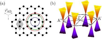
The ideal, infinitely extended graphene sheet features a honeycomb lattice made up of two (A and B) interleaved triangular sublattices. It can be described in tight-binding (TB) approximation by the Hamiltonian Wallace
| (1) |
where the sum extends over pairs of lattice sites, is the tight-binding orbital with spin at lattice site , is a locally varying potential (onsite energy), and is the hopping matrix element between lattice sites and . Within our TB approximation, we include third-nearest-neighbour coupling [see figure 1(a)] using orthogonal tight-binding orbitals. This allows for four free parameters, namely the site-energy and the overlap integrals , , representing the interaction with the first, second and third nearest neighbour, respectively. We choose the by fitting to ab-initio calculations, taken from Reich et al. TBReich ; Grueneis ; LibPRB08 , arriving at , , and .
The dispersion near the non-equivalent and points [figure 1(b)] resulting from the diagonalization of equation (1) features [for large distances from ()] deviations from a perfect cone reflecting the influence of the hexagonal lattice. The cone becomes squeezed along the directions, an effect known as trigonal warping McCann06b ; guinea_review . Near the point and for small the band structure of equation (1) can be approximated (assuming that ) by a conical dispersion relation around the point Semenoff ,
| (2) |
where we have set . Note that the above expansion ignores both the length scale of the graphene lattice constant Å and the preferred directions of the lattice due to the discrete lattice symmetry. In this low- limit, the Hamiltonian, equation (1), can be approximated by the Dirac Hamiltonian,
| (3) |
with and being the Pauli spin matrices acting on the pseudo-spin and valley degrees of freedom. Analytic solutions for an infinitely extended graphene sheet described by equation (3) yields plane waves where the angle of the vector ,
| (4) |
connects relative amplitudes on the and sublattice guinea_review ,
| (5) |
Consequently, the pseudo-spin projection along the direction of propagation, the “helicity”,
| (6) |
is conserved reflecting the chiral symmetry of the ideal graphene sheet in the low- limit. The additional degeneracy of two non-equivalent cones (“valleys”) at the and points in the reciprocal lattice allows to formally represent the low-energy band structure near in terms of Dirac-like four-spinors with amplitudes for the sublattice in real space and in reciprocal space. The sign of [equation (4)] is reversed upon transition from to . (Note that physical spin is not included in the present analysis.)
This Dirac-like picture may serve as valuable starting point for the analysis of finite-size and edge effects on transport incorporated within the tight-binding Hamiltonian [equation (1)]. Chirality [equation (6)] is preserved in the presence of slowly (on the scale of the C-C bondlength) varying perturbations, suppressing backscattering guinea_review
| (7) |
Conversely, rough edges may break chirality resulting in non-vanishing backscattering on the same cone and, at the same time, in coupling of the and cones. In the following, we will investigate in detail the effects of short-range defects Ugeda (e.g. edges) and deviations from the continuum Dirac picture on the transport properties of rough-edged graphene nanoribbons.
III Numerical Method
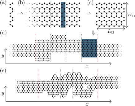
For the numerical treatment of finite-size graphene flakes and ribbons a number of simulation algorithms have meanwhile been proposed MacKinnon2 ; bara ; Lewenkopf ; Heinzel ; tra07 ; cres ; meta ; neop ; sviz ; Roche . We use in the following an extension of the Modular Recursive Green‘s function Method (MRGM) PRB62RTWTB ; Stephan ; Rott06 applied to the third-order TB Hamiltonian [equation (1)]. The key idea of the MRGM is to break down a large device into independent smaller modules, each of which can be computed efficiently [see figure 2]. The Green’s functions of the different modules with width and length are then combined to the desired device geometry using a small number of Dyson equations. In this Article, we introduce an efficient method to calculate the : the associated numerical effort becomes independent of module length . The algorithm involves the somewhat counter-intuitive steps to first calculate infinitely and semi-infinitely extended ribbons, i.e., modules of width but , from which rectangular modules of finite length are “cut out” as needed by applying the Dyson equation “in reverse”. The obvious advantage of this approach is that the computational effort becomes independent of . This approach is particularly advantageous for the simulation of weakly disordered graphene nano-ribbons: for weak disorder the spacing between individual defects both in the bulk and at the edges of the ribbon is large as compared to the lattice spacing. We can thus simulate the region between neighbouring defects by a single graphene module with perfect boundaries and place adjacent defects at the module boundaries [see red dotted lines in figure 2(d)]. This efficient calculation of the extended rectangular modules in between two defects is key to simulating large devices with length up to several micrometers (or hexagons in one direction).
As a prototypical example, we build up an infinitely long nanoribbon with ideal zigzag boundaries (along the direction) by periodic repetition of a chain of carbon atoms of width in transverse () direction [see figure 2(a)]. Other geometries and boundaries can be treated analogously. The Hamiltonian of the ribbon can thus be decomposed into a matrix describing the Hamiltonian of the vertical chain, and the coupling matrix describing the connection between two adjacent chains Sanvito ,
| (8) |
The solution of the Schrödinger equation for the infinite ribbon can be written in terms of an ansatz for a Bloch wave
| (9) |
with the transverse eigenfunction. For expanding the Green’s function in terms of we need a complete set of transverse eigenfunctions including all evanescent modes in the sum [equation (9)] and the subsequent equations. The resulting generalized eigenvalue problem for and gives left (right)-moving states (), with corresponding momentum () in direction. In the following, we introduce the shorthand notation () for the projections onto the right (left) moving Bloch states. From the Bloch states the Green’s function of the infinite ribbon follows as Sanvito
| (10) |
with the hopping matrix
| (11) |
The Green’s function of the half-infinite ribbon extending from to (or can be written as
| (12) |
with
| (13) | |||||
| (14) |
satisfying the boundary conditions for all or located at the end of the half-infinite ribbon (). For an intuitive interpretation of equation (12) consider a disturbance from a point source at . It reaches by two paths: the direct propagation from to , given by the Green’s function of the infinite ribbon, and the propagation from to [given by in equation (14)], where the wave is reflected at the end of the ribbon and then propagates from to [given by in equation (14)]. Note that the numerical effort to calculate and is controlled by the transverse width of the ribbon and the number of transverse modes to be included while the -dependence is given analytically. This scaling behaviour is key to calculate for the rectangular ribbon of arbitrary length by solving the Dyson equation
| (15) |
in reverse for instead of for . Consequently, the numerical effort to calculate is independent of . In the final step, a rough-edged nanoribbon can now be assembled by successively joining rectangular ribbons of varying length and width (average width nm) using the Dyson equation in forward direction,
| (16) |
In our simulations, we treat ribbon lengths of several micrometers, and average over 100 random realizations of edge roughness to eliminate non-generic features of particular ribbon configurations. To assemble such very long disordered ribbons, we start with a set of different modules and combine them to obtain a larger module . We connect the calculated modules in a random permutation , (e.g., for , ). This procedure is repeated iteratively [i.e., , formally equivalent to the composition rule of a Fibonacci sequence], creating an exponentially growing, pseudo-random sequence of modules. The interfaces between modules that include the disorder are randomly determined at each iteration step to avoid periodic repetition.
If a more general shape of the scattering geometry is desired [e.g., for a non-separable disorder potential or curved boundaries, see figure 2(e)], the partitioning into modules and the subsequent efficient buildup of long structures is still readily possible. Only the first step of our algorithm has to be modified. The Green’s function of individual modules is directly calculated by inversion, i.e., , using, e.g., a parallelized sparse-matrix solver MUMPS . Subsequent application of Dyson equations allows to assemble complex scattering geometries.
We find that the computing time of our approach scales as due to the cubic dependence of the eigenvalue problem and of the matrix multiplications. scales linearly with the number of building blocks used to set up the geometry, and logarithmically with . Numerically, we find for ,
| (17) |
with given in nm. We have determined a prefactor from calculating the full scattering problem averaged over 100 configurations, when computing on 3 AMD Opteron processors (24 cores) at 2.2 GHz. Clearly, the prefactor strongly depends on the details of the employed hardware (i.e., network speed, cache size, compilation flags, etc.), while the scaling (17) does not.
We note that the application of the algorithm presented here is not restricted to graphene nanostructures: any modular scattering system, which is build from modules along the lines of figure 2 (a)-(c) can be treated analogously. Possible applications include acoustic cavities, conventional semiconductors, topological insulators, or neutron scattering devices.
IV Results
IV.1 Transport coefficients
For conventional semiconductor heterostructures (e.g., quantum dots made of GaAs-AlGaAs), confinement is usually achieved by electrostatic gates resulting in smooth dot boundaries. Such confinement is not realizable for graphene due to its gapless band structure. While several theoretical concepts for opening a band gap have been proposed, the majority of experiments have achieved confinement by patterning of graphene nanodevices with oxygen plasma etching, chemical vapor deposition, specially prepared SiC substrates deHeer , or chemical etching. These techniques, however, do not result in well-defined armchair or zigzag edges but in a rough-edge pattern featuring armchair and zigzag elements as well as adsorbates at the dangling carbon bonds pon08 ; sta08aa ; sta08ab ; KimNature leading to an irregular edge structure. Edge effects can thus be expected to strongly influence the properties of graphene nanodevices.
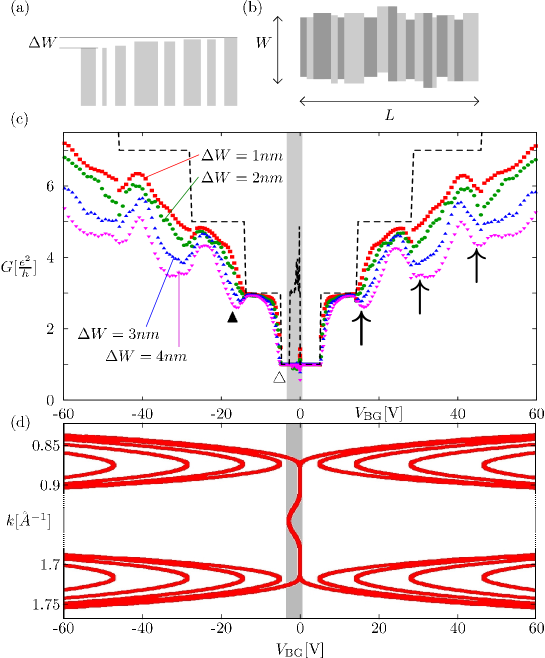
We simulate the influence of edge scattering on transport through graphene nanoribbons by randomly varying the widths of the rectangular modules which build up the ribbon in the range 1 nm [see figure 3(a)]. Numerical tests show that a random sequence of different module widths represents a good compromise between a high degree of randomness and limited computational effort. In order to suppress correlations in the -dependence of the roughness, the length of each rectangular module is chosen at random in the range of 0.24nm (one unit cell) to 10nm. We then use the above Fibonacci-like procedure to assemble a scattering geometry [see figure 3(b)] of up to several m in length. Finally, all modules are connected to two ideal half-infinite graphene waveguides. We average over 100 realizations of nanoribbons to eliminate non-generic features of particular ribbon configurations.
In addition to the quantization steps due to transverse confinement [dashed black line in figure 3(c)], a graphene nanoribbon with a perfect zigzag boundary of fixed width features edge states with finite dispersion [figure 3(d)] since the coupling between the outermost carbon atoms is non-zero dassarma_review . Consequently, the edge states of an ideal nanoribbon give rise to a peak in conductance just below the Dirac point [shaded area in figure 3(c,d)]. In contrast to first-nearest-neighbor tight binding, and in line with the full ab-initio bandstructure and experiment dassarma_review , our third nearest neighbor approach accounts for the breaking of electron-hole symmetry. Conductance is thus only approximately symmetric relative to .
In the presence of edge disorder, undergoes several pronounced changes [figure 3(c)]: overall, decreases with increasing distance in energy from the Dirac point relative to the ideal ribbon. The quantization steps due to the transverse confinement are strongly suppressed. Moreover, the edge disorder completely removes the sharp conductance peak attributed to edge states, as they are no longer conducting but become localized parallel to the ribbon LibPRB08 , i.e. along the direction of transport. Consequently, corresponding signatures are difficult to observe in transport measurements of realistic samples. Scanning tunneling spectroscopy provides an alternative approach: peaks in the local density of states at energies slightly below the Dirac point have been recently, indeed, observed in STS experiments niimi .
In the limit where quantization steps due to the transverse confinement are strongly suppressed [figure 3(c)] pronounced broad dips in transmission (see arrows in figure 3) replace the original steps in conductance. This counter-intuitive reduction of transmission with increasing energy in the vicinity of steps can be qualitatively understood by considering Fermi’s golden rule for the scattering of mode into mode Ihnatsenka ; LibKirchberg2011 ,
| (18) |
Two trends contribute to this effect: firstly, strong fluctuations of the ribbon width broaden the DOS and smoothen the steps. Secondly, as the ribbon locally narrows, backscattering via scattering into evanescent modes is enhanced. This occurs preferentially for energies close to the opening of a new mode and results in a reduction in transmission causing the dips.
It is instructive to compare the present results to calculations for edge- and bulk- disordered semiconductor nanowires featuring a parabolic dispersion relation in the long-wavelength (continuum) limit. While a reduction of quantization steps by disorder is observed for edge-disordered semiconductor ribbons Nikolic1994 resembling the present results, the prominent transmission dips observed for graphene (arrows in figure 3) appear not to be present in such a system (compare with figure 2 in Nikolic1994 ). However, dips have been found in other disordered semiconductor nanostructures that are associated with resonances supported by attractive (bulk) disorder potentials Bagwell . The distance in energy between these resonances and the quantization step (i.e. the subband minimum) corresponds to the binding energy of the (quasi) bound state Bagwell . In the present case of graphene with rough edges, the enhancement of the local density of states near the Dirac point resulting from localized states at the edges is well known Heinzel . Their statistical weight has been found to be much higher for graphene than for conventional nanostructures LibPRB08 . In the absence of a local attractive potential, these localized states could take on the role of resonances: for edge structures similar to the ones we investigate, the resonance energies are statistically distributed in the range meV LibPRB08 , and could, possibly, give rise to the observed broad dips.
IV.2 Localized scattering states at edges
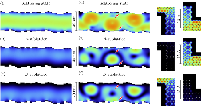
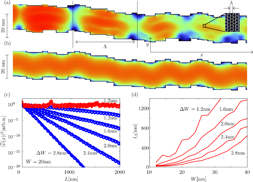
To gain a deeper understanding of the transport characteristics of edge-disordered graphene ribbons, we now analyze also individual scattering states. We find that states with energies where the conductance is only weakly perturbed by edge disorder [e.g. open triangle in figure 3(c)] feature a low amplitude at the edges [see figure 4(a)]. The overall probability density of these scattering states remains concentrated near the center of the ribbon [see figure 4(a)] and is therefore only slightly affected by edge disorder. When only a single mode is open in the leads (at energies close to the Dirac point), modes located at and in momentum space are not coupled in a zigzag graphene nanoribbon guinea_review . Only one cone contributes to transport in each direction [see figure 3(d)]. This imbalance in the number of left- and right-moving channels on each cone is a special property of zigzag graphene nanoribbons Wakaba , similar to the band structure of topological insulators. Backscattering is only possible in this energy window by inter-valley scattering at the rough edges. Since we observe a nearly perfectly conducting channel [figure 5(b),(c)], inter-valley scattering that requires momentum transfers of the order is obviously suppressed at low energies XiongA .
By contrast, scattering states at energies where transmission (and conductance) is considerably reduced [solid triangle in figure 3(c) and figure 4(b)] feature a strong enhancement of their wavefunction near corners of the edges originating from one sub-lattice only [see arrows in figure 4(e, f)]. Projections onto the and sublattices [figure 4 (e, f)] show pronounced differences reflecting the violation of pseudo-spin conservation [equation (7)]. We find enhancements of the () sub-lattice scattering wave function at the upper (lower) edges of the ribbon, i.e., at those edges where the outermost carbon atom is of type () [see zoom-ins in figure 4(d)-(f)], in line with a strong enhancement of the local DOS near rough edges Heinzel ; guinea_review ; dassarma_review . However, the pronounced differences in the wavefunction patterns near the center of the ribbon are not accounted for only by localized edge states since their decay length into the ribbon interior is much smaller than the ribbon width. We therefore attribute the dramatic drop in conductance to pronounced intra-valley and inter-valley backscattering at the edge corners, since the suppression of backscattering associated with the conservation of pseudo-spin [equation (7)] no longer holds.
As reported in earlier work on edge disorder in rough-edged graphene nanoribbons, transmission is strongly suppressed close to the Dirac point, leading to the formation of a transport gap Lewenkopf ; Heinzel . Atomic-scale defects on the edges of wide ribbons may lead to exponential (i.e., Anderson) localization due to destructive interference Heinzel ; XiongA ; Nikolic1994 . We use our modular approach to calculate scattering states on mesoscopic length scales [ribbon length m, see figure 5(a, b)]. By averaging over many realizations of edge disorder, we can thus explicitly probe for exponential localization and determine the localization length. Looking at the longitudinal dependence of the scattering state,
| (19) |
we observe an exponential decay over up to 10 orders of magnitude [figure 5(c)]. Fitting to the functional form we can numerically extract the localization length . We find to scale as , i.e., increases linearly with ribbon width and is inversely proportional to the disorder amplitude [figure 5(d)]. The localization length is found to increase with increasing distance (in energy or in ) from the Dirac point (not shown), as suggested by the disorder-induced formation of a transport gap Lewenkopf ; Heinzel ; Roche .
Superimposed on the exponential decay are oscillations on two shorter length scales: (i) a short beating period of due to interference between the and cones LibPRB08 [ in figure 5(a)] and (ii) a much slower variation with the length scale [ in figure 5(a)] which corresponds to the wavelength associated with the linear dispersion relation , i.e., the distance in space from the point.
For comparison we also plot for the nearly perfectly conducting channel its wavefunction and its projection according to equation (19) [figure 5(b),(c)]. If the incoming scattering wave couples to the near-perfectly conducting channel, this contribution will be dominant after a certain ribbon length as all other contributions quickly die out. The oscillations due to interferences (i) are also present for this conducting state, though at reduced amplitude. While we observe Anderson localization for incoming scattering states at energies where more than one mode is open per cone, near-perfect conduction Wakaba ; XiongA appears to be confined to the topologically insulating part of the band structure. We expect these states to have a localization length that exceeds the dimension of our structure, if it is, at all, finite.
IV.3 Variations of edge roughness
To investigate to what extent the above results depend on our particular choice of rectangular edge roughness we generalize our approach to include randomly jagged edges. We combine graphene segments featuring horizontal zigzag edges with segments featuring a boundary profile tilted by an angle with respect to the horizontal zigzag direction [see insets in figure 6]. As outlined in section III, we calculate a set of modules (we use modules with length nm) by direct inversion of a finite-sized Hamiltonian, and combine these modules to efficiently generate very long structures (total length m).
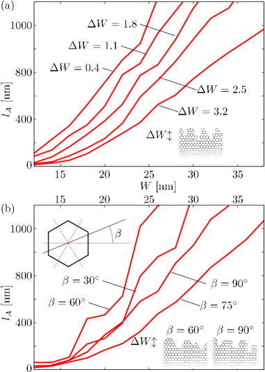
Qualitatively, we find the same Anderson localization behaviour [see figure 6(a)] as a function of ribbon width and roughness amplitude (for fixed ) as in the case with rectangular modules. However, unlike the case of free-particle dispersion Nikolic1994 , graphene nanostructures feature an interesting interplay between lattice orientation and surface roughness. As this interplay is determined by the alignment angle between the lattice orientation and the roughness, we can explicitly study its influence on transmission through the ribbon. We observe, indeed, that the value of the localization length strongly depends on the shape of the boundary with respect to the discrete lattice: edges consisting of randomly concatenated zigzag-edges only (i.e., with ) show substantially longer localization lengths than edges formed by an even mixture of zigzag and armchair edges [i.e., with ]. The dependence of the localization length on can be understood in terms of the length of undisturbed zigzag (or armchair) edges: cutting close to a symmetry plane of the lattice (i.e. or ) results in comparatively longer segments of zigzag (or armchair) edges. By contrast, a cut at yields an irregular sequence of very short segments of armchair and zigzag boundaries and thus strongly breaks the translation symmetry of a clean zigzag (or armchair) edge. As an aside we note that the data presented in the previous subsection includes a variation in ribbon direction, i.e., the ribbons are not perfectly straight, notably in figure 5(a, b). This amounts to an effective increase of edge roughness. As a result, the localization length is further decreased in that case [compare figure 5(d) with figure 6(b) for ].
The observation of the relative change in resistance as a function of , i.e., of the angle between the graphene lattice and the atomic-scale edge, might have implications for experiments. Measuring the atomic-scale roughness is difficult requiring an STM setup. Measuring localization length for different ribbon widths might provide an alternative probe for the atomic-scale edge roughness. Conversely, our results could be tested by comparing transport measurements for nanoribbons fabricated with different methods (i.e. etching, growth on Si-C substrates deHeer , unzipping of graphene nanotubes Crommie ) resulting in (known) different edge characteristics.
IV.4 Fourier analysis of channel states
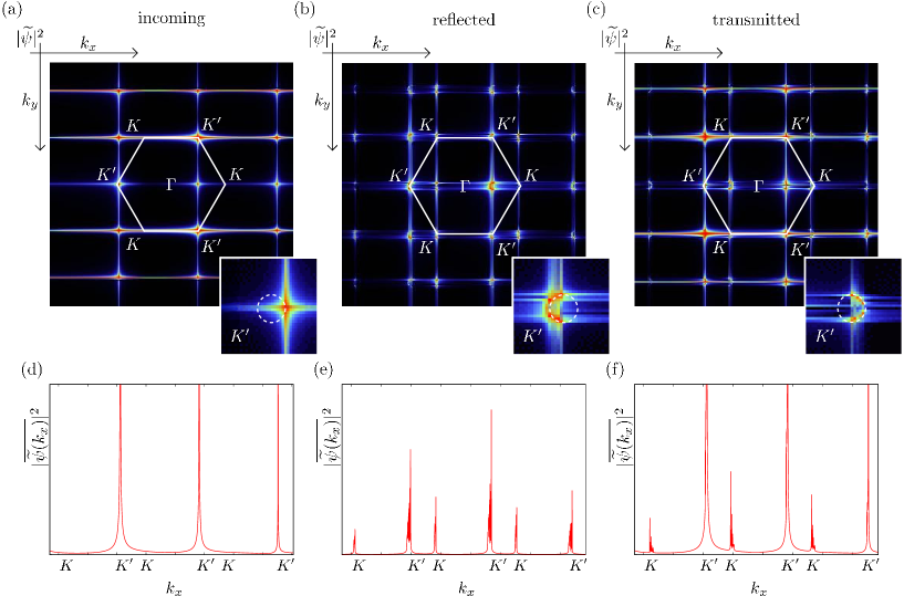
We explore now the interplay between short-range defects in real space and the absence (presence) of inter-cone scattering in -space. For this purpose we analyze the Fourier transforms of the asymptotic scattering state in the semi-infinite entrance (exit) waveguides. The Fourier transform is calculated as
| (20) |
where we extend the integral over a finite area in the asymptotic region of the waveguide, i.e., far away from the scattering region. Three different classes of asymptotic scattering states need to be considered: (i) the incoming Bloch states propagating in -direction with wavenumber ,
| (21) |
where represents the transverse eigenfunction of mode of the semi-infinite nanoribbon, (ii) the waves transmitted through the disordered region with transmission amplitude , and (iii) the reflected waves with reflection amplitude . The corresponding Fourier components are given by
| (22) | |||||
| (23) |
For a hexagonal lattice, the real and the reciprocal lattice are rotated by 90 degrees with respect to each other Ashcraft . The first Brillouin zone for the ideal zigzag ribbon is thus given by a hexagon resting on a side rather than on a tip [see white hexagon in figure 7(a)]. To better visualize the enhancement of near the or points, we integrate over the transverse direction,
| (24) |
In perfect zigzag ribbons, incoming modes feature non-vanishing amplitudes either near the or the point, i.e., there is no coupling (scattering) between and . For the incoming Bloch state the projected Fourier transform equation (24) features peaks at the values corresponding to [see figure 7(d)]. The close-up of the peak in near the point [inset of figure 7(a)] is structureless for the incoming Bloch wave with fixed transverse quantum number . The horizontal and vertical lines are finite-size effects of the Fourier-transformed sample. Likewise, the origin of the additional bright spots inside the Brillouin zone is zone folding (the Brillouin zone of the ribbon is smaller than the graphene Brillouin zone). The interesting physics, on the other hand, is contained in finite amplitudes at both and points of the scattered wave [see figure 7(b,c)] which are induced by scattering at rough edges. The relative strength of the integrated and peaks [see figure 7(e,f)] is a direct measure for the amount of inter-valley scattering. Furthermore, we observe a pronounced fine structure near the and points: enhancement along a half-circle forms around the Dirac points [see inset in figure 7(b,c)]. The surface of section of the double-cone band structure of constant energy is approximately a circle, the diameter of which is proportional to the energy. In the reflected (transmitted) part of the wavefunction, we only see the left half (right half) of this circle being populated, corresponding to negative (positive) group velocities. Enhancement along the full semicircle is due to inter-mode scattering between transverse modes within the same valley (intra-valley scattering). We can thus conclude that pronounced intra-valley scattering at the rough edges distributes the reflected (or transmitted) wave almost uniformly over the energetically accessible half-circle of the band structure compatible with their propagation direction. The Fourier transform thus allows us to assess the amount of both inter-valley scattering (by the relative amplitude around the and points in the reciprocal lattice) and inter-mode scattering by the angular distribution on the half-circle of a single cone for the incoming and reflected (or transmitted) states.
V Conclusions and Outlook
We have presented a novel numerical approach to efficiently calculate the Green’s function for extended nanoribbons. Key is the build-up of the ribbon by a random assembly of modules. Connecting these modules by way of a Dyson equation allows us to calculate the transport properties of long graphene ribbons. We find the conductance to be suppressed by rough edges relative to that of the perfect ribbon. For low energies, we observe near-perfectly conducting channels due to the band structure of zigzag graphene nanoribbons. Quantization steps are washed out and, in part, replaced by dips due to scattering into evanescent modes Ihnatsenka2 , in contrast to edge-disordered semiconductor nanoribbons with free-particle dispersion Nikolic1994 . An analysis of individual scattering states in both real space and Fourier space reveals pronounced sublattice asymmetries and scattering. We determined specific signatures of inter- and intra-valley scattering by Fourier transform spectroscopy of scattering states. We also identified Anderson localized states for different disorder configurations, extending over several micrometers with an exponential decay spanning 10 orders of magnitude. The corresponding localization length was calculated as a function of both the magnitude of edge roughness, and its alignment with the graphene lattice. We find that the latter plays a significant role in determining the localization length hinting at the importance of correctly modeling microscopic details of edge disorder beyond its amplitude and correlation length.
We conclude by pointing to possible future applications. While early transport measurements were strongly affected by substrate interactions resulting in puddles of electron and hole conductivity due to bulk disorder, recent advances in the manufacturing of much cleaner graphene nanostructures by growing on Si-C substrates deHeer , unzipping nanotubes to arrive at smooth-edged ribbons Crommie as well as suspended graphene vanWees have shifted the focus to edge disorder investigated in the present work. Indeed, the measurement of size quantization plateaus has been surprisingly elusive in graphene nanoribbons Molitor ; lin08 ; Kim2010 ; LewenkopfReview , in qualitative agreement with our present findings. Only recently, by prolonged annealing and suspending graphene nanoconstrictions, first signatures of size quantization could be found vanWees . Our findings regarding the sublattice sensitivity of the wavefunction (figure 3) could be tested by STM scans of bound states in graphene nano-islands Dinesh : in these measurements strong enhancements of wavefunction amplitudes were found on one sublattice, resulting in trigonal patterns close to edges that are quite similar to our numerical findings. Our simulations predict similar STM patterns for scattering states in extended nanostructures. In particular, such measurements could elucidate the precise nature of the scattering mechanisms encountered at edges prepared wth different techniques. Indeed, we expect defects affecting both sublattices, as recently investigated Ugeda , to exhibit different signatures than e.g. single vacancies. Finally, magnetic field effects allow for an additional external parameter more easily tunable in experiments than lattice geometries. States associated with different K points react differently to magnetic fields. This dependence might help to disentangle contributions from different -points in scattering accessible by our Fourier analysis. We note that our algorithm can be easily adapted to accomodate magnetic fields while retaining its favorable scaling properties. Investigations in this direction are currently under way.
Acknowledgements.
We thank K. Anson, L. Chizhova, J. Güttinger, and C. Stampfer for valuable discussions. Support by the Austrian Science Foundation (Grant No. FWF-P17359), the Max Kade Foundation and the SFB 041-ViCoM (FWF) is gratefully acknowledged. S.R. acknowledges support by the Vienna Science and Technology Fund (WWTF) through Project No. MA09-030 and by the Austrian Science Fund (FWF) through Project No. P14 in the SFB IR-ON. Numerical calculations were performed on the Vienna scientific cluster (VSC).References
References
- (1) K. S. Novoselov, E. McCann, V. M. S, V. I. Fal’ko, M. I. Katsnelson, U. Zeitler, D. Jiang, F. Schedin, and A. K. Geim, Nature Physics 2, 177 (2005a).
- (2) K. S. Novoselov, A. K. Geim, S. V. Morozov, D. Jiang, M. I. Katsnelson, I. V. Grigorieva, S. V. Dubonos, and A. A. Firsov, Nature 438, 197 (2005b).
- (3) K. S. Novoselov, A. K. Geim, S. V. Morozov, D. Jiang, M. Y. Zhang, S. V. Dubonos, I. V. Grigorieva, and A. A. Firsov, Science 306, 666 (2004).
- (4) A. H. C. Neto, F. Guinea, N. M. R. Peres, K. S. Novoselov, and A. K. Geim, Rev. Mod. Phys. 81, 109 (2009).
- (5) S. Das Sarma, S. Adam, E. H. Hwang and E. Rossi, Rev. Mod. Phys. 83, 407 (2011)
- (6) N. Dombay and A. Calogeracos, Phys. Rep. 315, 41 (1999).
- (7) M. I. Katsnelson, K. S. Novoselov, and A. K. Geim, Nat. Physics 2, 620 (2006).
- (8) C. Stampfer, J. Güttinger, F. Molitor, D. Graf, T. Ihn, and K. Ensslin, Appl. Phys. Lett. 92, 012102 (2008a).
- (9) C. Stampfer, E. Schurtenberger, F. Molitor, J. Güttinger, T. Ihn, and K. Ensslin, Nano Lett. 8, 2378 (2008b).
- (10) L. A. Ponomarenko, F. Schedin, M. I. Katsnelson, R. Yang, E. H. Hill, K. S. Novoselov, and A. K. Geim, Science 320, 356 (2008).
- (11) S. Schnez, F. Molitor, C. Stampfer, J. Güttinger, I. Shorubalko, T. Ihn, and K. Ensslin, Appl. Phys. Lett. 94, 012107 (2009).
- (12) J. Güttinger, C. Stampfer, S. Hellmüller, F. Molitor, T. Ihn, and K. Ensslin, Appl. Phys. Lett. 93 212102 (2008).
- (13) J. W. Klos and I. V. Zozoulenko, Phys. Rev. B 82, 081414(R) (2010).
- (14) A. MacKinnon, Z. Phys. B 59, 385 (1985).
- (15) D. K. Ferry and S. M. Goodwick, Transport in Nanostructures (Cambridge University Press, 1999).
- (16) H. U. Baranger, D. P. DiVincenzo, R. A. Jalabert, and A. D. Stone, Phys. Rev. B 44, 10637 (1991).
- (17) E. R. Mucciolo, A. H. Castro-Neto, and C. H. Lewenkopf, Phys. Rev. B 79, 075407 (2009).
- (18) A. Cresti, and S. Roche, Phys. Rev. B 79, 233404 (1989).
- (19) M. Evaldsson, I. V. Zozoulenko, H. Xu, and T. Heinzel Phys. Rev. B 78, 161407(R) (2008).
- (20) B. Trauzettel, D. V. Bulaev, D. Loss, and G. Burkard, Nat. Physics 3, 192 (2007).
- (21) A. Cresti, R. Farchioni, G. Grosso, and G. P. Parravicini, Phys. Rev. B 68, 075306 (2003).
- (22) G. Metalidis and P. Bruno, Phys. Rev. B 72, 235304 (2005).
- (23) N. Neophytou, S. Ahmed, and G. Klimeck, J. Comput. Electron.6, 317 (2007).
- (24) A. Svizhenko, M. P. Anantram, T. R. Govindan, and B. Biegel, J.Appl. Phys. 91, 2343 (2002).
- (25) F. Sols, M. Macucci, U. Ravaioli, and K. Hess, J. Appl. Phys. 66, 3892 (1989).
- (26) S. Rotter, J.-Z. Tang, L. Wirtz, J. Trost, and J. Burgdörfer, Phys. Rev. B 62, 1950 (2000).
- (27) S. Rotter, B. Weingartner, N. Rohringer, and J. Burgdörfer, Phys. Rev. B 68, 165302 (2003).
- (28) K. Kazymyrenko and X. Waintal, Phys. Rev. B 77, 115119 (2008).
- (29) M. Wimmer and K. Richter, J. Comp. Phys. 228, 8548 (2009).
- (30) P. S. Drouvelis, P. Schmelcher, and P. Bastian, J. Comp. Phys. 215, 741 (2006).
- (31) D. Mamaluy, D. Vasileska, M. Sabathil, T. Zibold, and P. Vogl, Phys. Rev. B 71, 245321 (2005).
- (32) J. Feist, A. Bäcker, R. Ketzmerick, S. Rotter, B. Huckestein, and J. Burgdörfer, Phys. Rev. Lett. 97, 116804 (2006).
- (33) J. Feist, A. Bäcker, R. Ketzmerick, J. Burgdörfer, and S. Rotter, Phys. Rev. B 80, 245322 (2009).
- (34) P. R. Wallace, Phys. Rev. 71, 622 (1947).
- (35) S. Reich, J. Maultzsch, C. Thomsen, and P. Ordejón, Phys. Rev. B 66, 035412 (2002).
- (36) A. Grüneis, C. Attaccalite, L. Wirtz, H. Shiozawa, R. Saito, T. Pichler, and A. Rubio, Phys. Rev. B 78, 205425 (2008).
- (37) F. Libisch, C. Stampfer, and J. Burgdörfer, Phys. Rev. B 79, 115423 (2009).
- (38) E. McCann, K. Kechedzhi, V. I. Fal’ko, H. Suzuura, T. Ando, and B. L. Altshuler, Phys. Rev. Lett 97, 146805 (2006).
- (39) G. W. Semenoff, Phys. Rev. Lett. 53, 2449 (1984).
- (40) M. M. Ugeda, I. Brihuega, F. Hiebel, P. Mallet, J-Y. Veuillen, J. M. Gómez-Rodriguez, and F. Ynduráin, Phys. Rev. B 85, 121402(R) (2012).
- (41) S. Rotter, B. Weingartner, F. Libisch, F. Aigner, J. Feist, and J. Burgdörfer, Lect. N. Comp. Science 3743, 586 (2006).
- (42) S. Sanvito, C. J. Lambert, J. H. Jefferson, and A. M. Bratkovsky, Phys. Rev. B 59, 11936 (1999).
- (43) P. R. Amestoy, I. S. Duff, J. Koster, and J.-Y. L’Excellent, SIAM Journal of Matrix Analysis and Applications 23, 15-41 (2001); P. R. Amestoy, A. Guermouche, J.-Y. L’Excellent and S. Pralet, Parallel Computing 32, 136-156 (2006).
- (44) C. Berger et al., Science 312, 1191 (2006)
- (45) Y. Zhang, Y.-W. Tan, H. L. Stormer, and P. Kim, Nature 438, 201 (2005).
- (46) Y. Niimi, T. Matsui, H. Kambara, K. Tagami, M. Tsukada, and H. Fukuyama, Phys. Rev. B 73, 085421 (2006).
- (47) S. Ihnatsenka and G. Kirczenow, Phys. Rev. B 80, 201407R (2009).
- (48) S. Ihnatsenka and G. Kirczenow, Phys. Rev. B 85, 121407(R) (2012)
- (49) K. Nikolić and A. MacKinnon, Phys. Rev. B 50, 11008 (1994).
- (50) P. F. Bagwell, Phys. Rev. B 41, 10354 (1990).
- (51) F. Libisch, S. Rotter, and J. Burgdörfer, Phys. Stat. Sol. B 248, 2598 (2011).
- (52) K. Wakabayashi, Y. Takane, M. Yamamoto, and M. Sigrist CARBON(Elsevier) 47, 124 (2009).
- (53) S-J. Xiong and Y. Xiong, Phys. Rev. B 76, 214204 (2007)
- (54) X. Li, X. Wang, L. Zhang, S. Lee, and H. Dai, Science 319, 1229 (2008); C. Tao et al., Nature Physics 7, 616 (2011).
- (55) D. Subramaniam et al., Phys. Rev. Lett. 108, 046801 (2012); S. H. Park et al., ACS Nano 5, 8162 (2011); S. K. Hämäläinen et al., Phys. Rev. Lett. 107, 236803 (2011).
- (56) N. W. Ashcroft and N. D. Mermin, Solid State Physics (Thomson Learning Inc., Cornell, 1976).
- (57) N. Tombros, A. Veligura, J. Junesch, M. H. D. Guimaraes, I. J. V. Marun, H. T. Jonkman, and B. J. van Wees Nature Physics 7, 697 (2011),
- (58) F. Molitor, A. Jacobsen, C. Stampfer, J. Güttinger, T. Ihn, and K. Ensslin, Phys. Rev. B 79, 075426 (2009).
- (59) Y.-M. Lin, V. Perebeinos, Z. Chen, and P. Avouris, Phys. Rev. B 78, 161409 (2008).
- (60) M. Y. Han, J. C. Brant, and P. Kim, Phys. Rev. Lett. 104, 056801 (2010).
- (61) E. R. Mucciolo and C. H. Lewenkopf, J. Phys. Cond. Matt 22, 273201 (2010).