Charge control in laterally coupled double quantum dots
Abstract
We investigate the electronic and optical properties of InAs double quantum dots grown on GaAs (001) and laterally aligned along the [110] crystal direction. The emission spectrum has been investigated as a function of a lateral electric field applied along the quantum dot pair mutual axis. The number of confined electrons can be controlled with the external bias leading to sharp energy shifts which we use to identify the emission from neutral and charged exciton complexes. Quantum tunnelling of these electrons is proposed to explain the reversed ordering of the trion emission lines as compared to that of excitons in our system.
Optical spin initialization of individual electrons is a fundamental resource for quantum information science which relies on our ability to control the charge in a quantum dot (QD) molecule. Robledo et al. (2008); Kim et al. (2008, 2011) In the last years, vertically aligned QDs have been fabricated with great success. In these systems, exciton coupling signatures including energy anticrossings of neutral and charged exciton complexes have been demonstrated by applying an electric field in the growth direction. Krenner et al. (2005); Stinaff et al. (2006); Scheibner et al. (2007) Lateral QD molecules would be a better candidate for scaling-up the electronic coupling from two to several QDs applying individual lateral gates. Previous demonstrations of electronic coupling in a lateral QD pair have been based on analysis of the anomalous Stark shifts and photon correlation statistics of the neutral exciton under a lateral electric field. Beirne et al. (2006) Yet, the observation of electrically tunable energy anticrossings in lateral QD molecules remains a difficult task due the exponential decrease of the tunnel coupling energy with the center to center QD distance, . Beirne et al. (2006); Wang et al. (2009); Peng and Bester (2010) In the following, we investigate the emission spectrum of electrically tunable lateral QD pairs with varying number of electrons. For typical inter-dot distances nm, we find that electron tunnelling phenomena affect the negative trion emission energy before clear exciton anticrossings may take place.
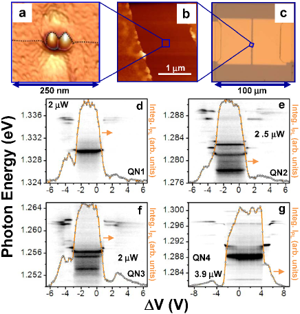
For the present study, QD pairs aligned in the [110] crystal direction were fabricated on GaAs nanoholes using a modified droplet epitaxy growth procedure as described in detail elsewhere. Alonso-Gonzalez et al. (2009) The nanostructures were grown on a 0.5-m-thick undoped GaAs buffer layer and capped by 100 nm of undoped GaAs. Atomic force micrographs (AFM) performed on a similar uncapped sample revealed that each QD in the pair has slightly different height, with average values of nm and nm, respectively, and center to center separation equal to their average diameter nm [Fig. 1(a)]. The morphological analysis also revealed that QD pair formation occurs in 95 % of the cases with a small probability for single QDs or empty nanoholes. The low areal density of cm-2 is adequate to study individual quantum nanostructures.
To apply an electric field along the QD pair mutual axis, we defined metal-semiconductor-metal (MSM) diodes by evaporation of two metal contacts (15 nm Mo + 30 nm Au) on top of a 100 m square mesas. The contacts are separated by a 80 m long1.5 m wide undoped GaAs channel embedding the nanostructures as shown in Figures 1(a-c). The micro-photoluminescence (-PL) of individual QD pairs was collected at 5 K using a fiber based confocal microscope, excited with 785 nm continuous wave laser light, dispersed by a 20.3 m focal length double spectrograph and detected with a peltier cooled Silicon CCD camera. The spectral resolution of our setup is 90 eV full width at half maximum (FWHM).
In the last few years, several groups have investigated the emission of single semiconductor nanostructures in the presence of a lateral electric field. For moderate electric fields, or when the separation between the contacts is large, the changes observed in the QD spectrum have been related to the modulation of the carrier capture probability induced by the external field. Moskalenko et al. (2006, 2007) The capture mechanisms also play the most important role in single QDs dynamically driven by surface acoustic waves. Volk et al. (2010, 2011) The laterally applied bias can also modulate the electronic confinement levels. This requires of larger electric fields or smaller contact separation for a given bias range. In this regime, the exciton wavefunction can be directly modified leading to energy shifts, carrier tunnelling and fine structure splitting reduction among other effects. Kowalik et al. (2005); Stavarache et al. (2006); Gerardot et al. (2007); Reimer et al. (2008); Alén et al. (2009) With a channel width of only 1.5 m, our MSM diodes have been designed to apply large electric fields in the [110] crystal direction (0-60 kV/cm). This is required to tune independently the exciton energy of the two QDs in a lateral molecule and, if their separation were small enough, to observe resonant quantum tunnelling phenomena.
The contour maps in fig. 1 (d-f) show the evolution of the -PL spectrum as a function of the lateral bias, , for four different nanostructures (QN1-QN4). In each case, the evolution of the spectrally integrated intensity is also drawn [orange (spotted) lines]. The integrated intensity remains constant within 10% for a broad voltage range around a certain bias V and diminishes down to zero for larger positive or negative bias. While the intensity decreases, the emission spectrum also changes giving rise to blue-shifted spectral features which are different in each nanostructure as shown in the -PL contour maps. These emission patterns can be examined to distinguish between single quantum dots (QN1) and double quantum dots (QN2-QN4) as exemplarily explained below for QN1 and QN2.
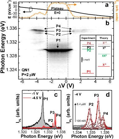
To do so, we have analyzed the device operation using semi-analytical transport equations valid for one-dimensional (1D) MSM structures. end The simulations are performed in dark conditions and explain why the spectrum is not fully symmetric around 0 V. Attending to the particular position of the nanostructure within the GaAs channel, the electric field is calculated neglecting possible screening effects induced by the photogenerated carriers. Figure 2(a) show the dependence [black line] at the position of QN1 which we estimate according to the model at 530 nm from the left contact. The curve shows a plateau which extends over the bias region where the field is still zero at this position. In this region, the integrated intensity [orange (spotted) line] and the -PL spectrum [contour plot map in fig. 2(b)] is independent of the voltage and, in the case of QN1, is characterized by a single broad resonance at 1.330 eV (labelled as P1). As we approach to the edges of the plateau raising , the electric field in the vicinity of the nanostructure also increases. In such situation, the possibility of an enhanced capture of carriers driven by the external lateral field was discussed by Moskalenko et al. Moskalenko et al. (2007) They found that the overall QD integrated intensity increased rather than decreased for both positive and negative bias and also reported switching between spectral lines. The later was explained by the uneven capture of electron and holes and was found strongly dependent on the excitation energy and power and also on the temperature. In our case, we observe an overall reduction of the integrated intensity and switching between spectral lines which are similar in a wide range of excitation powers and temperatures. end Our observations should be thus related to the large electric fields present in our devices and to intrinsic properties of InAs quantum dots and quantum dot pairs grown by modified droplet epitaxy.
The decrease of the integrated intensity at both sides of the central plateau might be explained through the combination of two effects. First, electron and holes photogenerated above barrier can drift away from the illuminated area, before being captured in the quantum dots, contributing to the subnanosecond photocurrent response of MSM photodetectors of this size. Wei et al. (1981) Secondly, carriers already confined in the nanostructure can tunnel out due to the large applied field. The later causes the switching of spectral lines which we associate to the recombination of exciton complexes with varying number of electrons. Alén et al. (2005) If the crystallization of the Ga droplet is not complete, arsenic vacancies arise during growth creating localized states in the gap. These localized states are close in energy to the electron confined levels and are occupied by one or more electrons depending on their state of valence. Laasonen et al. (1992) Thus, in absence of an electric field, the negatively charged environment leads to a luminescence spectrum dominated by negatively charged exciton complexes. Alonso-González et al. (2007) When a bias is applied in either direction, these electrons are swept by the electric field leading to neutral or positively charged exciton recombination.
Together with the external field, the local field associated to ionized defects Kamada and Kutsuwa (2008); Moskalenko et al. (2007) and the screening field created by the accumulation of photogenerated carriers in the metal-semiconductor interfaces Wei et al. (1981) must be considered. The local field fluctuates due to the dynamics of the charged environment. Kamada and Kutsuwa (2008) This broadens the emission lines by spectral diffusion, as shown in Figure 2(c) for the spectral line P1 (FWHM800 eV). The fluctuations are largely minimized once the extra charges have been swept and switching to spectral lines P2-P4 (FWHM110-260 eV) takes place. Meanwhile, the screening is likely the responsible of small energy shifts which we observe when varying the excitation power at constant bias [Fig. 2(c)]. Both effects are small, typically 100-500 eV, and can be disregarded for the analysis of the charge tuning effect where large shifts (1-8 meV), associated to carrier-carrier interactions, are induced by the external bias. Both effects can be also minimized by using a resonant excitation scheme. Moskalenko et al. (2007)
The charge tunability is crucial for applications in quantum information technology and also to identify the different spectral lines in our experiment. The tunnelling rates are determined by the carrier confinement energies and therefore depend on the QD size and the Coulomb interactions between electrons and holes. Warburton et al. (2000); Alén et al. (2005) This leads to -PL contour maps with characteristic stair-case patterns and energy splittings which are different for single QDs and QD pairs.
The four spectral lines (P1-P4) in the spectrum of Fig. 2(b) can be well described assuming that QN1 is a single QD. To do so, the electronic structure has been calculated using a 2D effective mass model for electrons and heavy holes. end We calculate the emission energy of the neutral exciton (X0), negative and positive trions (X-, X+), biexciton (XX0) and negative quarton (X2-) [Inset of Fig. 2(b)]. By comparing the energetic ordering with that of the experiment, we find that lines P1,P2,P3 and P4 correlate well with X-, XX0, X0 and X+ optical transitions, respectively. The X2- triplet resonance, which would show up at lower energies, is not observed in the spectrum indicating that only one electron is being transferred from the environment to this particular QD.
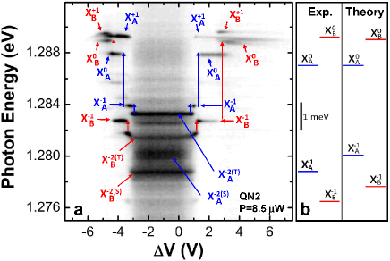
AFM performed in uncapped samples reveals that most of the nanoholes contain lateral QD pairs. Accordingly, most of our spectra can not be described assuming just a single QD. In Figure 3, we analyze in detail the spectrum of QN2 which is characterized by twice the number of spectral lines expected for a single QD. Beirne et al. (2006); Pomraenke et al. (2008); Abbarchi et al. (2009); Wang et al. (2009) The spectrum of QN2 can be understood by the tentative assignment proposed in the figure, which is roughly that of two single QDs, A and B, with emission from X2-, , and . The two QDs are asymmetric, as usually observed in AFM, with A being slightly bigger. Starting from the X2- transitions (singlet and triplet), with increasing external field, the number of additional electrons is tuned from two to zero and each QD in the pair follows its own Coulomb staircase: X2- X- X0 X+. This shows that net confined charge can be controlled in a QD pair by applying a lateral electric field.
The energy ordering in the spectral assignment of Fig. 3 is the usual one for isolated QDs. Yet, there is a remarkable anomaly. The emission energy of X is lower than that of X, indicating that QD A is bigger than QD B. However, the emission energy of X is higher than that of X. This result is difficult to explain in terms of isolated QDs. If we assume that the different structural conditions of the QDs lead to lower energy for X, they should also lead to lower energy for X.Climente et al. (2008) The anomalous behavior can be explained if the electrons in the QD pair are tunnel coupled. To illustrate this point, in Fig. 3(b) we compare the experimental energies of neutral and negatively charged excitons (left column) with those of a coupled QD pair (right column). The QDs have the same parameters as in the single QD case of Fig. 2, but QD A is now slightly bigger ( meV). To enable tunnel coupling, we consider the distance between the centers of the QDs is nm, which is slightly below the average value found by AFM. Under these conditions, not only the calculated energy ordering is the same as in the experiment, but also we obtain remarkable agreement in the energy splittings. In the experiment, the X0 peaks are split by meV and the X- peaks by meV. In the calculations, the corresponding values are meV and meV, respectively.
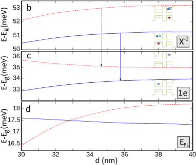
To understand the reversed ordering of the trion emission lines as compared to that of excitons, one must notice the different response of the two species when the QD pair is approached. In asymmetric QD pairs, the energy splitting between the two direct X0 states (X and X) is barely sensitive to the interdot distance, up to very small separations.Baira et al. (2008) The situation is similar for X-, as shown in Fig. 4(a). However, the final electron states display a pronounced tunnel coupling,Peng et al. (2010) which translates into a sizable energy splitting with decreasing interdot distance, see Fig. 4(b). In particular, the electron in QD B evolves towards an antibonding molecular state. As a consequence, the emission energy () of the trion in QD B decreases and eventually crosses that of QD A at nm, as shown in Fig. 4(c). A further reduction in the interdot distance results in the reversed ordering of our experimental spectra.
To conclude, we have shown how the number of electrons can be electrically controlled in lateral QD pairs embedded in a lateral Schottky diode. As the number of confined electrons is lowered, carrier-carrier interactions give rise to well defined energy shifts which we compare with a theoretical model including Coulomb interactions and electron tunnel coupling. We have found that the negative trion emission energy is sensitive to single electron tunneling for interdot distances nm. These results are relevant in the field of scalable quantum information processing using laterally coupled QDs.
The authors wish to acknowledge to Spanish MICINN through projects Consolider-Ingenio 2010 QOIT (CSD2006-0019), TEC2008-06756-C03-01/03 and CTQ2008-03344, and to Comunidad Autónoma de Madrid through project Q&CLight (S2009ESP-1503).
References
- Robledo et al. (2008) L. Robledo, J. Elzerman, G. Jundt, M. Atatüre, A. Högele, S. Fält, and A. Imamoglu, Science 320, 772 (2008).
- Kim et al. (2008) D. Kim, S. E. Economou, S. C. Badescu, M. Scheibner, A. S. Bracker, M. Bashkansky, T. L. Reinecke, and D. Gammon, Phys. Rev. Lett. 101, 236804 (2008).
- Kim et al. (2011) D. Kim, S. G. Carter, A. Greilich, A. S. Bracker, and D. Gammon, Nat Phys 7, 223 (2011).
- Krenner et al. (2005) H. J. Krenner, M. Sabathil, E. C. Clark, A. Kress, D. Schuh, M. Bichler, G. Abstreiter, and J. J. Finley, Phys. Rev. Lett. 94, 057402 (2005).
- Stinaff et al. (2006) E. A. Stinaff, M. Scheibner, A. S. Bracker, I. V. Ponomarev, V. L. Korenev, M. E. Ware, M. F. Doty, T. L. Reinecke, and D. Gammon, Science 311, 636 (2006).
- Scheibner et al. (2007) M. Scheibner, I. V. Ponomarev, E. A. Stinaff, M. F. Doty, A. S. Bracker, C. S. Hellberg, T. L. Reinecke, and D. Gammon, Phys. Rev. Lett. 99, 197402 (2007).
- Beirne et al. (2006) G. J. Beirne, C. Hermannstädter, L. Wang, A. Rastelli, O. G. Schmidt, and P. Michler, Phys. Rev. Lett. 96, 137401 (2006).
- Wang et al. (2009) L. Wang, A. Rastelli, S. Kiravittaya, M. Benyoucef, and O. G. Schmidt, Adv. Mat. 21, 2601 (2009).
- Peng and Bester (2010) J. Peng and G. Bester, Phys. Rev. B 82, 235314 (2010).
- Alonso-Gonzalez et al. (2009) P. Alonso-Gonzalez, J. Martin-Sanchez, Y. Gonzalez, B. Alen, D. Fuster, and L. Gonzalez, Crystal Growth & Design 9, 2525 (2009).
- Moskalenko et al. (2006) E. S. Moskalenko, M. Larsson, W. V. Schoenfeld, P. M. Petroff, and P. O. Holtz, Phys. Rev. B 73, 155336 (2006).
- Moskalenko et al. (2007) E. S. Moskalenko, M. Larsson, K. F. Karlsson, P. O. Holtz, B. Monemar, W. V. Schoenfeld, and P. M. Petroff, Nano Letters 7, 188 (2007).
- Volk et al. (2010) S. Volk, F. J. R. Schulein, F. Knall, D. Reuter, A. D. Wieck, T. A. Truong, H. Kim, P. M. Petroff, A. Wixforth, and H. J. Krenner, Nano Letters 10, 3399 (2010).
- Volk et al. (2011) S. Volk, F. Knall, F. J. R. Schulein, T. A. Truong, H. Kim, P. M. Petroff, A. Wixforth, and H. J. Krenner, Appl. Phys. Lett. 98, 023109 (2011).
- Kowalik et al. (2005) K. Kowalik, O. Krebs, A. Lemaı^tre, S. Laurent, P. Senellart, P. Voisin, and J. A. Gaj, Appl. Phys. Lett. 86, 041907 (2005).
- Stavarache et al. (2006) V. Stavarache, D. Reuter, A. D. Wieck, M. Schwab, D. R. Yakovlev, R. Oulton, and M. Bayer, Appl. Phys. Lett. 89, 123105 (2006).
- Gerardot et al. (2007) B. D. Gerardot, S. Seidl, P. A. Dalgarno, R. J. Warburton, D. Granados, J. M. Garcia, K. Kowalik, O. Krebs, K. Karrai, A. Badolato, et al., Appl. Phys. Lett. 90, 041101 (2007).
- Reimer et al. (2008) M. E. Reimer, W. R. McKinnon, J. Lapointe, D. Dalacu, P. Poole, G. C. Aers, D. Kim, M. Korkusinski, P. Hawrylak, and R. L. Williams, Physica E 40, 1790 (2008).
- Alén et al. (2009) B. Alén, D. Fuster, I. Fernández-Martínez, J. Martínez-Pastor, Y. González, F. Briones, and L. González, Nanotechnology 20, 475202 (2009).
- (20) See supplementary information file for an explanation of the theoretical models and evolution of spectral switching with power and temperature.
- Wei et al. (1981) C. Wei, H. Klein, and H. Beneking, Electronics Letters 17, 688 (1981).
- Alén et al. (2005) B. Alén, J. Martínez-Pastor, D. Granados, and J. M. García, Phys. Rev. B 72, 155331 (2005).
- Laasonen et al. (1992) K. Laasonen, R. M. Nieminen, and M. J. Puska, Phys. Rev.B 45, 4122 (1992).
- Alonso-González et al. (2007) P. Alonso-González, B. Alén, D. Fuster, Y. González, and L. González, Appl. Phys. Lett. 91, 163104 (2007).
- Kamada and Kutsuwa (2008) H. Kamada and T. Kutsuwa, Phys. Rev. B 78, 155324 (2008).
- Warburton et al. (2000) R. J. Warburton, C. Schäflein, D. Haft, F. Bickel, A. Lorke, K. Karrai, J. M. García, W. Schoenfeld, and P. M. Petroff, Nature 405, 926 (2000).
- Pomraenke et al. (2008) R. Pomraenke, C. Lienau, Y. I. Mazur, Z. M. Wang, B. Liang, G. G. Tarasov, and G. J. Salamo, Phys. Rev. B 77, 075314 (2008).
- Abbarchi et al. (2009) M. Abbarchi, C. A. Mastrandrea, A. Vinattieri, S. Sanguinetti, T. Mano, T. Kuroda, N. Koguchi, K. Sakoda, and M. Gurioli, Phys. Rev. B 79, 085308 (2009).
- Climente et al. (2008) J. I. Climente, A. Bertoni, and G. Goldoni, Phys. Rev. B 78, 155316 (2008).
- Baira et al. (2008) M. Baira, L. Sfaxi, L. Bouzaiene, H. Maaref, N. Chauvin, and C. Bru-Chevallier, J. Appl. Phys. 104, 064314 (2008).
- Peng et al. (2010) J. Peng, C. Hermannstädter, M. Witzany, M. Heldmaier, L. Wang, S. Kiravittaya, A. Rastelli, O. G. Schmidt, P. Michler, and G. Bester, Phys. Rev. B 81, 205315 (2010).
Figure Captions
Figure 1.- (Color online) a), b) and c) show two AFM images and an optical image of a single QD pair, a 1.5-m-wide GaAs channel, and a full MSM device, respectively. d) to f) show contour maps of the bias dependent -PL measured in four different nanostructures. The orange (spotted) lines stand for the -PL intensity integrated in the corresponding emission ranges.
Figure 2.- (Color online) a) Electric field vs. bias dependence calculated using a semi-analytical transport model [black line]. Spectrally integrated -PL intensity obtained in the same bias range [orange (spotted) line]. b) -PL contour plot map vs. lateral bias measured for QN1. The inset compares the experimental [left] and theoretical [right] emission energies for lines P1-P4. c) Two spectra extracted from the contour plot at the indicated voltages. d) Excitation power evolution of P1-P4 and corresponding lorentzian fits (solid lines].
Figure 3.- (Color online) a) -PL contour plot map vs. lateral bias measured for QN2. b) Comparison between experimental [left] and theoretical [right] energies for X0 and X- emission from QD A and B ( nm).
Figure 4.- (Color online) Calculated energy of the negative trions (a), electrons (b) and corresponding trion emission line (c) as a function of the interdot distance, . The insets indicate the location of electrons and holes in the long limit. is the gap energy.