Nonlinear interaction of spin and charge currents in graphene
Abstract
We describe a nonlinear interaction between charge currents and spin currents which arises from the energy dependence of the conductivity. This allows nonmagnetic contacts to be used for measuring and controlling spin signals. We choose graphene as a model system to study these effects and predict its magnitudes in nonlocal spin valve devices. The ambipolar behavior of graphene is used to demonstrate amplification of spin accumulation in p-n junctions by applying a charge current through nonmagnetic contacts.
pacs:
72.25.Hg, 72.80.Vp, 75.76.+j, 85.75.-dSpin-polarized transport (spintronics) Žutić et al. (2004) in graphene, a one-atom-thick layer of carbon Castro-Neto et al. (2009), is of both fundamental and technological interest due to its long spin relaxation length Tombros et al. (2007) and large spin signals Han et al. (2010). In this work we focus on understanding graphene spintronics as it is experimentally addressed by an all-electrical scheme involving the use of a nonlocal device geometry Tombros et al. (2007). The conductivity in graphene has been considered only at the Fermi level, which leads to equal values for both spin channels. We point out that very recent work Abanin et al. (2011) uses the energy dependent conductivity of graphene, in conjunction with Zeeman splitting by applied magnetic fields, to explain a giant spin-Hall effect in the linear regime.
In this contribution we highlight nonlinear effects in the absence of external magnetic field that gives rise to interactions between electron spin and charge in graphene. We argue that the nonlinear interaction between spin and charge can be consistently described by using the equations for spin diffusion in metals van Son et al. (1987); Valet and Fert (1993), while considering the energy dependent conductivity of graphene and the large spin accumulation achievable by spin injection. This gives rise to phenomena observable in the nonlocal geometry, which include detection of spin accumulation in graphene via nonmagnetic contacts, its manipulation using charge currents and amplification in bipolar devices.
Previous experimental work has shown the manipulation of spin accumulation in graphene by applying high electric fields Józsa et al. (2008); *jozsa_controlling_2009. Such a manipulation has been later interpreted by considering the effect of low-resistance contacts Yu et al. (2010) within the drift-diffusion formalism for spin accumulation derived for semiconductors Yu and Flatté (2002a); *yu_spin_2002. In the following, we consider highly resistive noninvasive contacts Schmidt et al. (2000); Rashba (2000), which can be treated as ideal (spin) current injectors and (spin) voltage detectors Popinciuc et al. (2009); Han et al. (2010). This allows us to only focus on the physics of spin transport within graphene.
We start with the well established model for spin transport in metals van Son et al. (1987); Valet and Fert (1993) with the electrochemical potential for each spin channel expressed as , where the index refers to electron spin . Here, is the term related to the spin accumulation and the average potential. This results in spin-diffusion equations
| (1) | |||||
| (2) |
with the electron charge, the spin relaxation length, and the conductivities and the currents for each spin channel, and . As shown in Eq. (2), the gradient in drives the current for each spin channel in opposite directions, whereas the electric field drives them in the same direction. The spin-dependent conductivities are described by the polarization such that . The general solutions for , , and in a homogeneous medium were presented in Appendix C of Ref. Valet and Fert, 1993. To find numerical solutions for a certain device configuration we divide the graphene into discrete regions and use the solutions for each region, while keeping continuities of and .
In metals it is possible to achieve a spin accumulation eV Jedema et al. (2002) whereas in graphene it can be considerably larger, as explained below. Electrical spin injection from a tunnel contact with polarization using a charge current results in injection of a spin current . Ignoring any interaction between spin and charge, decays away from the injector as given by Tombros et al. (2007)
| (3) |
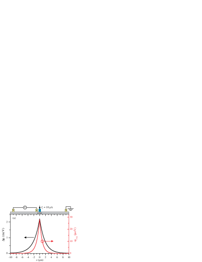
with the graphene square resistance, its width, and the nonlocal spin resistance as measured by a second magnetic contact with same . For typical values of k, m, m, A and % the resulting profile reaches meV, as depicted in Fig. 1(a). At such large splitting in the electrochemical potential the energy dependence of the graphene conductivity starts to be noticeable. Therefore we introduce a splitting dependent given by
| (4) |
with a conductivity spin polarization proportional to and a coefficient . The effects of temperature and disorder, described later, can be taken into account by considering the experimental electrical conductivity .
Now, we discuss the nature of the coefficient . The conductivity of graphene away from the neutrality (Dirac) point can be described by , with the carrier mobility and the carrier density. Due to the linear density of states in graphene Castro-Neto et al. (2009) the carrier density depends on energy as , where is the reduced Planck constant and m/s is the Fermi velocity. For a constant mobility, the latter leads to , so diverges when tends to zero. Therefore the maximum value of is given by the mechanisms limiting how close we can get to . The charge carrier density in graphene field-effect transistors is electrostatically tunable by applying a voltage to a gate such that with the gate capacitance per unit area and the voltage at which the neutrality point is located. A background carrier density is induced by the presence of electron-hole puddles () due to disorder Martin et al. (2008) and thermal generation of carriers () Dorgan et al. (2010). Up to date, all spintronic devices have been fabricated with graphene supported on a substrate, mostly SiO2. At room temperature, for a typical value of cm-2, we obtain a maximum value of meV)-1 which together with meV yields %.
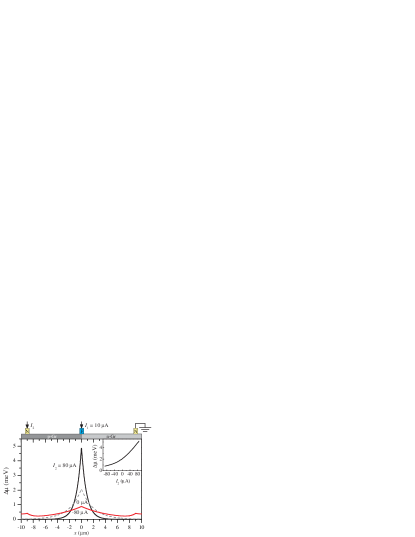
We use the modeling above to study spin transport in graphene field-effect transistors. We can describe most experimental vs (Dirac) curves for graphene on SiO2 by taking a constant value of m2/Vs and a carrier density Dorgan et al. (2010). For simplicity, we keep the polarization of magnetic contacts fixed at % and a carrier density independent spin relaxation length of m. Unless stated otherwise, we use cm-2 [ meV)-1], well into the metallic regime. First, we consider in Fig. 1(a) a nonlocal measurement where a spin current is injected into graphene. The presence of a spin current in graphene with an inhomogeneous conductivity polarization creates a nonlocal charge voltage . Interestingly, such a potential is detectable with both magnetic and nonmagnetic contacts. For the simple case of pure spin current injection (ignoring the effect of the charge current on the right side of the circuit) we obtain
| (5) |
which indicates that this is a second order effect in . The latter also means that must decay with a characteristic length of . The nonlinear nature of is explicit in the inset of Fig. 1(b). This effect opens the unique possibility of measuring spin signals in graphene without using magnetic detectors.
Next, we consider the effect of changing the graphene carrier density on . We calculate from Eq. (4) using the simulated electrical conductivity , which includes the effect of , such that . The coefficient has opposite polarity for hole and electron regimes. Besides, a finite introduces the presence of both electrons and holes near the Dirac point, which removes the divergence of and makes it zero. This behavior is in analogy to the case of the thermoelectric Seebeck coefficient which has the same dependence on as and follows an approximate Mott formula based on the experimental Dirac curve Löfwander and Fogelström (2007); *zuev_thermoelectric_2009. From Eqs. (3), (4) and (5) the dependence of on energy is given by .
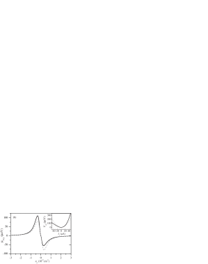
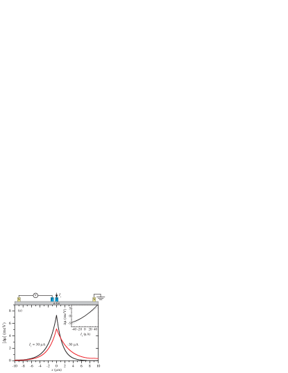
The nonlocal charge voltage goes as for injection of pure spin currents. If we also consider the charge current on the right side of the circuit [Fig. 1(a)], an asymmetry in the vs curve is visible [inset in Fig. 1(b)]. This is a higher () order effect on given by the interaction of with the spin accumulation on the right side of the circuit, which creates a higher () order effect on the nonlocal spin accumulation . We make explicit such an effect on in Fig. 2(a). The resulting nonlocal spin resistance detected in a spin valve with a second magnetic contact, , now varies with the injection current, as observed in the nonlinear behavior shown in the inset of Fig. 2(a).
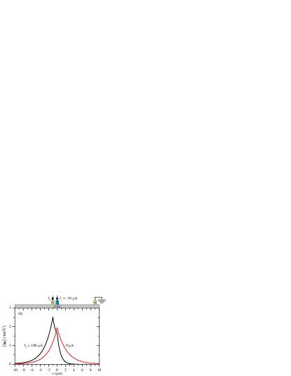
An interesting result is observed if we consider a second charge current via a nonmagnetic contact, as depicted in Fig. 2(b). A spin accumulation in graphene creates a conductivity spin polarization , which in the presence of a charge current gives rise to a spin current . The nonmagnetic contact hence seems to inject a spin current similarly to the case of a magnetic contact. Depending on the polarities of and , spin accumulation or depletion is observed. The nonmagnetic contact offers an extra handle by which we can amplify the spin accumulation. As shown in Fig. 2(b), under the nonmagnetic contact can be even larger than that under the magnetic contact.
In graphene field-effect devices we can individually address specific regions via local electrostatic gates. We use this capability to study ambipolar spin transport in graphene. We choose a highly symmetric case where the physics can be easily understood and derive a simple analytical description which accurately describe the simulations. The latter is possible because in graphene we can ignore the effects of the charge depletion region present in nondegenerate p-n junctions Žutić et al. (2004); Pershin and Privman (2003).
We consider a graphene channel with the left half set in the hole regime and the right half set in the electron regime, as depicted in Fig. 3. Initially, with , the magnetic contact located at the junction creates a spin accumulation given by Eq. (3) (assuming pure spin current injection). We define , so that under the magnetic contact we have an initial . If we now apply a charge current via the nonmagnetic contacts, the sign change of the parameter at the junction creates a source of spin current equal to . Such a discontinuity induces a spin accumulation . We remark that the graphene spin polarization is given by the total spin accumulation at the junction . Therefore at the magnetic contact
| (6) | |||||
| (7) |
with a compensation term in corresponding to the presence of in the and regions with inhomogeneous spin polarization . For small charge currents () we have and the integral in Eq. (7) evaluates to . Introducing this result into Eq. (6) leads to at the junction
| (8) |
equivalent to an amplifier circuit with positive feedback controlled by . Eq. (8) gives accurate results for low values of . The divergence at is a result of our approximation for . In reality, the distribution of spin accumulation will (de)focus at the junction with changing Pershin and Privman (2003) which yields different compensation .
To account for large values of we generalize Eqs. (6) and (7) for the case of spin accumulation at any location within the graphene. It follows that the general solution of satisfies
| (9) |
where the second term arises due to the spin-dependent conductivity. We describe electronic transport in energy space via . For a one-dimensional Drude model the mathematical formulation is similar to that of drift Yu and Flatté (2002a).
Eq. (9) has solutions of the form with . Using these solutions together with Eqs. (6) and (7) we find that, for the case of nonmagnetic contacts far away from the spin injector, the spin accumulation has the form . The analytical solution describes the (de)focusing of the profile with shown in Fig. 3. At the distribution of focuses at the junction. The opposite occurs for . In the limit the peak in the spin accumulation has a value of and the distribution tends towards a Dirac delta function with constant area . The small peaks at m are due to amplification at the nonmagnetic contacts. The dependence of at the junction versus is shown in the inset of Fig. 3. Finally, note that using the solutions to Eq. (9) we can also describe the nonlinear spin resistance caused by in Fig. 2(a), as for , where . For small the latter leads to the addition of a second order term to Eq. (3) of the form , with defined in Eq. (5).
In conclusion, we have described the interaction between spin and charge transport in graphene by treating it as a ferromagnet with a conductivity spin polarization induced by the presence of a spin accumulation . This leads to phenomena experimentally accessible via nonlocal measurements, including detection and manipulation of spin signals with nonmagnetic contacts, its dependence on carrier density and amplification effects in ambipolar devices. Since the nonlinear interaction arises solely due to the energy dependence of the conductivity, the ideas described in this work are also applicable to other materials used for spin transport, such as Si and GaAs. The generality of this interaction is analogous to the interaction between heat and charge described by thermoelectricity.
Acknowledgements.
We thank N. Tombros and T. Maassen for critically reading the manuscript. IJVM thanks C. Józsa for useful discussions. This work was financed by the Zernike Institute for Advanced Materials.References
- Žutić et al. (2004) I. Žutić, J. Fabian, and S. Das Sarma, Rev. Mod. Phys. 76, 323 (2004).
- Castro-Neto et al. (2009) A. H. Castro-Neto, F. Guinea, N. M. R. Peres, K. S. Novoselov, and A. K. Geim, Rev. Mod. Phys. 81, 109 (2009).
- Tombros et al. (2007) N. Tombros, C. Jozsa, M. Popinciuc, H. T. Jonkman, and B. J. van Wees, Nature 448, 571 (2007).
- Han et al. (2010) W. Han, K. Pi, K. M. McCreary, Y. Li, J. J. I. Wong, A. G. Swartz, and R. K. Kawakami, Phys. Rev. Lett. 105, 167202 (2010).
- Abanin et al. (2011) D. A. Abanin, R. V. Gorbachev, K. S. Novoselov, A. K. Geim, and L. S. Levitov, Phys. Rev. Lett. 107, 096601 (2011).
- van Son et al. (1987) P. C. van Son, H. van Kempen, and P. Wyder, Phys. Rev. Lett. 58, 2271 (1987).
- Valet and Fert (1993) T. Valet and A. Fert, Phys. Rev. B 48, 7099 (1993).
- Józsa et al. (2008) C. Józsa, M. Popinciuc, N. Tombros, H. T. Jonkman, and B. J. van Wees, Phys. Rev. Lett. 100, 236603 (2008).
- Józsa et al. (2009) C. Józsa, M. Popinciuc, N. Tombros, H. T. Jonkman, and B. J. van Wees, Phys. Rev. B 79, 081402 (2009).
- Yu et al. (2010) Z. G. Yu, J. Baker, and S. Krishnamurthy, Phys. Rev. B 82, 035425 (2010).
- Yu and Flatté (2002a) Z. G. Yu and M. E. Flatté, Phys. Rev. B 66, 201202 (2002a).
- Yu and Flatté (2002b) Z. G. Yu and M. E. Flatté, Phys. Rev. B 66, 235302 (2002b).
- Schmidt et al. (2000) G. Schmidt, D. Ferrand, L. W. Molenkamp, A. T. Filip, and B. J. van Wees, Phys. Rev. B 62, R4790 (2000).
- Rashba (2000) E. I. Rashba, Phys. Rev. B 62, R16267 (2000).
- Popinciuc et al. (2009) M. Popinciuc, C. Józsa, P. J. Zomer, N. Tombros, A. Veligura, H. T. Jonkman, and B. J. van Wees, Phys. Rev. B 80, 214427 (2009).
- Jedema et al. (2002) F. J. Jedema, H. B. Heersche, A. T. Filip, J. J. A. Baselmans, and B. J. van Wees, Nature 416, 713 (2002).
- Martin et al. (2008) J. Martin, N. Akerman, G. Ulbricht, T. Lohmann, J. H. Smet, K. von Klitzing, and A. Yacoby, Nat Phys 4, 144 (2008).
- Dorgan et al. (2010) V. E. Dorgan, M. Bae, and E. Pop, Appl. Phys. Lett. 97, 082112 (2010).
- Löfwander and Fogelström (2007) T. Löfwander and M. Fogelström, Phys. Rev. B 76, 193401 (2007).
- Zuev et al. (2009) Y. M. Zuev, W. Chang, and P. Kim, Phys. Rev. Lett. 102, 096807 (2009).
- Pershin and Privman (2003) Y. V. Pershin and V. Privman, Phys. Rev. Lett. 90, 256602 (2003).