Charge transport by modulating spin-orbit gauge fields for quasi-onedimensional holes
Abstract
We present a theoretical study of ac charge transport arising from adiabatic temporal variation of zero-field spin splitting in a quasi-onedimensional hole system (realized, e.g., in a quantum wire or point contact). As in conduction-electron systems, part of the current results from spin-dependent electromotive forces. We find that the magnitude of this current contribution is two orders of magnitude larger for holes and exhibits parametric dependences that make it more easily accessible experimentally. Our results suggest hole structures to be good candidates for realizing devices where spin currents are pumped by time-varying electric fields.
In conventional electric circuits, flow of charges is induced by applied electric-potential differences. As an alternative particularly suited for miniature electronic devices, pumping of charge by manipulating intrinsic system parameters has attracted a lot of attention. Several intriguing proposals of this kind Governale, Taddei, and Fazio (2003); Mal’shukov et al. (2003); *avishai:prl:10 are based on the tunability Engels et al. (1997); *nitta:prl:97; *grund:prl:00 of spin splittings induced by structural inversion asymmetry (SIA) in semiconductor nanostructures Winkler (2003). Such exotic effects could be studied experimentally in materials with intrinsically large spin splitting. Generally, p-type structures are favorable Winkler (2003); Danneau et al. (2006); *oleh:apl:06; *rokh:prl:06; *shay:apl:08; *csontos:apl:10; *gg:nphys:10 because valence-band states are directly affected by the atomic spin-orbit coupling, while conduction-band states experience a sizable SIA spin splitting only in narrow-gap materials. Also, the larger effective mass of holes implies that spin splitting is a larger fraction of the Fermi energy at given carrier density than in electron systems.
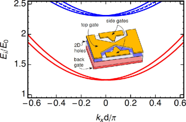
Here we present a study of charge transport induced by time-dependent SIA spin splitting in p-type (hole) quantum wires or point contacts, taking into account the special properties of hole states due to their effective spin-3/2 degree of freedom Yu and Cardona (1999). Figure 1 illustrates the basic device setup considered in our work. A quasi-one-dimensional (quasi-1D) hole system with free propagation direction for holes parallel to the axis is realized by engineering the appropriate quantum confinement in the orthogonal in-plane () direction of a p-type semiconductor heterostructure that has growth direction parallel to the axis. SIA spin splitting is modulated in time by means of front- and back-gate voltages Engels et al. (1997); *nitta:prl:97; *grund:prl:00 that generate an electric field parallel to the heterostructure-growth () direction. As for conduction electrons Governale, Taddei, and Fazio (2003), the time-dependent SIA spin splitting acts as a time-dependent and spin-dependent gauge field. The resulting spin-dependent electromotive forces generate oppositely directed and spin-polarized partial currents from spin-split subbands. To convert the induced spin current into a more easily measurable charge current, an in-plane magnetic field is applied perpendicularly to the quasi-1D system (i.e., in direction). As we will see below, the larger magnitude and favorable sample-parameter dependences of this current in hole systems make it more easily experimentally accessible than in n-type structures.
We use the Luttinger model Luttinger (1956) for the top-most valence band in common semiconductor materials. Within the spherical approximation Baldereschi and Lipari (1973), the corresponding effective-mass Hamiltonian for holes reads (we count hole energies as positive)
| (1) |
Here is the electron mass in vacuum, and the parameter measures the splitting between heavy-hole (HH) and light-hole (LH) bulk-valence-band dispersions in terms of the materials-dependent Luttinger parameters Vurgaftman, Meyer, and Ram-Mohan (2001). denotes the hole wave vector, and is the vector of spin-3/2 matrices Winkler (2003). The Zeeman coupling of hole spin to a magnetic field is described by , where denotes the Bohr magneton and is the isotropic hole g-factor.111We neglect the typically very small anisotropic contribution to Zeeman splitting in the valence band. SIA gives rise to a coupling between the holes’ orbital motion and their spin. The corresponding (Rashba) term in the Hamiltonian reads Winkler (2003) . The band-structure parameter Å2 in GaAs (values for other semiconductor materials can be found in Ref. Winkler, 2003), and is the effective electric field quantifying SIA.
Following the spirit of previous proposals for quantum pumps of conduction-band electrons Governale, Taddei, and Fazio (2003); Mal’shukov et al. (2003), we consider the holes to be confined in a quasi-1D system by a quantum-well confinement in direction and additional in-plane confinement . For simplicity, we assume the confining potential in both directions to be of hard-wall type, with respective widths and , and project onto quasi-1D bound states by setting , , , and , with integer and . This yields an effective Hamiltonian describing HH-LH splitting and mixing within the subspace of a single quasi-1D bound-state level. As SIA will typically only be sizable in the quantum-well growth direction, we have . Defining the abbreviation , as well as a natural energy scale , magnetic-field strength for GaAs, the SIA voltage scale ( V for GaAs), and , we find , with
| (2a) | |||||
| (2b) | |||||
| (2c) | |||||
| (2d) | |||||
Straightforward diagonalization of yields the spin-split quasi-1D hole-subband dispersions. See Figure 1.
HH-LH mixing between different orbital bound-state levels is neglected within our model. Such a simplified approach yields reliable results only for the lowest spin-split subband *[See; e.g.; ][; whereasimilarmodelforholepointcontactswasdiscussed.]uz:pssc:06. Hence, we limit our study to the case where only the two subbands with are occupied. Thus four propagation channels exist for holes in the device. Their corresponding Fermi wave numbers, denoted by for right-movers and for left-movers, are straightforwardly found from the subband dispersions.
To model the not necessarily perfect transmission of a hole point contact, we introduce a -barrier potential half-way between the two leads that make contact to the quasi-1D hole system of length . The scattering matrix is found by adapting standard methods Datta (1995) to the case of four-spinors describing spin-3/2 hole states.
Application of (front and/or back-gate) voltages can be used to effect a change in the SIA spin splitting Engels et al. (1997); *nitta:prl:97; *grund:prl:00 and should thus make it possible to impose a variation of with time . Under certain conditions, transport of charge and/or spin will be the result of such a time dependence Governale, Taddei, and Fazio (2003); Mal’shukov et al. (2003); *avishai:prl:10. To produce a dc charge current in the adiabatic regime, temporal variation of at least two parameters is necessary, whereas a time-dependent by itself only generates ac currents. Studying the latter will provide useful insight into the physical mechanism for spin-dependent quantum pumping and is also more easily possible experimentally. Hence we focus here on ac charge transport generated in situations where only SIA spin splitting is time-dependent.
Using techniques introduced in Ref. Büttiker, Thomas, and Prêtre, 1994 (see also Ref. Brouwer, 1998), currents injected in the leads are given in terms of contributions due to transmission and reflection coefficients. We label different blocks of the scattering matrix by and define partial currents as222These partial currents satisfy Onsager-type relations , , , , where the last two equations are valid for symmetric devices with the barrier placed midway between contacts.
| (3) |
Currents entering the left (L) and right (R) leads are then given by and . We consider the linear combination of left and right currents that is related to net charge transport between the two leads: .
For our chosen device geometry, is entirely due to spin-dependent electromotive forces. These arise because the wave function of charge carriers travelling between the leads acquires a dynamical phase that appears in the transmissions: and . As the wave vectors are functions of , they are time-dependent when SIA spin splitting is modulated. Time-dependent phases of transmission coefficients can be interpreted as electromotive forces that, in the present case, are also subband-dependent. This is the origin of the spin-orbit gauge-field contribution to , which scales linearly with . It turns out that all other contributions to cancel, and that the current is antisymmetric in . The antisymmetry of w.r.t. is the distinctive feature of charge transport generated by time-dependent spin-orbit gauge fields. This is so because spin-dependent electromotive forces generate oppositely directed partial currents from the two spin-split subbands whose imbalance in results in a finite transport current .

Figures 2 and 3 show the dependence of the spin-orbit gauge-field generated current on a number of experimentally relevant quantities. We use as the unit of current and scale current values by to absorb the linear dependence on .
The magnitude of as a function of the aspect ratio for the quasi-1D confinement is shown in Fig. 2. While there is a precipitous drop in current as deviates from one, it still remains finite in situations where the nature of the propagating states becomes more 2D-like.

Figure 3 elucidates the dependence of on the -barrier strength and, thus, on the transmission of the quasi-1D system. For comparison, we show our result for a hole system alongside two curves that are obtained for conduction electrons in the same material under the same conditions, with and without band nonparabolicity included. Two major differences between the conduction-electron and hole cases are apparent. Firstly, in the same semiconductor material, the maximum of for a p-type structure is two orders of magnitude larger than that for an n-type one. Secondly, the dependence on the barrier potential is qualitatively different in the two cases. For holes, the maximum occurs in the limit when the quasi-1D system is perfectly transmitting. In a point contact, this situation can be realized over a wide range of system parameters at the lowest conductance plateau. In contrast, the maximum transport current in conduction-electron systems appears for a non-unitary transmission value, and reaching it in a point contact requires fine-tuning of parameters in the narrow conductance-step region.
The strong enhancement and different qualitative behavior of for holes as compared with electrons can be traced back to the strong mixing between HH and LH states in a quasi-1D system. The resulting nonparabolicity of hole subbands increases the sensitivity of Fermi wave vectors and, hence, of quantum phases in the transmission amplitude, to time dependence of SIA spin splitting. Due to their special nature and comparable energy scales, HH-LH mixing and HH-LH splitting result in qualitatively different nonparabolicity effects than those present in conduction-electron systems. To illustrate this point, we show in Fig. 3 the transport current that is obtained when nonparabolicity in the conduction band Ogg (1966); Malcher, Lommer, and Rössler (1986) is taken into account *[Weusedtheconduction-band-structureparametersgivenin][.]cardona:jap:02 (dot-dashed curve) alongside the result for the same system with nonparabolicity neglected (dashed curve). It is seen that, for conduction electrons, nonparabolicity also enhances the ac charge current generated by spin-dependent electromotive forces, but the enhancement is only a fraction of the maximum current obtained in the parabolic approximation, and the general shape of the -dependence is similar in the cases with and without nonparabolicity. In particular, the current maximum still occurs at approximately the same finite value of barrier strength . This moderate influence of nonparabolicity in the conduction-electron case has to be contrasted with the drastically different shape of the curve obtained for a hole system.
In conclusion, charge currents flowing in quasi-1D hole systems in response to a time-varying SIA spin splitting are predicted to have a large magnitude (in GaAs, 200-times larger than for conduction electrons) due to strong spin-orbit effects in the valence band and because of subband nonparabolicity arising from HH-LH mixing. Proportionality to system size indicates the purely quantum origin of these currents, and their odd symmetry with respect to transverse in-plane magnetic fields enables unambiguous extraction of this special current component in experiments.
References
- Governale, Taddei, and Fazio (2003) M. Governale, F. Taddei, and R. Fazio, Phys. Rev. B 68, 155324 (2003).
- Mal’shukov et al. (2003) A. G. Mal’shukov, C. S. Tang, C. S. Chu, and K. A. Chao, Phys. Rev. B 68, 233307 (2003).
- Avishai, Cohen, and Nagaosa (2010) Y. Avishai, D. Cohen, and N. Nagaosa, Phys. Rev. Lett. 104, 196601 (2010).
- Engels et al. (1997) G. Engels, J. Lange, T. Schäpers, and H. Lüth, Phys. Rev. B 55, R1958 (1997).
- Nitta et al. (1997) J. Nitta, T. Akazaki, H. Takayanagi, and T. Enoki, Phys. Rev. Lett. 78, 1335 (1997).
- Grundler (2000) D. Grundler, Phys. Rev. Lett. 84, 6074 (2000).
- Winkler (2003) R. Winkler, Spin-Orbit Coupling Effects in Two-Dimensional Electron and Hole Systems (Springer, Berlin, 2003).
- Danneau et al. (2006) R. Danneau, W. R. Clarke, O. Klochan, A. P. Micolich, A. R. Hamilton, M. Y. Simmons, M. Pepper, and D. A. Ritchie, Appl. Phys. Lett. 88, 012107 (2006).
- Klochan et al. (2006) O. Klochan, W. R. Clarke, R. Danneau, A. P. Micolich, L. H. Ho, A. R. Hamilton, K. Muraki, and Y. Hirayama, Appl. Phys. Lett. 89, 092105 (2006).
- Rokhinson, Pfeiffer, and West (2006) L. P. Rokhinson, L. N. Pfeiffer, and K. W. West, Phys. Rev. Lett. 96, 156602 (2006).
- Shabani, Petta, and Shayegan (2008) J. Shabani, J. R. Petta, and M. Shayegan, Appl. Phys. Lett. 93, 212101 (2008).
- Csontos et al. (2010) M. Csontos, Y. Komijani, I. Shorubalko, K. Ensslin, D. Reuter, and A. D. Wieck, Appl. Phys. Lett. 97, 022110 (2010).
- Quay et al. (2010) C. H. L. Quay, T. L. Hughes, J. A. Sulpizio, L. N. Pfeiffer, K. W. Baldwin, K. W.West, D. Goldhaber-Gordon, and R. de Picciotto, Nat. Phys. 6, 336 (2010).
- Yu and Cardona (1999) P. Y. Yu and M. Cardona, Fundamentals of Semiconductors, 2nd ed. (Springer, Berlin, 1999).
- Luttinger (1956) J. M. Luttinger, Phys. Rev. 102, 1030 (1956).
- Baldereschi and Lipari (1973) A. Baldereschi and N. O. Lipari, Phys. Rev. B 8, 2697 (1973).
- Vurgaftman, Meyer, and Ram-Mohan (2001) I. Vurgaftman, J. R. Meyer, and L. R. Ram-Mohan, J. Appl. Phys. 89, 5815 (2001).
- Note (1) We neglect the typically very small anisotropic contribution to Zeeman splitting in the valence band.
- Zülicke (2006) U. Zülicke, phys. stat. sol. (c) 3, 4354 (2006).
- Datta (1995) S. Datta, Electron Transport in Mesoscopic Systems (Cambridge U Press, Cambridge, UK, 1995).
- Büttiker, Thomas, and Prêtre (1994) M. Büttiker, H. Thomas, and A. Prêtre, Z. Phys. B 94, 133 (1994).
- Brouwer (1998) P. W. Brouwer, Phys. Rev. B 58, R10135 (1998).
- Note (2) These partial currents satisfy Onsager-type relations , , , , where the last two equations are valid for symmetric devices with the barrier placed midway between contacts.
- Ogg (1966) N. R. Ogg, Proc. Phys. Soc. 89, 431 (1966).
- Malcher, Lommer, and Rössler (1986) F. Malcher, G. Lommer, and U. Rössler, Superlat. Microstruct. 2, 267 (1986).
- Städele et al. (2002) M. Städele, K. Hess, T. Ruf, and M. Cardona, J. Appl. Phys. 91, 9435 (2002).