Organic photovoltaic bulk heterojunctions with spatially varying composition.
Abstract
Models of organic bulk heterojunction photovoltaics which include the effect of spatially varying composition of donor/acceptor materials are developed and analyzed. Analytic expressions for the current-voltage relation in simplified cases show that the effect of varying blend composition on charge transport is minimal. Numerical results for various blend compositions, including the experimentally relevant composition of a donor-rich region near the cathode (a “skin layer” of donor material), show that the primary effect of this variation on device performance derives from its effect on photocharge generation. The general relation between the geometry of the blend and its effect on performance is given explicitly. The analysis shows that the effect of a skin layer on device performance is small.
I introduction
Photovoltaic devices consisting of two types of organic materials (referred to as donor (D) and acceptor (A)) have attracted considerable scientific interest in recent years. Their operation consists of the generation of an exciton in the donor molecule, which is then disassociated into free carriers at the D-A interface (the electron is transferred to the acceptor molecule’s lowest unoccupied molecular orbital (LUMO), leaving a hole in the donor molecule’s highest occupied molecular orbital (HOMO)). Carriers which avoid recombination are then collected by contacts. The geometry first studied consisted of single D and A layers, with a single planar interface tang . The resulting efficiencies were low (1 %), owing in part to the short exciton diffusion length (10 nm) - only excitons within this short distance from the interface lead to free carriers. It was subsequently discovered that blending D and A together throughout the device thickness led to increased efficiencies yu , now above 5 % eff1 ; eff2 ; eff3 . This increase in efficiency is attributed to an increase in D-A interfacial area; carrier transport is sufficiently robust to the disorder present in the blend to accommodate reasonable quantum efficiencies. If the organic blend is completely homogeneous, the contacts on the device must be different in order to break spatial symmetry and permit a nonzero short-circuit current in a preferred direction. The key difference between the contacts is their work function: a lower (higher) work function ensures that the contact preferentially collects and injects electrons (holes). Hence it is understood that the cathode collects electrons, and the anode collects holes.
A major thrust of experimental efforts has been to attain control over blend morphology in order to optimize both exciton disassociation and charge transport. Recent examples include using nanoimprint lithography to control the structure of the donor-acceptor molecules’ interfacial profile morph1 , or using a graded donor-acceptor blend to optimize both carrier collection and transport holmes . A key challenge of engineering blend morphology is the measurement and characterization of the structure of the organic blend. Techniques for accomplishing this include atomic force microscopy hamadani , ellipsometry germack , and X-ray photoelectron spectroscopy xu . These techniques have revealed that typical methods for fabricating devices lead to a layer of enhanced donor molecule density at the cathode, which has been attributed to surface energy differences between the active layer and other components xu . This would seem to present an impediment to good device performance: the cathode collects electrons, but in its vicinity is mostly holes! Nevertheless, internal quantum efficiencies of 90 % have been observed in these materials schilinksy , indicating that charge collection is still a relatively efficient process germack .
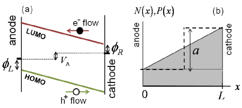
In this work, I theoretically study the effect of a nonuniform blend on organic photovoltaic (OPV) device performance. I employ a drift-diffusion equation to describe electron and hole transport, a field and temperature dependent generation and recombination rate that captures the exciton physics, and the Poisson equation for electrostatics. To this model I add the effect of a spatially varying effective density of states (EDOS) (note that “density of states” refers to the number of states per volume per unit energy, whereas “effective density of states” refers to the number of states per volume). Part I describes details of the model. In part II, I present analytic solutions for the transport under certain approximations; these point to the fact that the effect of a spatially varying EDOS on charge transport is small. In part III, I present numerical results which indicate that the primary effect of a spatially varying EDOS is on the charge generation and ensuing . It is shown that this can be understood in terms of the overall geometry of the composition profile. I conclude that since the skin layer near the cathode is geometrically small on the scale of the device thickness, its effect on performance is similarly small.
II Model
The model used to describe the system is similar to that found in Ref. koster, . Its basic equations are presented here in dimensionless form. Table I shows the variable scalings used. The dimensionless drift-diffusion/Poisson equations including a spatially varying EDOS are given as fonash :
| (1) | |||||
| (2) |
where is the ratio of hole to electron mobility, is the carrier density generation rate, and is the recombination. and are the spatially-dependent electron and hole effective density of states, respectively. and are related via: , where is the electron quasi-Fermi level, is the conduction band edge, and all quantities are position-dependent (the densities are assumed to be such that the system is in a nondegenerate regime). and are related similarly. and are fixed material parameters, while and are system variables that depend on applied voltage and illumination. For a single band semiconductor, the effective density of states is given by , where is the effective electron mass. In the present context of organic materials, is more properly understood as the number of HOMO states per unit volume, and is proportional to the donor molecule density.
| Quantity | Normalization |
|---|---|
| density | |
| position | |
| charge current | |
| electric potential | |
| rate density |
The boundary conditions are given as:
| (3) |
where is the device thickness (this represents placing the anode at , and the cathode at ). is the absolute value of the difference between HOMO (LUMO) and left (right) contact Fermi level. The boundary condition for the Poisson equation is:
| (4) |
where is the applied voltage (with the sign convention above, corresponds to forward bias).
I consider only bimolecular recombination, with (dimensionless) form:
| (5) |
where , and is the equilibrium electron (hole) density. The carrier generation rate density is taken to be spatially uniform. As described in Ref. koster , adding the exciton density as a system variable modifies the source term in Eq. (1):
| (6) |
where is the exciton density generation rate, and is a field and temperature dependent factor which represents the probability for an exciton to disassociate into free electron and hole koster ; braun . The field and temperature dependence is described by Braun’s extension of Onsager’s theory of ion disassociation in electrolytes onsager .
Charge recombination and generation also generally depend on the donor and acceptor effective density of states. The total source term of Eq. (1) (denoted here by ) is therefore of the generic form:
| (7) | |||||
The appropriate forms for and depend on several factors, such as the dependence of the optical absorption and D-A interface area on relative D-A composition.

III Analytic cases
The set of equations described in Eq. (1) can be solved analytically for limiting cases, which can provide some insight into the effect of a spatially varying EDOS on the transport. Two cases are considered here: the first is an exponentially varying EDOS (which can be extrapolated to a linearly varying EDOS), and the second is an abrupt, step-like change in the EDOS. I present both solutions first and discuss the physics they describe second.
In both cases the electric field is taken to be spatially uniform (so that ), and recombination is ignored. I suppose further that is constant, and independent of (that is, in Eq. (7)). The exponentially varying EDOS is parameterized as:
| (8) |
where ensures that the total number of states is independent of . Substituting the expressions for electron (hole) current density into the equation of continuity (Eq. (1)) results in a second order differential equation for the electron (hole) density (). For the EDOS of Eq. (8), the resulting general solution is:
| (9) |
where are determined by the boundary conditions of Eq. (3). From this solution the current density can be obtained directly.
I express the resulting current-voltage relation as a sum of dark current and light current:
| (10) |
Both light and dark currents are well described by expanding to lowest order in the spatial variation of EDOS parameter ; I take , and express the applied voltage dependence in terms of . is bigger than 1 in the region of interest footnote1 , leading to the further approximation that . It’s useful to express current-voltage relation in terms of that for a uniform EDOS and electric field:
| (11) |
The dark and light current for the exponentially varying profile of Eq. (8) is then found to be:
| (12) |
I next consider a step function form of . I use the following form:
| (15) |
The general solutions for each region () are of the form given by Eq. (9) with =0. In addition to the boundary condition Eq. (3), there’s an additional boundary condition for this EDOS of continuity of charge and current density at . Making the same approximations as above leads to the following dark and light current:
| (16) |
A number of interesting and relevant features emerge from these solutions: first, only even powers of appear in the expansions. This is a consequence of the symmetry built in to the system: when and , electron particle transport from left to right is equal to hole particle transport from right to left. In both the exponential and step-like cases above, holes encounter an expansion in the EDOS along their transport direction, which increases the hole current. Conversely, electrons encounter a constriction, which decreases the electron current. To linear order (and all odd orders) in the expasion/contraction parameter , these effects cancel each other so that the total charge current only appears with even powers of . If the electron/hole symmetry is broken, or the symmetry of the EDOS is reduced (by shifting the step away from the center of the device), then odd powers of are present (with prefactors whose magnitude reflects the degree of symmetry breaking).
The other relevant feature of Eqs. (12) and (16) is the small magnitude of the prefactor. Noting again that is generally larger than 1 for the applied voltages of interest to solar cells, it’s clear by inspection that the prefactors are much smaller than 1. This indicates that the effect on transport of a spatial variation of the EDOS is quite weak.

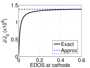
The intuitive picture that emerges from this analysis is that electrons and holes can very easily “squeeze” through regions of reduced density. A natural question concerns the way in which transport is ultimately “pinched off” by letting the density vanish at a point in space. This is shown in Fig. (2), which shows the current in the step-like structure as . The way in which the current vanishes is very steep; it is only at very small values of EDOS at the cathode that the current drops appreciably (in this limit, the approximation used in deriving Eq. (16) is not satisfied, hence the discrepancy between exact solution and Eq. (16)). However, for very small values of HOMO and LUMO density in real systems, the model presented here is likely not appropriate. This point is discussed more fully in the conclusion.
IV numerical studies
I next consider the effect of spatially varying EDOS when the Poisson equation for the electric potential and bimolecular recombination are included. Recall that the dependence of the generation and recombination on EDOS of electron and hole is described generically as:
| (17) |
I make the following ansatz for (the main conclusion can be formulated in a way that’s independent of this specific choice for ):
| (18) |
This is motivated by the observation that the D-A interfacial area requires both and , hence has a factor of each; an extra factor of is added since the exciton is initially generated in the donor. is taken simply to be 1, since already has and dependence built in through and . Adding a factor of to the recombination (so that the -dependence of both generation and recombination is the same) has only a weak effect on the results.
A range of composition profiles has been explored for the numeric evaluation of device performance, and I present two representative examples here:
| (19) | |||||
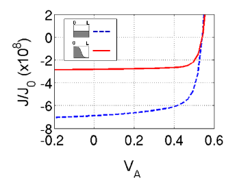
Fig. (3) shows the curves for the case (Eq. (IV)) for the uniform profile (), and a sharp S-shaped profile (). Note that the effect of the EDOS profile on the short circuit current is substantial, while the effect on open circuit voltage is small.

The previous analysis can explain the relative insensitivity of to a nontrivial EDOS profile: the effect of a varying EDOS profile on transport is weak, so that the injected current required to offset the photogenerated current (and the corresponding required voltage - ) is only weakly sensitive to changes in EDOS footnote2 .
The change in can be understood as a direct consequence of the model construction. is the current collected in the absence of an applied voltage, that is, in the absence of charge injected from the contacts. As such it is simply equal to the total charge generation rate in the device: . As described above, this is directly parameterized as:
| (21) | |||||
In analyzing the effect of on , it is instructive to separate the dependence of the generation from the above integral. This leaves a quantity which depends only on the geometry of the D-A EDOS profile:
| (22) | |||||
| (23) |
Strictly speaking the integral in Eq. (21) does not factorize in a manner that leads lead directly to a term. However, as I show in the following, is a good predictor of the effect of the geometry of the EDOS on the device performance.
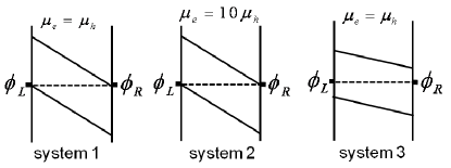
For each EDOS profile, I also vary other system parameters. The three different parameterizations are shown in Fig. (4). In system 1, HOMO/LUMO levels are aligned with cathode/anode Fermi levels (), and electron and hole mobility are equal. For system 2, , but electron and hole mobilities are not equal (). In system 3, the HOMO/LUMO are offset from cathode/anode by (), and electron/hole mobilities are equal.

Fig. (5a) and (5b) shows as the profile parameter is varied, for various EDOS configurations given by Eqs. (19) and (IV), respectively. This is shown for the three system parameterizations. The overall device efficiency tracks very closely for all of these cases (the efficiency is proportional to the maximum absolute value of in the 4th quadrant of the plane). For this reason I conclude that the primary effect of a spatially varying EDOS on device performance is to change the total carrier generation rate and ensuing . in Fig. (5) is calculated using Eq. (23), however the conclusion is valid for any choice of I’ve tried. Hence the effect of a nonuniform blend on performance can be approximately specified in the generic form given by Eq. (22).

Next I turn to the experimentally motivated geometry of a skin layer of D near the cathode. It’s parameterized as:
with , . Fig. (5c) shows how the efficiency evolves as the skin layer goes from mostly D-like (small ), to an even D-A mix, to mostly A-like (large ) (the experimentally realistic case is smaller ). The change in efficiency is a rather small effect for all three cases (a maximum of 10 % change). Also shown is the geometrical factor (solid line). The efficiency of system 1 conforms most closely to the geometrical factor profile dependence. Inspection of the curves for the three systems reveals subtle differences in the fill-factor between the three; there is no simple or obvious source for the difference in behavior between the three system parameterizations. The difference in behavior between the three systems is more conspicuous for the skin layer geometry because the effect of a nonuniform blend is smaller for the skin layer, so that the overall performance is more sensitive to other system parameters. (When the blend profile leads to larger effects, for example that shown in Fig. (5b), there is a similar dependence of device performance on profile for all system parameterizations.) Nevertheless, the important conclusion common to all three system parameterizations of the skin layer geometry is that the effect of the skin layer is small. Its smallness can be understood in terms of the analysis of the previous sections. The analytic work points to the fact that the effect of blend non-uniformity on charge transport is generically small (except in extreme cases). The numerical work of the previous test cases indicates that the effect of blend non-uniformity can be understood in terms of its effect on charge generation and resulting - and that this effect is essentially geometrical (see Eq. (22)). Since a skin layer is by definition geometrically small, its effect is similarly small.
V Conclusion
In this work I presented a simple model for the effect of nonuniform blend profiles on OPV device performance. The main effect of a nonuniform D-A blend is on the the charge generation and resulting short-circuit current: in regions where the blend is primarily of one type at the expense of the other, there is less charge generation due to a reduced D-A interfacial area. The details of how charge generation depends on local blend mix are complicated, and involve almost all aspects of OPV device operation (e.g optics moule , exciton diffusion holmes , etc.). The influence of a nonuniform blend on electron and hole transport is a weaker effect.
It’s important to appreciate the simplicity of the model presented here relative to the complexity of real OPV devices. Two simplifications of the model are: its treatment of the metal-organic interface, and its restriction to 1 spatial dimension. I make no attempt to capture the effect of a skin layer geometry on the metal-organic contact. The physics at this interface is included most simply as a finite recombination velocity scott (which can also depend on temperature and field lacic ). A hallmark of less effective charge collection/injection at this interface is S-shaped curves deibel . This feature is correlated to metal contact deposition techniques deibel , and is not ubiquitously observed in devices. I therefore conclude that the details of the metal-organic contact is not directly tied to the phase segregation in the organic blend.
A more severe approximation of this model is its restriction to 1-d. When the EDOS is small, the charge and current density is also small. However, experiments reveal localized hot-spots of conducting paths hamadani . A 1-d model necessarily averages these localized hot-spots or large current density over the entire cross-sectional area, leading to a diffuse current. As the overall area of hot-spots decreases, the charge and current density they must accommodate increases, and current may become space-charge limited. A 1-d model is unable to capture the physics described in this scenario. However for less extreme cases, the treatment described here offers the simplest account for a spatially varying blend structure.
I acknowledge very useful discussions with Behrang Hamadani and Lee Richter.
References
- (1) C. W. Tang. Two-layer organic photovoltaic cell. Appl. Phys. Lett. 48, 183 (1986).
- (2) G. Yu, J. Gao, J. C. Hummelen, F. Wudl, and A. J. Heeger, Science 270, 1789 (1995).
- (3) Jiangeng Xue, Barry P. Rand, Soichi Uchida, and Stephen R. Forrest. J. Appl. Phys., 9, 124903 (2005).
- (4) J. Peet, J. Y. Kim, N. E. Coates, W. L. Ma, D. Moses, A. J. Heeger, and G. C. Bazan. Nat. Mater. 6 497 (2007).
- (5) S. H. Park, A. Roy, S. Beaupre, S. Cho, N. Coates, J. S. Moon, D. Moses, M. Leclerc, K. Lee, and A. J. Heeger. Nat. Photon. 3 297 (2009).
- (6) D. Cheyns, K. Vasseur, C. Rolin, J. Genoe, J. Poortmans, and P. Heremans. Nanotechn. 19, 424016 (2008).
- (7) 1 R. Pandey and R.J. Holmes, Adv. Mater. 22, 5301-5305 (2010).
- (8) B.H. Hamadani, S. Jung, P. M. Haney, L. J. Richter, and N. B. Zhitenev, N.B. Nano letters 10, 1611 1617 (2010).
- (9) D.S. Germack, C.K. Chan, R.J. Kline, D.A. Fischer, D.J. Gundlach, M.F. Toney, L.J. Richter, and D.M. DeLongchamp, Macromolecules 43, 3828 (2010).
- (10) Z. Xu, L. Chen, G. Yang, C. Huang, J. Hou, Y. Wu, G. Li, C. Hsu, and Y. Yang, Advanced Functional Materials, 19, 1227 (2009).
- (11) P. Schilinsky, C. Waldauf, and C.J. Brabec, App. Phys. Lett. 81, 3885 (2002).
- (12) S. J. Fonash, Solar Cell Device Physics (Academic Press, Inc., London, 1981).
- (13) B. V. Andersson, A. Herland, S. Masich, and Olle Ingan as. Nano Lett. 9 853, (2009).
- (14) L. J. A. Koster, E. C. P. Smits, V. D. Mihailetchi, and P. W. M. Blom, Phys. Rev. B 72, 085205 (2005).
- (15) The most relevant region of the current-voltage relation is in the 4th quadrant. In this region, ; the different between and is scaled by , so that is generally much larger than 1.
- (16) The change in induced by a spatially varying EDOS has some effect on as well, but this is also a small effect, as generically varies only logarithmically with .
- (17) H. K. Gummel, IEEE Transactions on Electron Devices, 11, 455 (1964).
- (18) R. Sokel and R. C. Hughes, J. Appl. Phys, 53, 7414 (1982).
- (19) Adam J. Moulé, Jörg B. Bonekamp, and Klaus Meerholz, J. Appl. Phys. 100, 094503 (2006).
- (20) L. Braun, J. Chem. Phys. 80, 4157 (1984).
- (21) L. Onsager, J. Chem. Phys. 2, 599 (1934).
- (22) J.C. Scott and G.G. Malliaras, Chem. Phys. Lett. 299, 115-119 (1999).
- (23) S. Lacic and O. Ingana?s, J. Appl. Phys. 97, 124901 (2005).
- (24) A. Wagenpfahl, D. Rauh, M. Binder, C. Deibel, and V. Dyakonov, Phys. Rev. B 82, 115306 (2010).