The stability of graphene band structures against an external periodic perturbation ; Na on Graphene
Abstract
We report that the band of graphene sensitively changes as a function of an external potential induced by Na especially when the potential becomes periodic at low temperature. We have measured the band structures from the graphene layers formed on the 6H-SiC(0001) substrate using angle-resolved photoemission spectroscopy with synchrotron photons. With increasing Na dose, the band appears to be quickly diffused into background at 85 K whereas it becomes significantly enhanced its spectral intensity at room temperature (RT). A new parabolic band centered at 1.15 Å-1 also forms near Fermi energy with Na at 85 K while no such a band observed at RT. Such changes in the band structure are found to be reversible with temperature. Analysis based on our first principles calculations suggests that the changes of the band of graphene be mainly driven by the Na-induced potential especially at low temperature where the potential becomes periodic due to the crystallized Na overlayer. The new parabolic band turns to be the band of the underlying buffer layer partially filled by the charge transfer from Na adatoms. The five orders of magnitude increased hopping rate of Na adatoms at RT preventing such a charge transfer explains the absence of the new band at RT.
pacs:
73.21.-b,73.22.-f,71.10.PmI Introduction
Recent spur on the study of graphene has been motivated mostly by the unusual nature of its effectively massless charge carriers so-called Dirac fermions leading to some exotic electronic properties, its potential application for future nanometer-scale devices, on the other hand, has also been under extensive exploration. Graphene is a flat atomic single layer of graphite having a hexagonal crystalline symmetry with two atoms per unit cell. Its low energy band structure shows the almost linear bands with a vanishing density of states at the Dirac point of charge neutrality where the valence band ( band) and conduction band () meet at the K point of the hexagonal Brillouin zone. With increasing reports on the electronic properties of graphene layers including the anomalous quantum Hall effectsZhang05 ; Kane05 ; Li07 , the possibility of utilizing such features for atomic-scale devices seems to increase as seen also in the bilayer graphene Ohta07 . Ohta et al. show that the adsorption of Potassium on bilayer graphene modifies the potential symmetry in the graphene layers resulting in the change of energy gap at the K point. This provides a way of controlling the conductivity of the charge carriers for the switching capability in the atomic scale. Moreover recent calculations also provide a way to control the electrical properties of graphene by utilizing the chiral nature of the Dirac fermions of graphene.Park08 Park et al., show that the Dirac fermions of graphene can be quite sensitive to an external potential resulting, for example, the anisotropic renormalization of group velocity at the K point driven essentially by the chiral character of charge carriers of graphene. This feature becomes more prominent when the potential becomes periodic with a periodicity L comparable to that of the graphene lattice constant a1.42 Å. In addition, the life-time of Dirac fermions becomes significantly reduced when La0 by enhancing back-scatterings from the potential between states with momentums of and Ando1 ; Ando2 . No experimental study on the stability of graphene bands against a foreign perturbation, however, has been made especially for a potential with La0 despite several earlier angle-resolved photoemission spectroscopy (ARPES) studiesReinert ; Lanzara ; Gweon .
We report here an example of such a study that the presence of an external potential on graphene significantly affects the nature of Dirac fermions not only by the periodicity of the potential but also more remarkably by the degree of order of the potential especially when La0. We have investigated the behavior of the band along the direction as we adsorb Na on graphene at two different temperatures, 85 K and room temperature (RT). We find remarkable changes in the band as a function of Na dose at both temperatures. We also notice the appearance of a parabolic band centered at k=1.15 Å-1 only at 85K. Furthermore the band exhibits quite different behavior with Na on a bi-layer graphene from that of a single layer graphene. We mainly discuss such changes in the band of graphene in terms of the variation of the induced potential by Na adsorption. We also discuss the origin and characteristics of the new parabolic band from our band calculation.
II Methods
We have obtained our ARPES data by using the ARPES chamber at the beamline 3A2 of the Pohang Accelerator Laboratory in Korea using synchrotron photons of energy 34 eV. The chamber was equipped with a hemispherical Scienta R4000 electron analyzer which provides an overall energy resolution of 113 meV. All measurements were made with the chamber under 110-10 Torr. An n-type 6H-SiC(0001) substrate was pre-treated by annealing at 900 ∘C under the Si flux generated from a resistively heated Si wafer at 1150 ∘C to obtain the phase. We then continued to anneal the substrate further to obtain a carbon rich surface with the phase as reported earlier.** Single layer and bilayer graphenes were self-assembled when this precursor phase was annealed for an extended time period. We have used a commercial (SAES) getter source to deposit Na on the graphene surface and measured work function change to estimate Na coverage.
In order to interpret our band data, we have also performed ab initio pseudopotential total energy calculations with a plane-wave basis set.Cohen The exchange-correlation of electrons was treated within the generalized gradient approximation (GGA) as implemented by Perdew-Berke-Enzelhof.Perdew The cutoff energy for the expansion of wave-functions and potentials in the plane-wave basis was chosen to be 400 eV, and the Brillouin zone sampling was done with the Monkhorst-Pack special k-point method with a grid of 551 for the buffer layer phase. We used the projector augmented wave pseudopotentials as provided by the software package (Vienna Ab-initio Simulation Package).Kresse The atomic relaxation was carried out until the Helmann-Feynman forces were less than 0.02 eV/Å. The vacuum layer in the supercell used in our calculations is set to be 8 Å, which is enough to minimize the artificial interlayer interaction.
III Results and Discussions
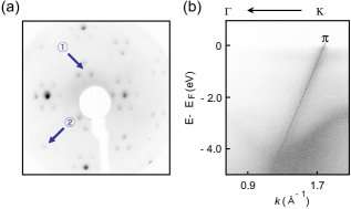
The phase of single layer graphene formed on SiC(0001) surface was first indicated by its characteristic LEED spots as seen in Fig. 1(a). While weakening the spots from the underlying phase (arrow 1), the LEED spots unique to the graphene phase (arrow 2) appear with growing intensity as annealing continued. A primary electron energy of 98 eV is used to monitor the changes in the LEED pattern during the preparation process. The electronic structure of the graphene thus prepared has been measured using ARPES along the direction of graphene up to the second Brillouin zone of the phase [see Fig. 5(b)]. Photoelectron intensity map near the zone boundary shows the well known graphene band [Fig. 1(b)] an indicative of a single layer graphene. This linear dispersion of the band suggests that the charge carriers in graphene can be considered as massless Dirac fermions. The single layer graphene suggested by LEED, however, has been finally confirmed by observing the unsplit linear band along the direction as shown in Fig. 1(b) before developing into the split band with further annealing due to the formation of multiple graphene layeres.Ohta07 Here we observe only one band rather than the two forming a conical shape band due to the chiral property of graphene.Shir95 ; Mucha07 From the slope of the band we estimate the Fermi velocity =1.10.074106 m/s in good agreement with earlier value of 106 m/s from Shubnikov-de Haas oscillationsNovo05 where the effective carrier mass of graphene was estimated to be about 0.02 0.07 with being the free electron mass.Novo05
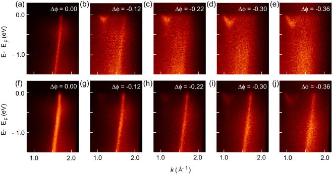
In Fig. 2, we show progressive changes of the band with increasing function of Na dose on a single layer (a-e) and a bi-layer (f-j) graphene at temperature 85 K. The amount of Na atoms adsorbed is indicated by work function change () induced by Na adsorption. The line-width of the band in (f) appears to be much broader than that in (a) of the single layer graphene. Although our resolution does not resolve the broadened band into two or more split bands, the measured line-width of 0.080.02 Å-1 indicates the band from a bi-layer graphene.Ohta07 From (a-e), one immediately notices that the adsorption of Na on the single layer graphene quickly deteriorates the band by significantly weakening its spectral intensity as well as broadening the line-width, and concomitantly accompanies a new parabolic band near Fermi energy. The deterioration of the band becomes worse while the parabolic band becomes stronger with increasing Na coverage. The corresponding changes induced by Na adsorption on the bi-layer graphene (f-j) are quite different from those on the single layer graphene; The band remains strong in intensity while slightly broadening with increasing Na dose. The parabolic band is still there but becomes much weaker compared to the one on the single layer graphene at the same dose of Na.
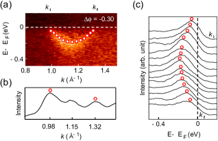
We first investigate the nature of the parabolic band. Figure 3 shows this new band at =0.30 eV. Red circles in Fig. 3(a) are the maxima in spectral intensity obtained by fitting the energy distribution curves (EDCs) with a Lorentzian function for 0.98 Åk1.32 Å-1 [see Fig. 3(c)]. The dispersion of the new band estimated from the momemtum distribution curve at Fermi energy in Fig. 3(b) appears to be parabolic with a minimum at 1.15 Å-1 for E=0.19 eV below the Fermi level. We obtain charge carrier mass m=0.580.07 and =3.40.41105 m/s, from the parabolic dispersion of the new band. The effective mass of charge carriers of this band is 8.329 times heavier than that of the Dirac electrons of the clean graphene without Na.
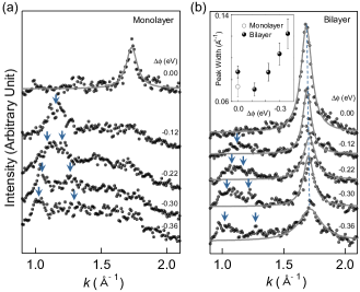
Interestingly, the band quickly fades away with the development of the new band as Na dose increases on the single layer graphene, which is more apparent in Fig. 4(a) where the momentum distribution curves (MDCs) change with Na dose. The band becomes almost disappeared into the broad background, whereas the new band enhances its spectral intensity showing the two peaks marked by arrows of the parabolic band centered at around 1.15 Å . The band, however, behaves quite differently with Na for the bi-layer graphene mostly maintaining its intensity as seen in Fig. 4(b). The rapid quenching of the band of the single layer graphene reflects a destructive effect associated with the Na adatoms on the top graphene layer. The sustaining intensity of the band from the bi-layer graphene in (f-j) may thus be attributed to the contribution from the second layer graphene overcoming the loss from the top graphene layer. This idea seems to be supported by the change of band width as a function of Na dose shown in inset of Fig. 4(b). The band width decreases initially down to the value of a single layer graphene and then begins to increase with further dose of Na. We will discuss later the possible causes of such changes of the band in Fig. 2.
We also performed ab initio pseudopotential total energy calculations with plane-wave basis set.Cohen The exchange-correlation of electrons was treated within the generalized gradient approximation (GGA) as implemented by Perdew-Berke-Enzelhof.Perdew The cutoff energy for the expansion of wave-functions and potentials in the plane-wave basis was chosen to be 400 eV, and the Brillouin zone sampling was done with the Monkhorst-Pack special k-point method with a grid of 551 for the buffer layer phase. We used the projector augmented wave pseudopotentials as provided by the software package (Vienna Ab-initio Simulation Package).Kresse The atomic relaxation was carried out until the Helmann-Feynman forces were less than 0.02 eV/Å. The vacuum layer in the supercell used in our calculations is set to be 8 Å, which is enough to minimize the artificial interlayer interaction.
Figure 5 shows the plausible binding site of Na atoms on the buffer layer in (a) and the Brillouin zones of the 11 of graphite together with those of the buffer layer in (b). With the Na coverage of 0.63 ML, the adsorption energy Ead calculated for the most favored site turns out to be 0.86 eV, compared to the next favored hollow site of 0.72 eV. All hollow sites of graphene appear to have Ead=0.73 eV. We note that the SiC surface is not completely covered with either single- or bi-layer graphenes.Ohta08 We find the most stable bonding configuration with a maximum adsorption energy Ead=1.03 eV when Na atoms form a single crystalline layer corresponding to the (110) plane of BCC Na as also seen in the scanning tunneling microscopy measurements of Na islands on graphite.Brei01
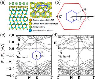
In Figure 5, we also present our band structures calculated with Na-added on the buffer layer in (c) and on the graphene layer in (d). One immediately finds the three partially filled bands near the point in (c) originating the upper two from the electrons in the buffer layer and the lower one from the Na adatoms. Since the buffer-layer bands are completely empty without Na adatomsKim07 , the bands of the buffer layer are rigidly shifted down by charge transfer from Na adatoms to the bands. The nearly empty upper bands in (d) then indicate that the charge transfer from Na occurs only to the top graphene layer with the underlying buffer layer almost intact. As depicted in Figure 5 (b) since the separation between the first () and second () Brillouin zones of the buffer layer is k=1.20 Å-1 much shorter than k=2.10 Å-1 of the Na (110) plane, the new parabolic band observed in Figure 2 must be the bands of the buffer layer partially filled by electrons from Na adatoms. The effective masses of the two buffer-layer bands are calculated to be 0.63 and 1.35 , respectively. We note that the effective mass of the upper one is quite close to the observed value of 0.580.07 . The relatively weak parabolic bands seen from the bilayer graphene in Figure 5 (f-j) may be caused by the reduced area of the exposed buffer layer compared to that of the single layer graphene.
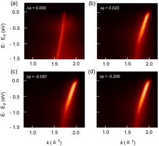
We now consider why the linear band of graphene deteriorates with Na adsorption. One may think of two plausible causes ; 1) due to the random scattering of photoelectrons from the disordered Na adatoms or 2) due to the reduced mean-free path of charge carriers by enhanced back-scatterings of charge carriers from a Na-induced periodic potential. The first cause, however, can be easily ruled out by our data in Fig. 6 showing the corresponding behavior of the band of graphene at RT. Here one immediately notices neither a new parabolic band nor the deterioration of the band with increasing Na. Instead, the band becomes stronger in intensity and shifts toward the higher binding energy by about 0.5 eV. Interestingly we find that the strong band at RT begins to deteriorate upon cooling the sample eventually reproducing the low-temperature features in Fig. 2. The change in the band of graphene with Na appears to be reversible in temperature. We thus attribute the second cause to the Na-induced weakening of the band of graphene assuming that Na adatoms form crystalline islands at low temperature giving rise to a certain form of a periodic potential.
If Na crystalizes at 85 K in the form of a layer corresponding to the (110) plane of BCC Na crystal as the Na islands formed on graphite,Brei01 the periodicity L of the Na-induced potential may be similar to a0 of the graphene lattice constant. Such a potential may severely modify the band structure in a way to reduce the mean-free path of charge carriers within graphene by enhanced back-scatterings of charge carriers as noted earlier.Park08 ; Ando1 ; Ando2 ; McEuen99 The formation of such crystalline Na islands at 85 K is indeed highly likely considering the significantly reduced hopping rate between the hollow binding sites (, where is an attempt frequency and is the Boltzmann constant), which is about 3.65105 times smaller than that at RT. Here we have used the diffusion barrier of 0.13 eV between the most stable hollow sites for Na on graphene. The stronger and shifted band at RT suggests that the band is shifted down rigidly towards the higher binding energy side revealing the highly occupied band near Fermi level as also observed when K is absorbed.Aaron On the other hand, the increased hopping rate of Na at RT drives delocalization of charge carriersAhn and reduces the donation of charges to the buffer layer leaving the band of the buffer layer empty as we find Fig. 6.
IV Conclusion
By adsorbing Na on graphene at two different temperatures (RT and 85 K) we observe that the band structure of graphene formed on SiC substrate becomes quite sensitively modified by the Na-induced periodic potential especially when the periodicity of the potential is comparable to the lattice constant of graphene. The frozen band of graphene quickly weakens in intensity and broadens in line-width with Na added at low temperature while it becomes stronger but is solidly shifted towards the higher binding energy with Na at RT. A new parabolic band observed only at 85 K by adding Na is found to be the band of the underlying buffer layer partially filled by the charges from Na. Such an extremely sensitive nature of Dirac fermions in graphene to external impurities as well as temperature demands a more careful study of transport properties of graphene for future practical applications in developing graphene based electronic devices.
Acknowledgements.
This work was supported by the Korea Science and Engineering Foundation (KOSEF) grant funded by the Korea government (MEST) by R01-2008-000-20020-0, and also in part by NCRC grant R15-2008-006-01001-0.References
- (1) K.S. Novoselov, A.K. Geim, S.V. Morozov, D. Jian, M.I. Katsnelson, I.V. Grigorieva, S.V. Dubonos, and A.A. Firsov, Nature 438, 197 (2005).
- (2) Y. Zhang, Y.-W. Tan, H.L. Stormer, and P. Kim, Nature 438, 201 (2005).
- (3) C.L. Kane and E.J. Mele, Phys. Rev. Lett. 95, 226801 (2005).
- (4) G. Li and E.Y. Andrei, Nat. Phys. 3, 623 (2007).
- (5) C.-H. Park, L. Yang, Y.-W. Son, M.L. Cohen, and S.G. Louie, Nat. Phys. 4, 213 (2008).
- (6) T. Ando and T. Nakanishi, J. Phys. Soc. Jpn. 67, 1704 (1998).
- (7) T. Ando, T. Nakanishi, and R. Saito, J. Phys. Soc. Jpn. 67, 2857 (1998).
- (8) Friedrich Reinert and Stefan Hüfner, New J. Phys. 7, 97 (2005).
- (9) A. Lanzara et al., Nature 412, 510 (2001).
- (10) G.-H. Gweon, T. Sasagawa, S.Y. Zhou, J. Graff, H. Takagi, D.-H. Lee, and A. Lanzara, Nature 430, 187 (2004).
- (11) M. Breitholtz, T. Kihlgren, S.-Å. Lindgrem, and L. Walldén, Phys. Rev. B 67, 235416 (2003).
- (12) E.L. Shirley, L.J. Terminello, A. Santoni, and F.J. Himpsel, Phys. Rev. B 51, 13614 (1995).
- (13) M. Mucha-Kruczyński, O. Tsyplyatyev, A. Grishin, E. McCann, VI. Fal’ko, A. Bostwick, and E. Rotenberg, Phys. Rev. B 77, 195403 (2008).
- (14) T. Ohta, A. Bostwick, J.L. McChesney, T. Seyller, K. Horn, and E. Rotenberg, Phys. Rev. Lett. 98, 206802 (2007).
- (15) M. Breitholtz, T. Kihlgren, S.-Å. Lindgrem, H. Olin, E. Wahlström, and L. Walldén, Phys. Rev. B 64, 073301 (2001).
- (16) I.R. Collins, A.R. Law, and P.T. Andrews, J. Phys. C: Solid State Phys. 21, L655 (1988).
- (17) T. Ohta, F. El Gabaly, A. Bostwick, J. McChesney, K.V. Emtsev, A.K. Schmid, T. Seyller, K. Horn, and E. Rotenberg, New J. Phys. 10, 023034 (2008).
- (18) I.W. Frank, D.M. Tanenbaum, A.M. van der Zande, P.L. and McEuen, J. Vac. Sci. Technol. B 25, 2558 (2007).
- (19) P. Simonis, C. Goffaux, P.A. Thiry, L.P. Biro, Ph. Lambin, and V. Meunier, Surf. Sci. 511, 3192 (2002).
- (20) P.L. McEuen, M. Bockrath, D.H. Cobden, Y.-G. Yoon, and S.G. Louie, Phys. Rev. Lett. 83, 5098 (1999).
- (21) M.L. Cohen, Phys. Scr. T1, 5 (1982).
- (22) J.P. Perdew, K. Burke, and M. Ernzerhof, Phys. Rev. Lett. 77, 3865 (1996).
- (23) G. Kresse and J. Hafner, Phys. Rev. B 49, 14251 (1994).
- (24) S. Kim, J. Ihm, H.J. Choi, and Y.-W. Son, Phys. Rev. Lett. 100, 176802 (2008).
- (25) Aaron Bostwick, Taisuke Ohta, Thomas Seyller, Karsten Horn, and Eli Rotenberg, Nat. Phys. 3, 36 (2007).
- (26) K. Rytkönen, J. Akola, and M. Manninen, Phys. Rev. B 69, 205404 (2004).
- (27) J.R. Ahn, K. Yoo, J.T. Seo, J.H. Byun, and H.W. Yeom, Phys. Rev. B 72, 113309 (2005).