Coherent Electron-Phonon Coupling in Tailored Quantum Systems
Abstract
The coupling between a two-level system and its environment leads to decoherence. Within the context of coherent manipulation of electronic or quasiparticle states in nanostructures, it is crucial to understand the sources of decoherence. Here, we study the effect of electron-phonon coupling in a graphene and an InAs nanowire double quantum dot. Our measurements reveal oscillations of the double quantum dot current periodic in energy detuning between the two levels. These periodic peaks are more pronounced in the nanowire than in graphene, and disappear when the temperature is increased. We attribute the oscillations to an interference effect between two alternative inelastic decay paths involving acoustic phonons present in these materials. This interpretation predicts the oscillations to wash out when temperature is increased, as observed experimentally.
Solid State Physics Laboratory, ETH Zurich, 8093 Zurich, Switzerland {addendum}
Correspondence and requests for materials should be addressed to P.R. (email: roulleau@phys.ethz.ch).
Coherent spin manipulation has already been accomplished in AlGaAs/GaAs double quantum dots (DQDs)[1, 2] and, more recently, also in InAs nanowires (NWs) [3]. While the coherence times are usually limited by random nuclear fields [4], also electron-phonon coupling can be a source of decoherence [5]. InAs nanowires (NW) and graphene are two alternative and promising materials for achieving coherent spin manipulation. In InAs NW DQDs, spin-orbit interactions (SOI) are very strong and enable a more efficient electron spin resonance driven by SOI compared to AlGaAs/GaAs DQDs [3]. In graphene, it is expected that hyperfine coupling as a source of decoherence is very weak compared to AlGaAs/GaAs. While electron-phonon interaction effects have been observed in carbon nanotube [6, 7], AlGaAs/GaAs [8], or silicon quantum dots (QDs) [9] and in AlGaAs/GaAs DQDs [10, 11], only little is known about electron-phonon interaction in graphene and InAs nanowires.
Almost 60 years ago, Dicke predicted superradiant and subradiant spontaneous emission [12], which was observed 40 years later with two trapped ions [13]. In this experiment, the spontaneous emission rate of a two-ion crystal excited by a short laser pulse was studied as a function of the ion-ion separation . Superradiant (subradiant) spontaneous emission was observed with (), where is the emission rate of a single ion. In analogy to the Dicke subradiance phenomenon, Brandes et al. [14] later proposed an interference effect due to electron-phonon interactions in a solid-state two-level system (DQD). Our experimental observations are interpreted in this framework.
Here we report on an effect associated with coherent electron-phonon coupling in two entirely different DQD systems and therefore different electronic and phononic environments. The very strong confinement of electronic states in these two materials, in contrast to AlGaAs/GaAs DQDs, has enabled us to observe this coherent coupling, the solid-state analogue of the Dicke subradiance phenomenon. Our measurements show periodic oscillations in the current through both double dot systems as a function of the energy difference of the levels in the two dots. The energy dependence of these oscillations allows us to infer a coherent coupling between electrons and the phonon field. We find an enhancement of the coherent oscillations in the InAs NW compared to graphene in agreement with dimensional considerations. The temperature at which the experimentally detected oscillations disappear ( 600 mK) clearly supports the relevance of a coherent effect in the coupled electron-phonon system. Finally, this study shows new possibilities for using graphene and InAs nanowires as nanoelectromechanical devices and, more specifically, as phonon detectors.
Results
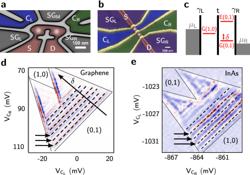
Observation of periodic oscillations. The two investigated
devices are shown in Fig. 1a (graphene) and Fig. 1b (InAs-NW). The
current through a DQD is maximal at triple points of the charge
stability diagram, where the electrochemical potentials of both dots
are degenerate and aligned with the electrochemical potentials of
source and drain [15]. The schematic configuration
of the DQD is illustrated by the energy level diagram in Fig. 1c. In
Figs. 1d and e, we show the numerical derivative of the current with
respect to and , , for one pair of triple points in each
material system. A bias voltage mV
(graphene) and 2.5 mV (NW) has been applied across the DQDs which
results in a triangular shaped region of allowed transport.
Along the baseline of the triangles (in Figs. 1d and e), the two ground-state levels G(1,0) and G(0,1) are aligned and . We can roughly estimate the number of electrons in each InAs NW dot to N 30. In graphene, a similar estimation is very difficult since we do not know exactly where the Dirac point is located. For a detuning , inelastic transitions are probed: if energy can be exchanged with the environment, a current flows as observed in Figs. 1d,e. A striking feature is the presence of periodic peaks parallel to the baseline, indicated by arrows in Figs. 1d,e, with a periodicity (graphene, first cool-down) and a smaller periodicity (NW). These periodic current modulations have been observed in different triangles, in both bias directions with equal periodicity, and in two different cool-downs (for graphene).
For a more detailed analysis of similarities and differences between graphene and InAs NW DQDs, the currents through the DQDs along the detuning line (indicated in Fig. 1d) have been measured (Fig. 2) in a different triangle. As in the previous measurement, we observe that the periodicity in graphene is larger (270 eV) than in the InAs NW (200 eV). The periodic peaks are more pronounced in the InAs NW than in graphene. In total we have measured 4 pairs of triple points for different gate configurations in graphene and have extracted for the first cool-down and for the second cool-down. In the InAs NW we have measured 19 different triple points, 15 being in a range . These values are much smaller than the typical excited state energies which are several meV above the ground state (see Figs. 2a and b), due to the small effective mass [16, 17]. In graphene, measurements realized a in single dot of similar size show excitations at energies of around 2-4 meV [18, 19]. In the measured device we see current steps superimposed on the periodic current oscillations at energies of 2 meV. We attribute the stepwise current increase to the opening of additional transport channels due to excited states, with comparable energies as measured in single dots. In the following, we provide evidence that our observations are related to an interference effect.

Features of the coherent coupling. To understand these observations, we model inelastic transitions which occur in a DQD. We first suppose that for inelastic transitions phonons are emitted [11]. Therefore, the transition rates are proportional to the Bose-Einstein coefficient. For graphene, the coupling of acoustic phonons to electrons is due to deformation potential coupling [20, 21, 22].
The double dot is modeled as a two level system with a bonding state and an antibonding state with . We are interested in transitions between these two states due to the absorption or emission of acoustic phonons. The relevant matrix element for this process is , where arises from the Hamiltonian that describes the electron-phonon coupling. Emission and absorption rates due to the deformation potential coupling can be written as [23]
| (1) |
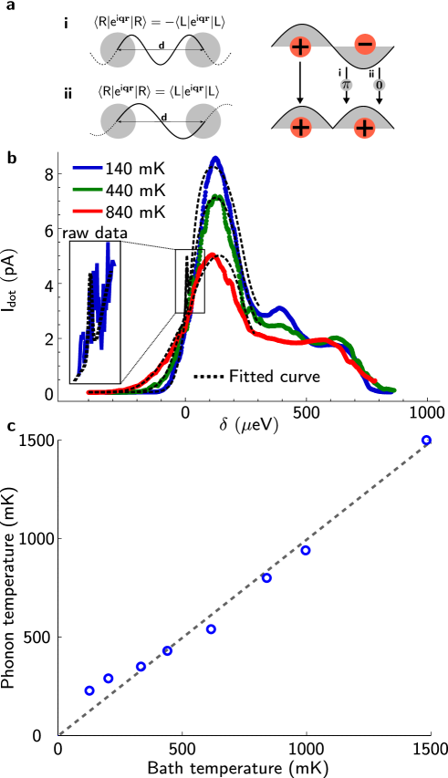
where is the single atom mass, the number of atoms in the system and the energy splitting between the two levels. In order to simplify , we make two assumptions. First, we neglect the overlap between the electronic wave functions of the two dots, which is equivalent to saying that the cross terms can be neglected compared to the direct terms . This gives , i.e. there are two alternative decay paths. In a second step, we assume that =, where describes a state localized in the left dot which typically has an exponential decay at the dot boundaries, and = the state in the right dot, with d being the distance vector between the two dots. From this we obtain the relation . We finally have , and therefore . This expression predicts periodic oscillations in the emission rate as a function of quasi-momentum q, which can be interpreted as an interference effect in which the electron relaxes in either the left or right dot, analogous to the Dicke subradiant spontaneous decay [12, 14]. The phase difference between the two interfering paths is related to the phonon wave function and the opposite parity of ground- and excited state (see Fig. 3a).
The periodicities in graphene allow to extract a distance between the two dots of nm (first cool-down) and nm (second cool-down) for a sound velocity of (25% below the theoretical predictions [21]) and nm for a sound velocity [16] in the InAs NW DQD. In both cases, our results are in agreement with the geometry of the DQDs (in the graphene DQD, we have measured a mutual coupling energy meV (first cool down) meV (second cool down) in agreement with a larger effective distance between the two dots for the second cool down).
In a recent pioneering experiment realized in an InAs NW DQD with a diameter of 50 nm [16], similar equidistant peaks with a separation eV were observed. The authors argue that these resonance lines result from a modified phononic energy spectrum due to the strong radial confinement. Following this argument we should observe a separation eV in our measurements, considering that our NW is thicker (130 nm). Instead, we measure (at different triple points and for different gate configurations) eV. We also find that the periodicity is strongly affected by the electrostatic potential of our gates (not shown), although the phonon energy spectrum should not depend on the electronic environment. Thus we conclude that the interpretation related to simple phonon confinement [16] cannot explain our measurements. Nevertheless our interference-based approach could be in agreement with C. Weber et al.’s observations of a separation of eV.
Comparison between InAs nanowire and graphene. The measurements of Figs. 2c and d indicate that the interference effect is more pronounced in the InAs NW than in graphene. Different mechanisms could lead to such an observation. For instance, the assumption of localized electronic wavefunctions without overlap could be less relevant in graphene leading to a damping of the oscillations. In addition to this, the dimensionality of the system could influence the amplitude of the interference. In a 2D system for example, the oscillatory part will be proportional to , where is the sound velocity and is the angle between the quasi-momentum q and the distance vector d. In an ideal 1D system we would obtain a factor which implies more pronounced interference. Theoretical calculations which compare the phonon spectrum in a graphene and in an InAs NW DQD are needed to further clarify this point.
Signatures of a bosonic environment. In the solid-state environment of our DQDs, temperature is expected to antagonize interference effects by destroying coherence. In the phonon absorption and emission rates (equation 1), temperature only appears through the Bose-Einstein distribution with , , and = where is the energy difference between the bonding and antibonding state, the tunnel coupling between the dots, and = - the energy difference between left and right states [24]. Measurements of the current through the graphene DQD close to eV for different temperatures are shown in Fig. 3b. We observe a clear dependence of the inelastic transitions on temperature, and as expected the current for negative detuning is enhanced at elevated temperatures since absorption is more pronounced when the temperature is increased.
For more quantitative predictions, we calculate the expected current through the DQD: the rate equations for the occupation of the states can be expressed as a function of the tunnel coupling, (left barrier), (right barrier), (emission), and (absorption), allowing to calculate the stationary solution [25]. The stationary current is plotted as a function of detuning in Fig. 3b (dashed line) for a bath temperature of 140 mK. The good agreement with the measured curve enables us to extract a phonon temperature 230 mK. The discrepancy between bath and phonon temperatures disappears when the mixing chamber temperature is increased, as can be seen in Fig. 3c, where the extracted phonon temperatures are plotted as a function of bath temperature. Above 300 mK, bath and phonon temperatures are in excellent agreement. This result confirms an energy-exchange with the phonon bath.
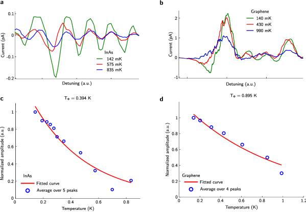
Temperature dependence. In Figs. 4a and b, we plot the current oscillations for InAs and graphene DQDs, respectively, for temperatures from 140 mK up to 1 K. We note a continuous decrease of the peak amplitudes with increasing temperature. These observations confirm the difference compared to the interpretation in Ref. [16]: current replica due to the interaction between electrons and individual phonon modes should not depend strongly on temperature below 1 K (eV K).
The extracted temperature dependence of the average amplitude for the first 5 peaks (normalized by the lowest temperature amplitude) is presented in Figs. 4c. The red solid line is a exp(/-fit to our data with mK as discussed below. A similar dependence is observed in graphene (Fig. 4d) with mK.
Discussion.
To explain this temperature dependence, we
consider decoherence: we suppose that the phase difference between
the two interfering emission processes is not perfectly defined due
to coupling to the thermal bath. In the limit where the thermal
energy is large compared to the energy equivalent of the transition
time scales (=̂ eV in our case), phase fluctuations are given
by the fluctuation-dissipation theorem and the visibility of
the oscillations decays exponentially over a characteristic
temperature :
=
[26]. The quantity quantifies the
strength of the thermal fluctuations the electron is experiencing in
the interferometer (see Fig. 3a). Since decoherence of the phonon
wave function is quite unlikely, we think that with increasing
temperature bonding and antibonding states are washed out. However,
theoretical calculations are needed to validate this hypothesis.
In conclusion, we have observed an oscillatory effect in transport through DQDs in graphene and in an InAs NW which we attribute to coherent electron-phonon coupling in nanostructured geometries. The characteristic phase difference for this interference is determined by the phonon field phase difference between both dots. We have observed that the effect is more pronounced in an InAs NW compared to a graphene DQD. Finally, we have shown that the temperature dependence of these oscillations is compatible with a thermal decoherence mechanism. This study may contribute to a better understanding of the role of the phonon bath in electron transport through NWs and graphene DQDs.
Fabrication. The procedures to fabricate our graphene quantum system are described in Refs. [27, 28]. The InAs NW, grown by metal organic vapor-phase epitaxy, is deposited on a predefined Hall bar of an AlGaAs/GaAs heterostructure with a two-dimensional electron gas (2DEG) 37 nm below the surface. The etching mask for the DQD and detector structure, realized by electron beam lithography, is designed in such a way that the trenches in the 2DEG forming the detectors and the constrictions in the NW are aligned (see Fig. 1b) [29]. Applying a voltage between each detector and the corresponding QD enables us to control the electrochemical potentials of the QDs [30]. In order to tune the tunnel barriers independently, the trenches in the 2DEG are additionally filled with metallic top gates (AlOx/Al/Ti/Au). The two dots have a lithographic dimension of roughly 100 nm for the graphene DQD and 130 nm for the InAs NW. The measurements were performed in two different dilution refrigerators at 120 mK (base temperature).
References
- [1] Petta, J. R. et al. Coherent Manipulation of Coupled Electron Spins in Semiconductor Quantum Dots. Science 309, 5744 (2005).
- [2] Koppens, F. H. L. et al. Driven coherent oscillations of a single electron spin in a quantum dot. Nature 442, 766-771 (2006).
- [3] Nadj-Perge, S., Frolov, S. M., Bakkers, E. P. A. M., Kouwenhoven, L. P. Spin-orbit qubit in a semiconductor nanowire. Nature 468, 1084 1087 (2010).
- [4] Bluhm, H.et al. Dephasing time of GaAs electron-spin qubits coupled to a nuclear bath exceeding 200 s. Nat. Phys. (advance online publication), 1038 (2010).
- [5] Hayashi, T., Fujisawa, T., Cheong, H. D., Jeong, Y. H. & Hirayama, Y. Coherent Manipulation of Electronic States in a Double Quantum Dot Phys. Rev. Lett. 91, 226804 (2003).
- [6] Leturcq, R. et al. Franck-Condon blockade in suspended carbon nanotube quantum dots. Nat. Phys. 5, 327-331 (2009).
- [7] Escott, C. C., Zwanenburg, F. A., & Morello, A. Resonant tunnelling features in quantum dots. Nanotechnology 21, 274018 (2010).
- [8] Weig, E. M. Single-Electron-Phonon Interaction in a Suspended Quantum Dot Phonon Cavity. Phys. Rev. Lett. 92, 046804 (2004).
- [9] Zwanenburg, F. A., van Rijmenam, C. E. W. M., Fang, Y., Lieber, C. M. & Kouwenhoven, L. P. Spin States of the First Four Holes in a Silicon Nanowire Quantum Dot. Nano Lett. 9, 1071-1079 (2009).
- [10] Naber, W. J. M., Fujisawa, T., Liu, H. W. & van der Wiel, W. G. Surface-Acoustic-Wave-Induced Transport in a Double Quantum Dot. Phys. Rev. Lett. 96, 136807 (2006).
- [11] Fujisawa, T. et al. Spontaneous Emission Spectrum in Double Quantum Dot Devices. Science 282, 932 (1998).
- [12] Dicke, R. H. Coherence in Spontaneous Radiation Processes. Phys. Rev. 93, 99 (1954).
- [13] DeVoe, R. G. & Brewer, R. G. Observation of Superradiant and Subradiant Spontaneous Emission of Two Trapped Ions. Phys. Rev. Lett. 76, 2049 (1996).
- [14] Brandes, T. & Kramer, B. Spontaneous Emission of Phonons by Coupled Quantum Dots. Phys. Rev. Lett. 83, 3021 (1999).
- [15] Hanson, R., Kouwenhoven, L. P., Petta, J. R., Traucha, S. & Vandersypen, L. M. K. Spins in few-electron quantum dots. Rev. of Mod. Phys. 79, 1217- 1264 (2007).
- [16] Weber, C., Fuhrer, A., Fasth, C., Lindwall, G., Samuelson, L. & Wacker, A. Probing Confined Phonon Modes by Transport through a Nanowire Double Quantum Dot. Phys. Rev. Lett. 104, 036801 (2010).
- [17] Pfund, A., Shorubalko, I., Ensslin, K. & Leturcq, R. Spin-state mixing in InAs double quantum dots. Phys. Rev. B 76, 161308(R) (2009).
- [18] Schnez, S. et al. Observation of excited states in a graphene quantum dot. Appl. Phys. Lett. 94, 012107 (2009).
- [19] Güttinger, J. et al. Electron-Hole Crossover in Graphene Quantum Dots. Phys. Rev. Lett. 103, 046810 (2009).
- [20] Bolotin, K. I., Sikes, K. J., Hone, J., Stormer, H. L, & Kim, P. Temperature-Dependent Transport in Suspended Graphene. Phys. Rev. Lett. 101, 096802 (2008).
- [21] Hwang, E. H. & Das Sarma , S. Acoustic phonon scattering limited carrier mobility in two-dimensional extrinsic graphene. Phys. Rev. B 77, 115449 (2008).
- [22] Vasko, F. T., & Ryzhii, V. Voltage and temperature dependencies of conductivity in gated graphene. Phys. Rev. B 76, 233404 (2007).
- [23] Rossler, U. Solid State Theory, (Springer, 2009).
- [24] Oosterkamp, T. H. et al. Microwave spectroscopy of a quantum-dot molecule. Nature 395, 873 (1998).
- [25] Gasser, U. et al. Statistical electron excitation in a double quantum dot induced by two independent quantum point contacts. Phys. Rev. B 79, 035303 (2009).
- [26] Stern, A, Aharonov, Y., Imry, Y. Phase uncertainty and loss of interference: A general picture. Phys. Rev. A 41, 3436 (1990).
- [27] Molitor, F. et al. Transport through graphene double dots. Appl. Phys. Lett. 94, 222107 (2009).
- [28] Molitor, F. et al. Observation of excited states in a graphene double quantum dot. Europhys. Lett. 89, 67005 (2010).
- [29] Shorubalko, I. et al. Self-aligned charge read-out for InAs nanowire quantum dots. Nano Lett. 8, 382 (2008).
- [30] Choi, T., Shorubalko, I, Gustavsson, S., Schön, S. & Ensslin, K. Correlated counting of single electrons in a nanowire double quantum dot. New J. Phys. 11, 013005 (2009).
We thank A. Fuhrer, A. Wacker and U. Gasser for helpful discussions.
The experiments were conceived and carried out by P.R., S.B., T.C., F.M., J.G., T.M. and S.D. The InAs DQD was fabricated by T.C and P.R and the graphene DQD realized by F.M. The data were analysed by P.R., S.B. and F.M. The manuscript was written by S.B. and P.R. The whole project was supervised by P.R, K.E. and T.I.
The authors declare that they have no competing financial interests.