Self-limited oxide formation in Ni(111) oxidation
Abstract
The oxidation of the Ni(111) surface is studied experimentally with low energy electron microscopy and theoretically by calculating the electron reflectivity for realistic models of the NiO/Ni(111) surface with an ab initio scattering theory. Oxygen exposure at 300 K under ultrahigh-vacuum conditions leads to the formation of a continuous NiO(111)-like film consisting of nanosized domains. At 750 K, we observe the formation of a nano-heterogeneous film composed primarily of NiO(111) surface oxide nuclei, which exhibit virtually the same energy-dependent reflectivity as in the case of 300 K and which are separated by oxygen-free Ni(111) terraces. The scattering theory explains the observed normal incidence reflectivity of both the clean and the oxidized Ni(111) surface. At low energies of the oxidized surface is determined by a forbidden gap in the projected energy spectrum of the bulk NiO crystal. However, for both low and high temperature oxidation a rapid decrease of the reflectivity in approaching zero kinetic energy is experimentally observed. This feature is shown to characterize the thickness of the oxide layer, suggesting an average oxide thickness of two NiO layers.
pacs:
68.37.Nq, 81.65.Mq, 71.15.ApI Introduction
Surface oxidation is an almost ubiquitous phenomenon, and it is generally associated with profound changes in geometrical structure and materials properties. The late transition metals (TMs) have received persistent attention Reuter (2007) owing to their tremendous importance in a variety of heterogeneously catalyzed chemical reactions. Kung (1989) The general oxidation mechanism may be qualitatively quite successfully described by the Cabrera-Mott modelCabrera and Mott (1948) developed more than 60 years ago, from which many common oxidation phenomena, e. g., the temperature-dependent thickening of oxide films until saturation, can be rationalized. Atkinson (1985) However, the different elemental properties of the TMs, arising from the varying -band occupation through the elemental series, give rise to a huge diversity in oxidation pathways, Reuter (2007) and here, using the oxidation of Ni as an example, we present a case where even this fundamental concept of oxide saturation thickness increasing with temperature needs to be rephrased.
A prominent example is the interaction of molecular oxygen with Ni(111), which is frequently viewed as a model system for dissociative adsorption of molecular oxygen on a TM surface. Numerous studies have already targeted the initial adsorption of oxygen onto clean Ni(111), which induces a (22) surface reconstruction.Conrad et al. (1975); Kortan and Park (1981)
While the structural model of this low-coverage phase, which is established upon low O2 exposure, is well accepted, there is no general consensus regarding the structure of the nickel oxide layers that form with prolonged oxygen dose. An especially interesting case is the range of sample temperatures above 600 K during oxidation, which has so far remained mostly unexplored. Below 600 K, different scenarios have been proposed depending on temperature, involving the evolution of few-layer-thick, bulk-like NiO filmsHolloway and Hudson (1974); Tyuliev and Kostov (1999); Hildebrandt et al. (2000); Okazawa et al. (2007) or the formation of individual oxide grainsCornish et al. (2010); Muñoz-Márquez et al. (2004) of thicknesses exceeding 10 nm. Muñoz-Márquez et al. (2004)
Due to this inherent complexity of surface oxidation at its early stages, deeper insight into the underlying physical and chemical processes may be gained from information gathered in situ, i. e., acquired in real time during reaction in an oxidative environment. Ideally, the experimental tools of choice should enable a simultaneous surface-sensitive characterization of geometrical and concomitant electronic structure, establishing a link between the two properties.
A promising approach to real-time studies of dynamic surface processes in TM oxidation Altman and Bauer (1996); J. P. Pierce and K. F. McCarty (2005); Pierce et al. (2008); Flege and Sutter (2008); Flege et al. (2008); Flege and Sutter (2009) is to employ scattering of low-energy electrons in full-field microscopy, also known as low-energy electron microscopy (LEEM).Bauer (1994); Altman (2010) This method is intrinsically sensitive to the near-surface region owing to the strong interaction of slow electrons with condensed matter, and it provides microscopic insight on a length scale of a few nanometers. Information on the surface crystal structure is accessible by the related technique of low-energy electron diffraction (LEED), which allows to determine the dimension of the surface unit cell and the point group of the lattice. In addition, for a given reflected beam the dependence of the reflected current on the acceleration voltage of the incident electrons, the curve, contains information on the structure of the unit cell. The atomic arrangement on the surface can be inferred from the multiple-scattering analysis of the curves for several reflected beams over a wide energy range.Pendry (1974); van Hove and Tong (1979) This technique, commonly referred to as intensity-voltage, -LEED, has already enabled the determination of many surface structures.Heinz et al. (2008) The curves also reflect the bulk electronic structure, in particular, the Bragg gaps and critical points, where the band structure strongly deviates from free-electron-like behavior. Jaklevic and Davis (1982); Strocov et al. (1996) This effect is especially pronounced at low energies, where the inelastic scattering is rather weak.
Experimentally, the much higher intensity of the reflected electron current at very low energies in the range of a few eV, typical of LEEM measurements, makes it very attractive to record the dependence in a spatially and time-resolved manner by sampling the electron energy in imaging mode. This so-called -LEEM technique facilitates the measurement of the individual dependence of nanosized surface phases and has already been applied to processes in epitaxial growth,Hannon et al. (2006) surface chemical reactions,Schmid et al. (1995) and oxidation catalysis.Flege and Sutter (2008); Flege et al. (2008)
However, despite the achievements of the well-established techniques in the interpretation of LEED at the energies of a few tens of eV, their application at very low energies is not straightforward: most of the implementations of the multiple scattering theory rely on a rapid decay of the electron wave into the solid, while at the energies of a few eVs the inelastic scattering is weak, and the penetration depth is very large. In addition, low-energy electrons are rather sensitive to details of the crystal potential, Krasovskii and Strocov (2009) so for a fully conclusive comparison with the experiment the LEED calculation should rely on the self-consistent potential – in the sense of density functional theory (DFT) – both in the bulk and at the surface.
In the present work we present a combined experimental and theoretical study of the energy-dependent conduction properties of oxygen overlayers on Ni(111) with the aim to relate the observed curves to the electronic properties of the surface and, eventually, to its atomic structure. We apply an ab initio scattering theory based on a full-potential augmented-plane-waves (APW) formalism to a model of the oxidized Ni(111) surface. A good agreement between the calculated and the measured LEED spectra allows us to interpret the spectral structures and to conclude on the thickness of the surface oxide layer. In particular, we find a forbidden energy gap in the projected spectrum of the (111) surface of the bulk NiO crystal, which causes a rapid increase of electron reflectivity from the oxidized Ni(111) surface at low kinetic energies. We show that with decreasing thickness of the oxide layer the electron transmission does not increase uniformly over the gap region, but a narrow transmission channel opens at the bottom of the gap, which is observed in our measurements.
The paper is organized as follows: In Secs. II and III, we describe the experimental procedures to oxidize the pristine Ni(111) surface and characterize the oxygen-rich phases in situ. The theoretical approach is introduced in Sec. IV, and applied to Ni(111) and to thin NiO layers on Ni(111) in Secs. V and VI, respectively.
II Experimental Details
Most experiments were conducted at the National Synchrotron Light Source (NSLS) at Brookhaven National Laboratory (BNL), Upton, NY (USA) using the spectroscopic photoemission and low-energy electron microscope (LEEM III including hemispherical energy analyzer, Elmitec) installed at beamline U5UA.Flege et al. (2007) Additional LEEM measurements were performed in the newly-installed LEEM III system (Elmitec, no energy filter) at our home institute at the University of Bremen. Transferability of the results was cross-checked and asserted by performing experiments under nominally identical conditions.
A commercially purchased, polished Ni(111) single crystal (Mateck) with a nominal orientation better than was used. After insertion into the UHV chamber the sample was cleaned by several cycles of 0.5 keV Ar+ ion sputtering followed by thermal annealing at 1050 K. In addition, short flashes to 1300 K were found to improve the smoothness of the surface on the nano- to sub-micrometer scale. Surface cleanliness following this recipe was already asserted in an earlier study.Meyer et al. (2010) Sample temperatures are given based on the reading of a W/Re thermocouple permanently attached to the sample support. In the oxidation experiments, research-grade (99.998%) oxygen (Matheson Tri-Gas Co.) was dosed from a high-precision leak valve in back-filling mode. The BNL-LEEM and the Bremen-LEEM systems exhibited base pressures of Torr and Torr, respectively.
The kinetic energy of the incident electrons in all curves presented in this article is referenced to the onset of the mirror electron mode, i. e., with respect to the vacuum level. Experimentally, this onset has been measured by determining the inflection point of the abrupt edge in sample reflectivity observed when increasing the electron energy to a few eV.
III Experimental Results and Discussion
III.1 Ni oxidation and NiO structure: status quo
We begin by briefly reviewing the present status quo for oxidation of Ni(111). Depending on oxygen dose, Ni(111) has been found to undergo a (22) surface reconstruction for coverages up to monolayer (ML) [for Ni(111), 1 ML corresponds to an atomic density of cm-2] followed by nucleation of an epitaxial oxide layer for larger oxygen exposures.Holloway and Hudson (1974); Conrad et al. (1975); Kortan and Park (1981) At room temperature, oxidation has been reportedTyuliev and Kostov (1999); Okazawa et al. (2007) to start upon an accumulated dose larger than 10 Langmuir (L) (1 L amounts to Torrs). A three-stage model of the process has been proposed, Holloway and Hudson (1974, 1974) involving (i) dissociative chemisorption, (ii) nucleation of oxide islands exhibiting a thickness of a few atomic layers, and (iii) slow thickening of the oxide film.
Depending on sample temperature during oxidation, different NiO orientations have been identified. Below 470 K, only NiO(111) formation has been observed,Conrad et al. (1975); Kitakatsu et al. (1998); Hildebrandt et al. (2000); Okazawa et al. (2007) while NiO(001) islands have been found for more elevated temperatures.Christensen et al. (1986); Kitakatsu et al. (1998); Hildebrandt et al. (2000) These findings have been rationalizedChristensen et al. (1986) based on the thermodynamic instability of the unreconstructed NiO(111)-(11) surface, which, because of its rocksalt structure and within a picture of purely ionic bonding, should carry a diverging dipole moment.Tasker (1979) Since the NiO(111) films were experimentally determined to be very thin, i. e., only a few atomic layers thick, a metastable character of the NiO(111) orientation has been postulated, in agreement with the growth of the thermodynamically stable, unpolar NiO(001) face at 500 K, i. e., at sufficiently high temperature.Christensen et al. (1986) In other studies, the stability of the NiO(111)-(11) surface has been related to the adsorption of hydroxyl speciesRohr et al. (1994); Kitakatsu et al. (1998) that prevent the surface from undergoing a so-called “octopolar” (22) reconstruction leading to a compensation of the surface dipole.Wolf (1992); Barbier et al. (2000) Since hydroxyl species are easily removed by annealing to 600 K,Rohr et al. (1994) this scenario would provide an alternative explanation for the stability of the (11) phase at room temperature and the preferential growth of NiO(001) above 500 K.Kitakatsu et al. (1998) Yet, it has still remained unclear whether the driving force for the (22) reconstruction at high temperature would be the same for thinVentrice, Jr. et al. (1994) as well as moderately thick NiO(111) films—a question raised almost twenty years ago.Rohr et al. (1994)
Quantitative information on actual oxide thickness, however, has proven difficult to obtain, and substantial variations in oxide “saturation thickness” have been reported depending on both temperature and oxide phase. At 300 K, several studies have concluded on an oxide thickness of a few monolayers for the NiO(111) layer.Holloway and Hudson (1974); Christensen et al. (1986); Kitakatsu et al. (1998); Okazawa et al. (2007) In the case of NiO(001), this saturation thickness may extend to more than 10 nm according to medium-energy ion scattering (MEIS)Muñoz-Márquez et al. (2004) after exposure to O2 at 500-600 K, which has been noticed to grow at a considerably higher rate.Christensen et al. (1986)
Based on MEIS,Muñoz-Márquez et al. (2004) it has also been postulated that, in the elevated oxidation temperature range, the NiO/Ni interface is very rough, consisting of irregularly shaped NiO grains, and indeed multiple oxygen-enriched grains have been seen in photoelectron microscopy with oxygen-sparse areas in between.Cornish et al. (2010) However, until the present the high-temperature oxidation regime above 500-600 K has remained largely unexplored with respect to atomic and nanoscale structure.Haugsrud (2003)
In the following Secs. III.2 and III.3, we present our results for Ni(111) oxidation at 300 K and 750 K. In the former case, we find the formation of a tight patchwork of nanosized NiO(111) domains. The corresponding spectrum exhibits a very strong, characteristic peak at about 6 eV. At a sample temperature of 750 K, which is significantly higher than the temperature range explored so far, we observe essentially the same local curve for the oxidized parts of the Ni(111) surface concomitant with a local (11) LEED pattern, corroborating the nucleation of ultrathin (111)-oriented oxide domains even at these high oxidation temperatures.
III.2 Oxidation pathway at room temperature
Following the cleaning recipe outlined in Sec. II, a clean, well-ordered Ni(111) surface is established exhibiting only steps and step bunches in LEEM (see Fig. 1(a)). Surface crystallinity is asserted by a sharp (11) LEED pattern (Fig. 2(a)). Afterwards, the sample was exposed to molecular oxygen (O2) at a background pressure of Torr while the modification of the surface was monitored by LEEM (Fig. 1) and LEED (Fig. 2). After dosing O2 for 13 s, which corresponds to an accumulated dose of 1 Langmuir (L), the integral sample reflectivity has considerably decreased, as can be deduced from Fig. 1(b). This change in intensity is accompanied by the advent of a (22) reconstruction in LEED (Fig. 2(b)), which is expected for a nominal oxygen coverage of about ML.Kortan and Park (1981)
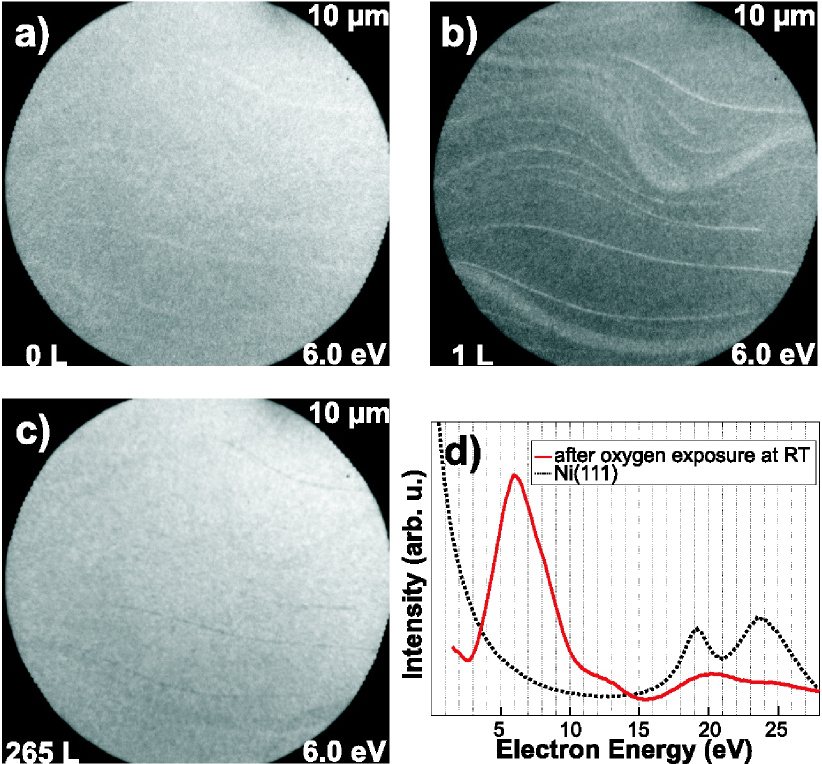
However, in addition to the integral change in reflectivity, we observe significant local variations of the (00) intensity at structural defects (see Fig. 1(b)) that do not contribute to the periodic part of the LEED pattern. While the terraces exhibit a rather low reflectivity at the chosen kinetic energy of the incident electrons ( eV), the steps appear significantly brighter in contrast. Since these white regions eventually fill the entire surface upon prolonged exposure (Fig. 1(c)),111In this subfigure (just as in Fig. 1(a)), the steps appear darker due to a very slight “underfocusing” condition for the objective lens, a setup which is very frequently used in LEEM to image substrate steps on otherwise homogeneous surfaces. we may attribute these bright areas to the formation of a more oxygen-rich surface phase that is associated with a distinct LEED pattern (Fig. 2(c)) of apparent six-fold symmetry but increased lattice parameter as compared to clean Ni(111). Further dosing of O2 does not induce any visible changes, neither in the reflectivity nor in the sample morphology. Nevertheless, we note an overall grainy appearance of the surface, suggesting the presence of structural features just below the resolution limit of the microscope.
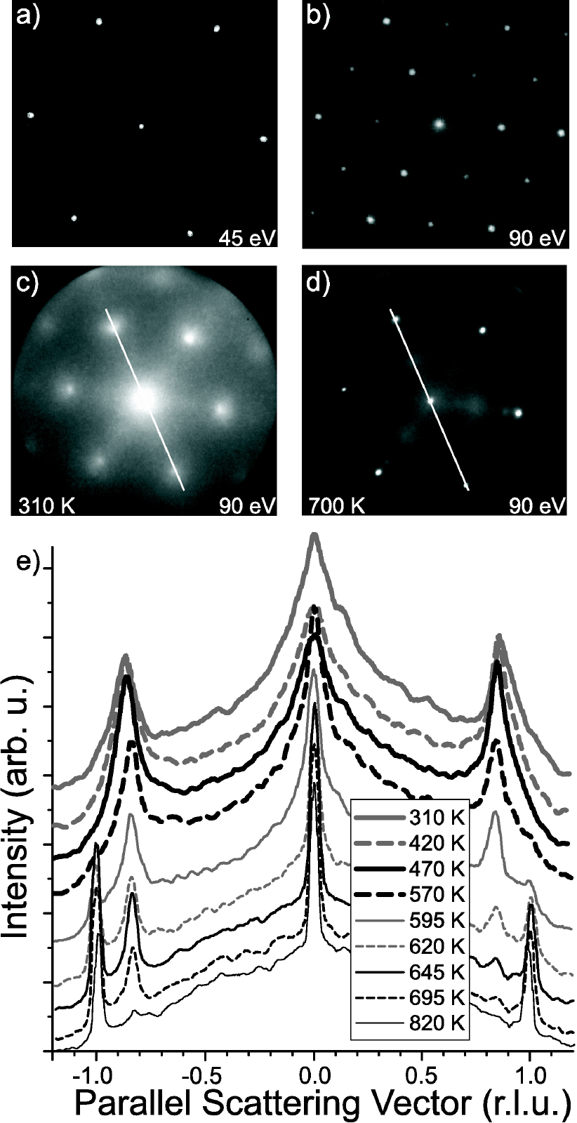
In the following sections, we will mainly focus both experimentally and theoretically on the structural identification of this bright phase. A comparison of data (Fig. 1(d)) acquired for the clean Ni(111) surface with the bright, homogeneous area readily corroborates the notion of a distinct phase. Further insight into the crystallographic structure is accessible by the quantitative analysis of line profiles extracted from LEED patterns recorded during thermal annealing from 300 K to 820 K. While no LEED spots associated with the Ni(111) substrate are found after preparation at 300 K, which confirms the presence of a continuous, oxygen-rich “film”, these integral order reflections re-appear at elevated temperature and clearly dominate the LEED pattern at 700 K (Fig. 2(d)), whereas the spots of the oxide film have almost vanished. Interestingly, additional spots emerge at half-order positions, underlining the formation of a (22)-O adlayer phase upon film disintegration and concomitant thermal desorption of oxygen atoms. A quantitative evaluation using the post-anneal pattern as reference reveals a lattice parameter of Å for the film, which is in good agreement with the lattice constant of bulk NiO(111) ( Å), Fievét et al. (1979) indicating an almost fully relaxed NiO film. Furthermore, from the width of the (11) peaks at 300 K, an average domain size of approximately nm can be deduced.
In separate experiments, room temperature grown NiO(111) films were annealed in a step-wise manner under other identical conditions in LEED as well as LEEM mode. With increasing temperature, the oxide peaks become slightly sharper while losing intensity (Fig. 2(e)). Comparable integral intensities of the oxide and substrate LEED spots are observed at about 620 K. This behavior suggests an Ostwald-like ripening process, in which smaller patches either dissolve or coalesce to form larger oxide islands, which yet remain too small to be imaged in LEEM mode. These findings confirm the results of a scanning tunneling microscopy study that reported an increase in domain size by about a factor of two after annealing to 700 K.Kitakatsu et al. (1998) Finally, at a temperature of 820 K, these islands have completely disappeared, and the original LEED pattern of the clean substrate is restored.
Summarizing, the presented LEED data strongly suggest the formation of a continuous NiO(111)-like film, which is composed of many small domains of a few nanometers in diameter. The recorded curve provides more information on the local crystallographic structure, which will theoretically be addressed in Sec. VI, but at this point it may already serve as a fingerprint for a NiO(111)-like phase in the upcoming oxidation studies performed at elevated temperature.
III.3 Oxidation at 750 K
The LEEM time-lapse sequence for oxygen exposure at a sample temperature of 750 K is depicted in in Fig. 3. On the clean surface (Fig. 3(a)) only steps and step bunches are visible. However, after a 9 L dose we note a qualitatively different behavior as compared to the previous case of oxidation at room temperature. Under the present conditions, islands exclusively nucleate at step bunches whereas the single steps and flat terraces remain unaffected. Apart from any morphological objects on the terraces, we do not find a large-scale change in reflected intensity as we observed for oxidation at room temperature. This qualitatively different result is confirmed by comparing the fingerprint of the terraces after an exposure of about 1000 L (Fig. 4(c)), e. g., extracted at point “A” in Fig. 4(a), with the reference spectra for the clean Ni(111) surface (Fig. 1(d)). Since the curves are virtually identical, this result clearly shows that only a negligible amount of chemisorbed oxygen is found on the terraces at this high temperature. Given the comparatively large oxygen doses needed to achieve substantial surface coverage, the integral dissociative sticking coefficient for molecular oxygen has to be substantially lower than at room temperature, in agreement with previous studies that targeted Ni(111) oxidation kinetics.Holloway and Hudson (1974)
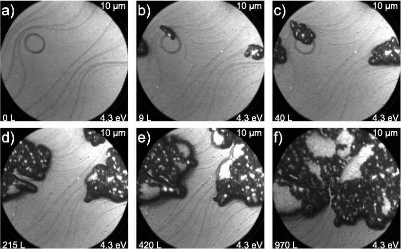
The few existing oxide nuclei, however, grow upon prolonged exposure and gradually spread over the remaining Ni(111) terraces, while the crossing of step bunches is not observed. We also note that essentially no additional, isolated nuclei appear on a 10 m scale (Fig. 3(b-e)), which is indicative of a significantly enhanced diffusion length of the oxygen species. Interestingly, the reacted areas are by no means single-crystalline domains of nickel oxide, but instead are composed of a variety of small grains exhibiting different contrast and irregular shapes. From the time-lapse sequence (Fig. 3(b-f)), we conclude that the edges of the already oxygen-rich areas serve as effective nucleation centers for subsequently grown oxide islands, a phenomenon that has already been observed in oxidation studies of other TM surfaces, e. g., Ru(0001).Flege and Sutter (2009) Because the lateral growth rate remains steady but slow throughout the remainder of the integral oxygen dose of about 1000 L (Fig. 3(f)), a considerable fraction of surface area remains unreacted to oxygen, in accordance with the intensity variations found in oxygen concentration maps at temperatures of 573 K and 673 K.Cornish et al. (2010)
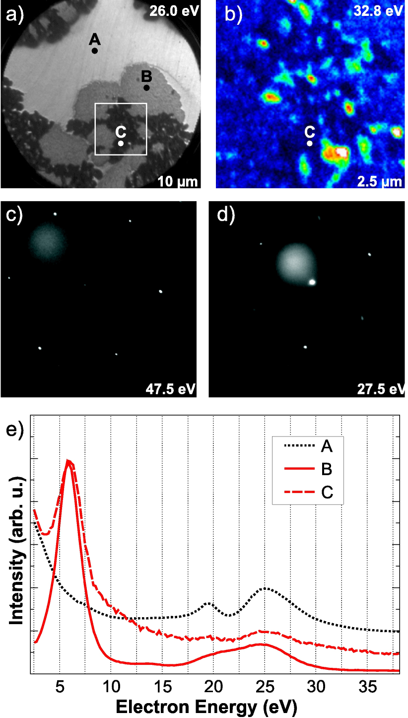
In Fig. 4(a), three main contrast levels are observed, one for the oxygen-free Ni(111) terraces and two in the oxide-covered areas. Hence, it would appear that mainly two types of oxide domains have nucleated, labeled “B” and “C” in the figure. The magnified view shown in Fig. 4(b), which is a blow-up of the center region indicated in Fig. 4(a), illustrates that the transformed areas are composed of a tight network of nanosized oxide patches exhibiting different contrast, but whose structural properties are nevertheless amenable to analysis. A comparison of the individual spectra of these oxygen-rich phases, using phases “B” and “C” in an exemplary fashion, reveals that they are closely related since they all show a very similar characteristic resonance at about 6 eV (Fig. 4(e)). Moreover, the curve for “B” is virtually identical to the one observed for oxidation at room temperature (Fig. 1(d)). Thus, we may already speculate at this point that all types of patches are some form of NiO(111), but apparently differ with respect to certain structural details.
Further insight is gained from selected-area LEED patterns acquired for all regions individually. While the local diffraction pattern for “A” (Fig. 4(c)) exclusively exhibits the expected (11) spots of the clean Ni(111) surface, the micro-LEED pattern for region “B” (Fig. 4(d)) shows a well-defined, three-fold (11) periodicity, whose surface unit cell is rotated by 30∘ with respect to the substrate lattice. A quantitative analysis of the peak positions indicates a lattice mismatch of 19%, in very good agreement with the presence of a completely relaxed NiO(111) film that shares a different registry with the substrate as compared to our observations at room temperature. Additionally, for relatively low electron energies we also noticed weak, very broad, and threefold-symmetric facet spots (not shown), which will be subjected to temperature-dependent investigations using micro-LEED and high-resolution LEED.Flege et al. Interestingly, we observed qualitatively similar diffraction patterns for both region types “B” and “C” that only differed by the relative intensities of the NiO(111) spots and the broad facet streaks. These findings suggest the presence of a tight, complicated mosaic structure consisting of well-aligned and, probably, considerably tilted NiO(111) domains for both types of regions, albeit exhibiting different areal ratios of the untilted versus the tilted regions. In this structural model, the measured shape of the curve for region “C” would then represent the sum of the individual curves of minuscule, untilted NiO(111) regions as well as of tilted NiO(111) regions, with the latter barely contributing to the integral intensity of the specular (00) beam.
Previous studiesChristensen et al. (1986); Kitakatsu et al. (1998) argue that for growth temperatures of about 500 K, only the (001) orientation of NiO should be present. Using our in-situ technique, we indeed observe NiO(001) formation in an intermediate temperature range of about 500 K (Ref. Flege et al., ), but based on the micro-LEED evidence in connection with the strong similarity of the curves presented here we clearly show that this is not the case for even higher temperatures of about 750 K, where NiO(111) is again prevalent. These results are in agreement with previous findings of a higher thermal stability of the NiO(111) films as compared to the NiO(001) in annealing experiments, in which the latter was shown to decompose upon annealing to 550 K.Kitakatsu et al. (1998)
It should be stressed, however, that we did not observe any signs of a (22) reconstruction of the oxide domains, clearly demonstrating that a NiO(111)-(11) structure that is rotated by 30∘ with respect to the Ni(111) substrate lattice is still stable at a temperature of 750 K. Evidently, the change in registry adds to the stability of these NiO(111) domains at temperatures close to decomposition of the room temperature grown oxide.
IV Computational Methodology
There exist two major approaches to an ab initio treatment of electron scattering by the surface. The more traditional multiple-scattering Green’s function method Pendry (1974); van Hove and Tong (1979) employs a representation of the crystal by a finite number of atomic monolayers. It has an advantage of avoiding the calculation of the partial Bloch waves inside the crystal and proceeds immediately to the scattering solution. Pendry (1976) This method is especially efficient within the muffin-tin approximation (MTA) for the crystal potential — although full-potential Green’s function methods have existed for many years Butler et al. (1992) the MTA is still widely used in the theory of LEED. Rundgren (2003) In the present work we use the alternative Bloch wave approach: the LEED function inside the crystal is sought as a linear combination of the partial waves, which facilitates the interpretation of the LEED spectra in terms of the band structure of the substrate.
To calculate the reflected intensities the LEED wave function is obtained as a solution of the Schrödinger equation for a semi-infinite crystal, see Fig. 5. The scattering wave function is defined by its energy and the incidence direction of the electron beam. In the plane parallel to the crystal surface obeys the Bloch theorem and is characterized by the 2D Bloch vector . In the vacuum, far from the crystal surface, it is a superposition of the incident plane wave and reflected (propagating and evanescent) plane waves. Deep in the crystal the potential is periodic, and in the absence of inelastic scattering (electron absorption) the partial waves are propagating (real ) and evanescent (complex ) Bloch waves that comprise the complex band structure of the semi-infinite crystal. Heine (1963) Then, the scattering problem consists in finding the coefficients of the partial waves.
The evanescent waves carry zero current, and the electron beam is completely reflected whenever falls in a -projected band gap. To take into account inelastic processes, which reduce the reflectivity, an imaginary term, the optical potential , is added to the potential in the crystal half-space. The energy is kept real, so the absorbing potential leads to a spatial damping of the wave functions, i. e., Bloch vectors of originally propagating waves acquire an imaginary part. Hence, electron absorption is allowed for, and even in the energy gaps of the bulk band structure there is no complete reflection anymore. Slater (1937) On average, increases with energy, and an approximate dependence can be inferred from the curvature of the measured curve. Krasovskii and Strocov (2009); Krasovskii et al. (2002) In the present case we used a linear function chosen so as to approximately reproduce whenever possible the sharpness of the peaks. An example for Ni(111) is shown in the inset of Fig. 6(d).
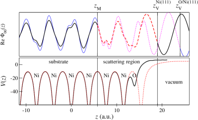
The computation starts with constructing self-consistent potentials in the bulk crystal and at the surface within the local density approximation (LDA) of the DFT. The band structure is calculated with the extended linear augmented plane wave method (ELAPW), using the full-potential augmented Fourier components technique. Krasovskii et al. (1999) The potential at the surface is determined by a repeated-slab calculation. The slabs comprise nine atomic layers and are separated by a vacuum region of 16 a.u., see Fig. 5. No structure optimization is performed: all atoms occupy the positions of the ideal Ni or NiO lattice, see Fig. 8.
The partial Bloch waves are obtained as solutions of the inverse band structure problem: for a given energy and they satisfy the Schrödinger equation in the bulk of the crystal. The calculations are performed with the ELAPW- method, which reduces the equation to a matrix eigenvalue problem, with being the eigenvalues. Krasovskii and Schattke (1997) To the left from the matching plane , see Fig. 5, the LEED function is a linear combination of several (only the waves with not exceeding 1 a.u.-1 are included).
In the surface region, between and , the potential is different from the bulk potential, and the partial waves representation is not valid. Here the function is expanded in terms of the eigenfunctions of the slab, which contains the scattering region, see Ref. Krasovskii, 2004. The functions , thus, have already taken into account the scattering by the overlayers. For each energy the three representations are matched at the two planes and to construct a smoothly continuous function that satisfies (with certain accuracy) the equation in the embedded region. (The Schrödinger equation is satisfied by construction both in the bulk and in the vacuum half-spaces.)
V Clean Ni(111)
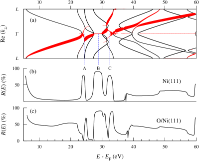
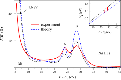
The ability of the substrate to conduct current can be characterized by the current carried by individual Bloch waves . For the clean Ni(111) surface the complex band structure in the direction and the energy-momentum distribution of the current are shown in Fig. 6(a). The current carried (absorbed) by an individual Bloch wave is shown by the thickness of the dispersion curves. Below 23 eV and above 34 eV relative to the Fermi energy the behavior of the main conducting branch is close to free-electron-like, i. e., the electron transmission is effected by a single bulk band with almost parabolic dispersion. Between 23 eV and 34 eV, there is a wide Bragg gap centered at 28 eV and a number of special points, where the conducting branch switches from one bulk band to another. They give rise to the sharp peaks A, B, and C in the elastic (i.e., ) spectrum of Ni(111). In the present experiment only the peaks A and B are visible (in agreement with earlier work, Ref. Jaklevic and Davis, 1982). This is explained by a strong effect of the inelastic scattering on the peak C. Figure 6(d) compares the measured spectrum (specular reflectivity) for clean Ni(111) to the calculations with realistic values of the optical potential. The theoretical curve is the ratio of the specularly reflected current to the incident current, and the experiment is the arbitrarily scaled curve. At moderate values of eV the peak C completely disappears, in agreement with the experiment. The theoretical curves in Fig. 6(d) are shifted by 1.6 eV to higher energies in order to bring the peaks A and B to the measured positions. This discrepancy is the result of the quasi-particle self-energy being inaccurately treated in the present calculation: the LEED functions are calculated as Kohn-Sham solutions in the local density approximation. The self-energy effect is seen to stretch the unoccupied spectrum by 1.6 eV over the interval of 30 eV.
VI NiO(111) crystal and films
To illustrate the effect of a thin overlayer on the electron reflection from Ni(111), we have presented in Figs. 5 and 6(c) calculations for an oxygen monolayer fully commensurate with the substrate (thereby strongly compressively strained in the lateral direction if single-layer NiO(111) is used as reference). Figure 5 compares the LEED functions for a clean Ni(111) surface and for an oxygen overlayer on Ni(111) at a kinetic energy of 10 eV. Already at the second Ni layer the wave function is seen to acquire the character of the substrate Bloch wave, but the oxygen overlayer reduces its amplitude. The comparison of the spectra in Figs. 6(b) and 6(c) shows that in the interval 7–22 eV, where the band structure of the substrate is free-electron-like, the oxygen overlayer increases the specular reflectivity to as much as 50%. However, its presence does not result in any sharp structures in this energy interval: the reflectivity steadily increases at low kinetic energies similar to the case of clean Ni(111). On the contrary, the measured spectrum of the oxidized surface, Fig. 1(d), shows a sharp decrease at low kinetic energies.
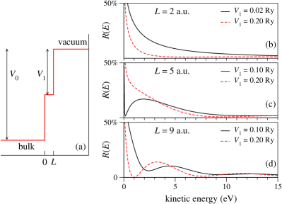
Naturally, at low energies the electron reflection is very sensitive to the shape of the potential barrier between the crystal half-space and the vacuum. This can be illustrated by a simple one-dimensional system, Fig. 7(a), in which the potential barrier is modeled by a two-step function. For a step-like potential barrier of height [with , in the notation of Fig. 7(a)], the electron reflection steadily decreases with energy: . However, when the width of the surface layer (with a different potential ) is increased up to several atomic units, the curve becomes non-monotonic, and at low energies transmission resonances appear – minima that characterize the surface layer. In the following, we will present an interpretation of the experimentally observed low-energy structure in the curve for an oxidized Ni(111) surface as caused by a thin oxide layer.
Because the formation of more than one NiO layer in the Ni(111) lattice is improbable, we now consider the more realistic situation where the oxidized surface layers have the structure of bulk NiO (see Fig. 8). In view of the large lattice mismatch between the Ni substrate and the surface NiO layers, to construct a fully realistic model of the oxidized surface is beyond our computational capabilities. However, we can make use of the observation that in the 15 eV wide energy region above the surface barrier, Ni(111) has a free-electron-like band structure. Hence, we can model the underlying crystal by an expanded lattice of Ni, with the same lattice constant as NiO. Because the expanded Ni(111) crystal too has a free-electron-like conduction band below eV, this model appears quite plausible at low energies and capable of providing a qualitative understanding of the effect of the Ni substrate.
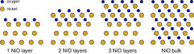
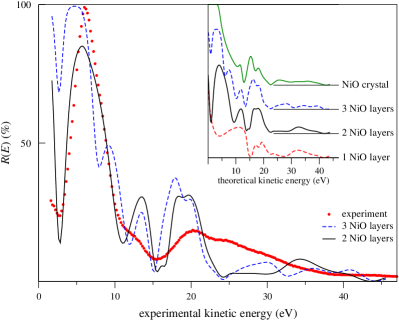
We have performed calculations of for one, two and three NiO layers on the model Ni substrate, as well as for bulk NiO(111) (cf. Fig. 8), which are shown in the inset of Fig. 9: apart from the region of very low kinetic energies, the gross features of the curve are determined by the outermost NiO layers: the raise of the reflectivity below 12 eV is caused by the NiO overlayer, and the reflection from the Ni-NiO interface brings about only relatively weak wiggles. However, for the few-layer thin surface oxides, in contrast to bulk NiO, in approaching the vacuum level the reflectivity rapidly falls down to produce a very sharp minimum, in agreement with our measurements, where it is found at about 2.7 eV above the vacuum level. This dip is a signature of the conducting substrate: the bulk energy spectrum of NiO has a wide gap in this region, so the reflection by the bulk NiO crystal is complete, see the upper curve in the inset of Fig. 9 (inelastic scattering is negligible at such low energies). The most interesting observation is that the presence of the conducting substrate does not lead to a uniform reduction of the reflectivity over the entire NiO band gap, but it leads to a sharp structure at a low kinetic energy. This minimum becomes deeper with decreased thickness of the NiO film, which resembles the transmission resonances of the simple two-step model (Fig. 7).
The calculated specular reflectivity spectrum for two NiO layers agrees rather well with the measurements regarding the overall shape, as well as the relative energy locations of main spectral structures: the discrepancies are within the expected error range due to possible errors in the quasiparticle self-energy. The structures in the calculated spectrum are much sharper than in the measured curve, which may be attributed to the imperfect quality of the surface as well as to a finite angular and energy resolution of the experiment. Additional discrepancies may also arise from the nanoscale heterogeneity of the system (cf. Sec. III.2), which experimentally may lead to partial averaging over surface areas containing regions with only a single NiO layer.
VII Conclusion
We have studied the oxidation of the Ni(111) surface in a concerted experimental and theoretical approach using in-situ low-energy electron microscopy and ab initio scattering theory. Upon exposure to molecular oxygen under ultrahigh-vacuum conditions, we observed the gradual formation of ultrathin NiO(111) nuclei, which, at room temperature, form a quasi-continuous film. The resulting surface oxide exhibits a characteristic energy-dependent reflectivity , which has been shown to provide detailed information on its electronic and geometric structure.
For oxidation at room temperature, our results are basically in line with previous publications by other groups reporting the formation of ultrathin surface oxides exhibiting thicknesses of two to three NiO layers. Holloway and Hudson (1974); Tyuliev and Kostov (1999); Okazawa et al. (2007) At elevated temperatures of 750 K, we have identified the growth of NiO(111)-like patches, contrary to previous studies that have not suggested the growth of a locally well-defined surface oxide under these conditions. However, in the present article we have also demonstrated that the evolving oxide “film” is highly heterogeneous with unreacted, essentially oxygen-free Ni(111) areas inbetween. An intriguing result of the paper is that a (1x1) periodicity is found for oxidation at high temperature where hydroxyl species should not be stable. Since we know from LEED investigations that the grain size is considerably larger for oxidation at 700-750 K instead of 300 K, we conclude that neither a very small grain size nor termination by hydroxyls are necessary conditions for the stabilization of the unreconstructed (11) structure. While the (11) structure found at 300 K might still be induced by hydroxyls, this is not possible for oxidation at 750 K, leading us to the conclusion that its stability should rather be related to the finding of (i) an oxide surface unit cell that is rotated by 30∘ as compared to the Ni(111) substrate, providing a changed interface to the underlying Ni and (ii) the ultrathin nature of the oxide film.
Strong support for our findings is provided from the present ab initio scattering theory, which explains the observed normal incidence LEED spectra at very low energies of both the clean and the oxidized Ni(111) surface. In the latter case, the increase of the reflectivity in going to lower energies is caused by a forbidden energy gap in the spectrum of the bulk NiO crystal along . The rapid decrease of at still lower energies appears only for a sufficiently thin NiO layer. Here, the characteristic feature is that the electron transmission through the oxide film does not increase uniformly over the gap with decreasing thickness of the oxide layer. Instead, a narrow transmission channel opens at the bottom of the gap, and it disappears again at the thickness of a single atomic NiO layer. These results indicate that in the experiment the oxide layer thickness is mostly two atomic layers, and that it can hardly be larger than three atomic layers.
In essence, our experimental and theoretical findings support the formation of an ordered, ultrathin nickel oxide layer whose thickness is limited to less than one nanometer even at very high temperatures, while, in accordance with ellipsometry data,Christensen et al. (1986) additional oxygen is randomly incorporated into the near-surface region upon prolonged oxygen exposure. This result implies that in the case of epitaxial oxide growth the general prediction by Cabrera and Mott may only hold for certain crystallographic orientations of the oxide film or the oxygen concentration profile in general, but does not necessarily allow conclusions on the actual thickness of the ordered oxide film.
Acknowledgements.
The authors would like to thank Jurek Sadowski, Percy Zahl, Peter Sutter (Center for Functional Nanomaterials, BNL) and Gary Nintzel (NSLS, BNL) for technical support. Stimulating discussions with Sanjaya D. Senanayake (BNL) are acknowledged. The authors also thank Faisal M. Alamgir (Georgia Institute of Technology) for providing the Ni(111) crystal. Research carried out in part at the National Synchrotron Light Source and the Center for Functional Nanomaterials, Brookhaven National Laboratory, which are supported by the U. S. Department of Energy, Office of Basic Energy Sciences, under Contract No. DE-AC02-98CH10886. The authors acknowledge partial support from the Spanish Ministerio de Ciencia e Innovación (Grant No. FIS2010-19609-C02-02).References
- Reuter (2007) K. Reuter, “Nanocatalysis,” (Springer, Berlin, Heidelberg, New York, 2007) Chap. Nanometer and Subnanometer Thin Oxide Films at Surfaces of Late Transition Metals, pp. 343–376, 1st ed.
- Kung (1989) H. H. Kung, Transition Metal Oxides: Surface Chemistry and Catalysis (Elsevier, Amsterdam, 1989).
- Cabrera and Mott (1948) N. Cabrera and N. F. Mott, Rep. Prog. Phys., 12, 163 (1948).
- Atkinson (1985) A. Atkinson, Rev. Mod. Phys., 57, 437 (1985).
- Conrad et al. (1975) H. Conrad, G. Ertl, J. Küppers, and E. E. Latta, Solid State Commun., 17, 497 (1975).
- Kortan and Park (1981) A. R. Kortan and R. L. Park, Phys. Rev. B, 23, 6340 (1981).
- Holloway and Hudson (1974) P. H. Holloway and J. B. Hudson, Surf. Sci., 43, 141 (1974a).
- Tyuliev and Kostov (1999) G. T. Tyuliev and K. L. Kostov, Phys. Rev. B, 60, 2900 (1999).
- Hildebrandt et al. (2000) S. Hildebrandt, C. Hagendorf, T. Doege, C. Jeckstiess, R. Kulla, H. Neddermeyer, and T. Uttich, J. Vac. Sci. Technol. A, 18, 1010 (2000).
- Okazawa et al. (2007) T. Okazawa, T. Nishizawa, T. Nishimura, and Y. Kido, Phys. Rev. B, 75, 033413 (2007).
- Cornish et al. (2010) A. Cornish, T. Eralp, A. Shavorskiy, R. A. Bennett, G. Held, S. A. Cavill, A. Potenza, H. Marchetto, and S. S. Dhesi, Phys. Rev. B, 81, 085403 (2010).
- Muñoz-Márquez et al. (2004) M. A. Muñoz-Márquez, R. E. Tanner, and D. P. Woodruff, Surf. Sci., 565, 1 (2004).
- Altman and Bauer (1996) M. S. Altman and E. Bauer, Surf. Sci., 347, 265 (1996).
- J. P. Pierce and K. F. McCarty (2005) J. P. Pierce and K. F. McCarty, Phys. Rev. B, 71, 125428 (2005).
- Pierce et al. (2008) J. P. Pierce, N. C. Bartelt, R. Stumpf, and K. F. McCarty, Phys. Rev. B, 77, 195438 (2008).
- Flege and Sutter (2008) J. I. Flege and P. Sutter, Phys. Rev. B, 78, 153402 (2008).
- Flege et al. (2008) J. I. Flege, J. Hrbek, and P. Sutter, Phys. Rev. B, 78, 165407 (2008).
- Flege and Sutter (2009) J. I. Flege and P. Sutter, J. Phys.: Condens. Matter, 21, 314018 (2009).
- Bauer (1994) E. Bauer, Rep. Prog. Phys., 57, 895 (1994).
- Altman (2010) M. S. Altman, J. Phys.: Condens. Matter, 22, 084017 (2010).
- Pendry (1974) J. B. Pendry, Low Energy Electron Diffraction: The Theory and Its Application to Determination of Surface Structure (Academic Press, London, 1974).
- van Hove and Tong (1979) M. A. van Hove and Tong, Surface Crystallography by LEED (Springer, Berlin, 1979).
- Heinz et al. (2008) K. Heinz, L. Hammer, and S. Müller, J. Phys.: Condens. Matter, 20, 304204 (2008).
- Jaklevic and Davis (1982) R. C. Jaklevic and L. C. Davis, Phys. Rev. B, 26, 5391 (1982).
- Strocov et al. (1996) V. N. Strocov, H. I. Starnberg, P. O. Nilsson, and L. J. Holleboom, J. Phys.: Condens. Matter (1996).
- Hannon et al. (2006) J. B. Hannon, J. Sun, K. Pohl, and G. L. Kellogg, Phys. Rev. Lett., 96, 246103 (2006).
- Schmid et al. (1995) A. K. Schmid, W. Świȩch, C. S. Rastomjee, B. Rausenberger, W. Engel, E. Zeitler, and A. M. Bradshaw, Surf. Sci., 331-333, 225 (1995).
- Krasovskii and Strocov (2009) E. E. Krasovskii and V. N. Strocov, J. Phys.: Condens. Matter, 21, 314009 (2009).
- Flege et al. (2007) J. I. Flege, E. Vescovo, G. Nintzel, L. H. Lewis, S. Hulbert, and P. Sutter, Nucl. Instr. and Meth. in Phys. Res. B, 261, 855 (2007).
- Meyer et al. (2010) A. Meyer, J. I. Flege, R. E. Rettew, S. D. Senanayake, T. Schmidt, F. M. Alamgir, and J. Falta, Phys. Rev. B, 82, 085424 (2010).
- Holloway and Hudson (1974) P. H. Holloway and J. B. Hudson, Surf. Sci., 43, 123 (1974b).
- Kitakatsu et al. (1998) N. Kitakatsu, V. Maurice, C. Hinnen, and P. Marcus, Surf. Sci., 407, 36 (1998a).
- Christensen et al. (1986) T. M. Christensen, C. Raoul, and J. M. Blakely, Appl. Surf. Sci., 26, 408 (1986).
- Tasker (1979) P. W. Tasker, J. Phys. C: Solid State Phys., 12, 4977 (1979).
- Rohr et al. (1994) F. Rohr, K. Wirth, J. Libuda, D. Cappus, M. Bäumer, and H.-J. Freund, Surf. Sci., 315, L977 (1994).
- Wolf (1992) D. Wolf, Phys. Rev. Lett., 68, 3315 (1992).
- Barbier et al. (2000) A. Barbier, C. Mocuta, H. Kuhlenbeck, K. F. Peters, B. Richter, and G. Renaud, Phys. Rev. Lett., 84, 2897 (2000).
- Ventrice, Jr. et al. (1994) C. A. Ventrice, Jr., T. Bertrams, H. Hannemann, A. Brodde, and H. Neddermeyer, Phys. Rev. B, 49, 5773 (1994).
- Haugsrud (2003) R. Haugsrud, Corros. Sci., 45, 211 (2003).
- Note (1) In this subfigure (just as in Fig. 1(a)), the steps appear darker due to a very slight “underfocusing” condition for the objective lens, a setup which is very frequently used in LEEM to image substrate steps on otherwise homogeneous surfaces.
- Fievét et al. (1979) F. Fievét, P. Germi, F. de Bergevin, and M. Figlarz, J. Appl. Cryst., 12, 387 (1979).
- Kitakatsu et al. (1998) N. Kitakatsu, V. Maurice, and P. Marcus, Surf. Sci., 411, 215 (1998b).
- (43) J. I. Flege, A. Meyer, J. Falta, and E. E. Krasovskii, in prep.
- Pendry (1976) J. B. Pendry, Surf. Sci., 57, 679 (1976).
- Butler et al. (1992) W. H. Butler, A. Gonis, and X.-G. Zhang, Phys. Rev. B, 45, 11527 (1992).
- Rundgren (2003) J. Rundgren, Phys. Rev. B, 68, 125405 (2003).
- Heine (1963) V. Heine, Proc. Phys. Soc., 81, 300 (1963).
- Slater (1937) J. C. Slater, Phys. Rev., 51, 840 (1937).
- Krasovskii et al. (2002) E. E. Krasovskii, W. Schattke, V. N. Strocov, and R. Claessen, Phys. Rev. B, 66, 235403 (2002).
- Krasovskii et al. (1999) E. E. Krasovskii, F. Starrost, and W. Schattke, Phys. Rev. B, 59, 10504 (1999).
- Krasovskii and Schattke (1997) E. E. Krasovskii and W. Schattke, Phys. Rev. B, 56, 12874 (1997).
- Krasovskii (2004) E. E. Krasovskii, Phys. Rev. B, 70, 245322 (2004).