Conduction through 71o domain walls in BiFeO3 thin films
Abstract
Local conduction at domains and domains walls is investigated in BiFeO3 thin films containing mostly 71o domain walls. Measurements at room temperature reveal conduction through 71o domain walls. Conduction through domains could also be observed at high enough temperatures. It is found that, despite the lower conductivity of the domains, both are governed by the same mechanisms: in the low voltage regime electrons trapped at defect states are temperature-activated but the current is limited by the ferroelectric surface charges; in the large voltage regime, Schottky emission takes place and the role of oxygen vacancies is that of selectively increasing the Fermi energy at the walls and locally reducing the Schottky barrier. This understanding provides the key to engineering conduction paths in oxides.
pacs:
77.55.+f, 77.80.-e, 68.55.-a, 61.10.-iTwin walls in ferroic materials provide highly localized regions of large strain gradients and local symmetry breaking in which the properties of the host material can be largely modified. Ekhard K. H. Salje, a pioneer in research on twin walls, has recently gathered the most prominent examples in the past couple of decades, when twin walls in oxides have been reported to show distinct functional properties, including electrical polarization in non-polar CaTiO3 or superconductivity in insulating WO3.Sal09 . In addition, with the renewed interest in multiferroic materials (magnetic ferroelectrics), the enhanced coupling of these two order parameters and the distinct magnetoelectric response at domain walls of multiferroic oxides have been subject of much recent attentionPri97 ; Gol03 ; Mos06 ; Dar10 . Twin domain walls in antiferromagnetic TbMnO3 have been proposed as the origin of net magnetic moment in TbMnO3 thin filmsDau09 ; while the net magnetic moment in twin domain walls in antiferromagnetic BiFeO3 is believed to cause the observed exchange bias in a BiFeO3-permalloy bilayerMar08
Recently, the potential of domain walls has reached a new milestone, with the observation of conductivity at certain types of ferroelectric/ferroelastic domain walls in insulating multiferroic BiFeO3Sei09 ; Sei10 thin films. Because domain walls in ferroelastic epitaxial thin films can be now controlled to great extentJan09 ; Vlo07 , this discovery opens the door to novel nanometer-sized devices, as long as we are able to engineer and control the conduction paths in these materials. For that understanding of the origin of the observed conductivity is crucial. Although some work has already been doneSei10 , no clear picture exist. The present work provides significant progress in this direction.
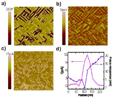
Thin films of BiFeO3 with thicknesses ranging between 40-70 nm have been slowly grown on SrRuO3-buffered SrTiO3 substrates, as described in ref.Dau10 . The as-grown samples contain monoclinic (pseudo-rhombohedral) crystallographic twin domains. From the eight possible twinsStr98 , only the four variants pointing towards the SrRuO3 electrode are present in the films, in agreement with other reportsJan09 . Most of the domain walls (dws) are 71o dws (where 71o is the approximate angular difference between the polarization vectors at both sides of the wall). In between two perpendicular sets of 71o dws, some 109o dws can also be foundDau10 . These ferroelectric/ferroelastic domains can be imaged by in-plane piezo-force microscopy (IP-PFM), using the metallic tip (Co-Cr coated Si) of an AFM microscope, as observed in Figure 1a)-b). The position and type of the dws can be accurately determined in this way. Simultaneously, the conduction through the sample, from the electrically grounded tip to the bottom SrRuO3 electrode (held at variable bias voltages), can be locally measured and mapped using a TUNATM amplifier (Bruker Corp.), which is designed to measure leakage currents from fA to A. One such map is reproduced in figure 1c) and, when compared to the IP-PFM images, it reveals that the 71o (as well as the 109o domain walls) in these films are conducting at room temperature, while the domains are not conducting at this temperature. Figure 1d) shows both the in-plane piezoelectric response and the current when scanning across a 71o domain wall, showing the maximum conductivity in the middle of the wall (characterized by the minimum piezoelectric response). This is different from what is observed in other BiFeO3 samples grown on DyScO3, substrates, at higher deposition rates and with higher oxygen pressure by Seidel et al.Sei09 . In this case, conduction was found only at 109o dws. Conduction at 71o dws is advantageous because of their larger stabilityRam11 ; Str98 .
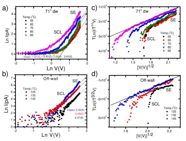
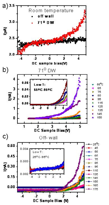
Figure 2a) displays I-V curves for the 71o dws and off-wall at room temperature in linear scale, showing the rectifying diode behavior of the domain walls, as previously reported for the 109o wallsSei09 . The forward diode direction coincides with that of the electrical polarization and it indicates that carriers are n-typeBlo94 ; Cho09 . In order to gain control on the currents, we investigate the conduction mechanisms by measuring the I-V curves at different temperatures (from 20 oC to 200 oC, in air). These curves are plotted in Figures 2b)-c) for 71o dws and off-wall, respectively. About 100 walls are investigated and all showed similar behavior. We have looked for signatures of interface-limited conduction, such as Fowler-Nordheim tunneling (ln(I/V2) E-1) or Richardson-Schottky-Simmons emission (lnI/(T3/2V) V1/2)Sim65 , as well as of bulk-limited Poole-Frenkel emission (ln(I/V) V1/2). The existence of current limitation due to built-in space charge (I V2) is also investigated.
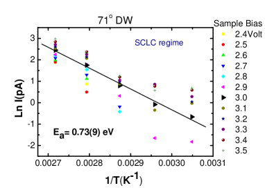
Interestingly, although appreciable conduction through the domains could only be observed at high temperatures (see figure 2), qualitatively similar behavior has been found for the two conduction paths (71o and off-wall) with two distinct regimes: For low voltages, conduction behaves like space-charge limited. This can be observed from the slope of the curves in figure 3a),b). The slope is around 2Note1 for voltages ranging from 1.5 V (where appreciable conduction starts) to about 3-3.5 V (depending of temperature). The temperature dependence in this regime shows Arrhenius thermal activation (see Figure 4). The activation energies extracted from the Arrhenius plots are consistent with defect states located 0.73(9)eV and 0.65(1)eV below the bottom of the conduction band, for 71o dws and off-wall, respectively. These values are too large for single electron traps at oxygen vacancies but they agree with those at clusters of oxygen vacancies in perovskites, and those reported for 109o domain wallsSei10 .
At large enough voltage (and temperatures), Schottky emission (SE) is observedSim65 , as it can be elucidated from the linear behavior in Figure 3c)-d). The axes in the plots are chosen such as to display the same slope for the different temperatures. The slopes are shown with solid lines. It can be seen that the higher the temperature, the larger the voltage range for which SE is observed, as expected for termionic emission. The barrier heights obtained from fitting the Richardson-Schottky-Simmons equationSim65 Note differ considerably between the domain walls and the domains, being 0.8(1)eV for the 71o dws and 2.6(7)eV inside the domains. This large difference explains the lower currents measured at the domains and its reduction at room temperature below the sensitivity limit of the TUNATM amplifier(5fA).
The Poole-Frenkel (PF) mechanism (field-assisted electron de-trapping) was also tested. The voltage dependence is similar to that of the SE, but the optical dielectric permittivity values obtained from the fits were considerably worse than those obtained from the SE equations. The dielectric permittivity at high frequencies in BiFeO3 in 6.25Pin05 ; a value of 6.5 1.5 was obtained for 71o dws using the slope indicated in Figure 3c). With the PF fits, the obtained permittivity value is 0.4 0.1. We observe then that the large currents (high voltage -high temperature) are interface-limited.
It is unusual that a space-charge-limited-like regime takes place at low currents. An explanation for this is provided by Blom et al.Blo94 : the ferroelectric surface charges themselves create a space-charge-like region giving rise to the I V2 dependence. At large positive bias and higher temperatures, the positively charged oxygen vacancies would be able to diffuse towards the top surface to neutralize the polarization surface charge, decreasing the space charge limitation and finally allowing Schottky emission of electrons from the tip. Support for this model is provided by samples grown at a higher oxygen pressure (300 mbar instead of 100 mbar). In this case, the ”space charge limited regime” (or more properly, the I V2 regime governed by the ferroelectric polarization) prevails up to the maximum measured bias (5V) for temperatures below 85o C and only above this temperature is an increase in the current observed. In this case, the behavior in the large temperature regime resembles that reported by Pintillie et al.Pin05 : Schottky emission with an unphysically small barrier of (0.14 eV, in our case) due to the influence of the ferroelectric polarization. This is indeed consistent with the fact that, in this sample with a lower number of oxygen vacancies present, the surface charges of the ferroelectric polarization are not completely neutralized by the oxygen vacancies.
The presence of n-type defect sates in the band gap (oxygen vacancies) will have two effects: first, to enable thermally activated electrons from defect state inside the band gap to be promoted to the conduction band, as discussed above, and second, the effect of reducing the Schottky barrier due to defect surface statesDaw01 . This second effect is critical to control conduction at domains and domain walls, since it determines the large current regime. The role of oxygen vacancies is, thus, direct only in the low current regime. In the large current regime (the interesting one for applications) the oxygen vacancies do not directly provide the carriers, but they lower the Schottky barrier more in the domains walls (0.8(1) eV) than in the domains (2.6 eV), probably due an accumulation of oxygen vacancies in the domain walls. The carriers are electrons injected from the conductive AFM tip. A large number of vacancies must be present in the films in order to avoid the current to be limited by the ferroelectric polarization.
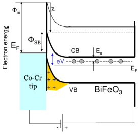
To conclude, we report that 71o, naturally-formed, ferroelastic domain walls of BiFeO3 grown on SrRuO3-buffered SrTiO3 provide well-defined conducting paths through the films, from the metallic tip acting as top electrode to the bottom SrRuO3 electrode. Conduction is provided by n-type carriers and the mechanisms for conduction are the same both at the domain walls and at the domains: the low current regime is supported by thermally activated electrons from defect (oxygen vacancies) states and limited by the ferroelectric polarization; the large current regime is regulated by Schottky emission from the tip. The observed differences in conduction between the domains and the walls are due to the different barrier heights at the interface with the metallic tip. The large currents are therefore interface-limited and can be controlled by engineering the the work function of the injection electrode and the defect density in the BiFeO3 layer.
References
- (1) E. Salje, H. L. Zhang, Phase Transitions 82, 452 (2009) and refs. therein ; E.K.H Salje, ChemPhysChem 11, 940 (2010) and refs. therein.
- (2) J. Privratska and V. Janovec Ferroelectrics 201, 321 (1997); Ferroelectrics 222, 33 (1999).
- (3) A.V. Goltsev, R.V. Pisarev, T. Lottermoser, and M. Fiebig, Phys. Rev. Lett. 90, 177204 (2003); T. Lottermoser and M. Fiebig, Phys. Rev. B 70, 220040 (2004).
- (4) M. Mostovoy, Phys. Rev. Lett. 96, 067601 (2006).
- (5) M. Daraktchiev, G. Catalan, and J.F. Scott, Phys. Rev. B 81, 224118 (2010).
- (6) C.J.M. Daumont, D. Mannix, S. Venkatesan, D. Rubi, G. Catalan, B.J. Kooi, J.Th.M. De Hosson, and B. Noheda, J. Phys.: Condens. Mat. 18, 182001 (2009); S. Venkatesan, C.J.M. Daumont, B.J. Kooi, B. Noheda, and J.Th.M. De Hosson, Phys. Rev. B 80, 214111 (2009).
- (7) L.W. Martin, Y.-H Chu, M.B. Holcomb, M. Huijben, P. Yu, S.J. Han, D. Lee, S.X. Wang, and R. Ramesh, Nanoletters 8, 2050 (2008).
- (8) J. Seidel, L.W. Martin, Q. He, Q. Zhan, Y.-H. Chu, A. Rother, M.E. Hawkridge, P. Maksymovych, P. Yu, M. Gajek, N. Balke, S.V. Kalinin, S. Gemming, F. Wang, G. Catalan, J.F. Scott, N.A. Spaldin, J. Orenstein, and R. Ramesh, Nat. Mat. 8, 229 (2009).
- (9) J. Seidel, P. Maksymovych, Y. Batra, A. Katan, S.-Y. Yang, Q. He, A. P. Baddorf, S.V. Kalinin, C.-H. Yang, J.-C. Yang, Y.-H. Chu, E. K. H. Salje, H. Wormeester, M. Salmeron, and R. Ramesh, Phys. Rev. Lett. 105, 197603 (2010)
- (10) H.W. Jang, D. Ortiz, S-H. Baek, C. M. Folkman, R. R. Das, P. Shafer, Y. Chen, C. T. Nelson, X. Pan, R. Ramesh, and C-B. Eom, Adv. Mater. 21, 817 (2009)
- (11) A. Vlooswijk, B. Noheda, G. Catalan, A. Janssens, B. Barcones, G. Rijnders, D.H.A. Blank, S. Venkatesan, B. Kooi, J.T.M. de Hosson, Appl. Phys. Lett. 91, 112901 (2007)
- (12) C.J.M. Daumont, S. Farokhipoor, A. Ferri, J. C. Wojdel, Jorge I iguez, B.J. Kooi and B.Noheda, Phys. Rev. B. (2010)
- (13) S.K. Streiffer, C. B Parker, A. E. Romanov, W. Pompe, C.M. Foster and G. R. Bai, J. of Applied Physics 83, 2742 (1998)
- (14) R. Ramesh (personal communication)
- (15) P.W.M. Blom, R.M. Wolf, J.F.M. Cillessen and M.P.C.M. Krijn, Phys. Rev. Lett. 73, 2107 (1994)
- (16) T. Choi, S. Lee,* Y. J. Choi, V. Kiryukhin, S.-W. Cheong, Science 324, 63 (2009).
- (17) J. G. Simmons, Phys. Rev. Lett. 15, 967 (1965)
- (18) It is worth to notice that these are local measurements using the AFM tip and that the electric field is highly inhomogeneous. A perfect quantitative agreement with the well-known conduction equations is thus not expected and our slope values of 1.8-2.8 can be considered in good agreement with the expected slope 2.
- (19) In this work we are assuming that the BiFeO3 is fully depleted and that the field at the interface (Eo) is proportional to the applied bias (V)Pin05 ; Zub06 .
- (20) P. Zubko, D. J. Yung and J.F. Scott, J. of Appl. Phys. 100, 114112 (2006); P. Zubko, D. J. Yung and J.F. Scott, J. of Appl. Phys. 100, 114113 (2006)
- (21) L. Pintilie, I. Boerasu, M. J. M. Gomes, T. Zhao, R. Ramesh, and M.Alexe, J. Appl. Phys. 98, 124104 (2005).
- (22) M. Dawber, J. Scott and A.J. Hartmann, J. of the Europ. Ceramic Soc. 21, 1633 (2001)