Interplay between interferences and electron-electron interactions in epitaxial graphene
Abstract
We separate localization and interaction effects in epitaxial graphene devices grown on the C-face of an 8-ooff 4H-SiC substrate by analyzing the low temperature conductivities. Weak localization and antilocalization are extracted at low magnetic fields, after elimination of a geometric magnetoresistance and subtraction of the magnetic field dependent Drude conductivity. The electron electron interaction correction is extracted at higher magnetic fields, where localization effects disappear. Both phenomena are weak but sizable and of the same order of magnitude. If compared to graphene on silicon dioxide, electron electron interaction on epitaxial graphene are not significantly reduced by the larger dielectric constant of the SiC substrate.
pacs:
72.20.My, 85.30.De, 72.80.EyI introduction
Graphene-based devices are exciting candidates for future generations of microelectronic devices. A promising technique to produce graphene at an industrial scale is the epitaxial graphene growth from a SiC substrate, because these SiC substrates can be patterned using standard lithography methods. Thanks to recent technical improvements, the most delicate and intrinsic features of graphene, those reflecting the chiral nature of the quasiparticles, as, for instance, the so-called ’Half Integer quantum Hall effect’ Shen et al. (2009); Jobst et al. (2010); Tzalenchuk et al. (2010); Wu et al. (2009) and the weak antilocalization Wu et al. (2007), have been recently reported for epitaxial graphene.
In graphene, depending on the relative magnitude of intervalley scattering time and phase coherence time, either weak localization (WL) or weak antilocalization (WAL) has been predicted Kechedzhi et al. (2007). The phase interference correction to the resistance depends on the nature of the disorder. For epitaxial graphene samples, elastic scattering favorable for WAL can be caused by remote charges like ionized impurities in the substrate. On the other hand, atomically sharp disorder (local defects, edges) causes intervalley scattering and gives rise to WL.
Experimentally, in two-dimensional gases, WL is often mixed with electron-electron interaction Altshuler et al. (1980) (EEI). As WL, EEI gives a correction to the Drude conductivity with a dependence. It follows that the experimental extraction and separation of EEI and WAL contributions are usually difficult Goh et al. (2008). For graphene, in the diffusive regime, EEI is expected to give this usual temperature dependence correction proportional to . EEI is also expected to be sensitive to the different kinds of disorders Kozikov et al. (2010).
In this work, we take advantage of simultaneous measurements of the longitudinal and transverse resistances to invert the resistivity tensor. We can then separate the different mechanisms which give corrections to the Drude conductivity: i) a geometric contribution, which experimentally appears as a constant term in the longitudinal conductivity; ii) WL and WAL, by a comparison between the experimental magnetoconductance and the Drude magnetoconductivity, iii) EEI, whose temperature dependence can be analyzed in the magnetic field range for which WAL has disappeared.
II Experimental details
We have used large and homogeneous single epitaxial graphene layers grown on the C-face of an insulating 8o off-axis 4H-SiC substrate. The graphene sheets have an elongated triangular shape of which quality and homogeneity can be easily checked using micro-Raman spectroscopy. On few selected samples, Cr/Au ohmic contacts were deposited to define Hall-bars with a rough geometry (see inset in Fig.1 for details). Then magneto-transport measurements were done using a 14T magnet in a cryostat and a Variable Temperature Inset operated down to 1.5K. On the best samples, at high magnetic field, the half-integer quantum Hall effect could be observed up to the last plateau in the temperature range 1.5 to 40K. For details, see Ref. Camara et al. (2010). In this work we focus on two moderately doped samples ( and ) with dimensions, carrier concentration, mobility and scattering times reported in table 1. We work at low injection currents (10nA- 1A), mainly at low magnetic fields ( 3T), low temperatures (1.5 K-200K) and we focus on the magnetic field dependence of the longitudinal and transverse elements of the resistivity tensor.
| sample | ||||||||
|---|---|---|---|---|---|---|---|---|
| 5 | 5 | 1.1 | 5000 | 0.57 | 0.1 | 0.065 | 0.03 | |
| 40 | 10 | 0.8 | 11000 | 0.48 | 0.15 | 0.11 | 0.057 |
III Background Considerations
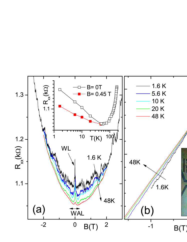
An overview of the results obtained for sample S1 is shown in Fig.1. The experimental longitudinal and transverse magnetoresistances and for sample are presented in Fig. 1a and 1b respectively, at different temperatures between 1.6K and 48K. Let us consider first, Fig. 1a. At low fields ( 0.1 T), a negative magnetoresistance peak centered at T is observed in . This peak is typical of weak localization (WL). Indeed, this peak a linear dependence of vs with a slope of the order of (see inset of Fig. 1a) and the amplitude of the peak is ( is the longitudinal resistivity). At higher magnetic fields, reproducible fluctuations in the conductance are also observed, with amplitudes for and for .
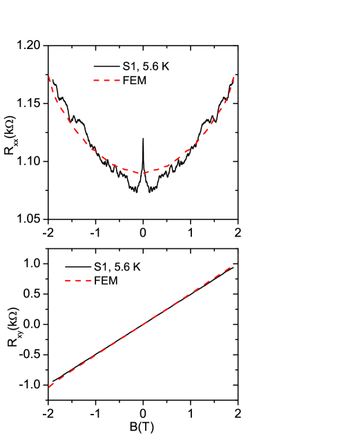
At magnetic fields T, a smooth depression is observed in , which we attribute to weak antilocalization (WAL). Because this WAL is barely visible in Fig. 1a, we also present additional experimental results in Appendix A. Experimentally, WAL is blurred because fluctuations of conductance are also present, and also because the positive magnetoresistance of the WAL is superposed to another positive magnetoresistance with a pronounced parabolic dependence, which is well observed on the whole magnetic field range T presented in Fig. 1a. The theory of weak localization is based on the diffusion approximation and does not hold for magnetic fields much higher than = 100 mT, where is the transport relaxation time and the diffusion coefficient. This means that the parabolic background above should not be attributed to WL features. It must have a different origin. Since the device is being far from having the shape of an ideal Hall-bar (see inset in Fig.1b) we ascribe this parabolic magnetoresistance component to magnetic deflection of the current lines. This is because the lateral probes are invasive and because the graphene layer under the lateral contacts is likely to have different mobility and carrier concentration Huard et al. (2008). For details, see Annex B.
Beyond geometric and interference corrections, a third correction to the resistivity manifests. It comes from electron-electron interactions and shows as: i) the persistence of a linear temperature dependence of , in a magnetic field range where interference effects are suppressed (see inset of Fig. 1a for a field of ); ii) a variation of the Hall slope (Fig. 1b) as a function of , which cannot be explained by variations of the carrier density, as the hole gas is strongly degenerate ( 20 for K, where is the Fermi energy); iii) a crossing of all resistances taken at different temperatures at (Fig. 1a) Minkov et al. (2001).
The justification of the last two points, originally given in Minkov et al. (2001), is as follows. EEI give no correction to the transverse conductance . It gives a small correction to the longitudinal conductance . This correction does not depend on if the magnetic field is smaller than a critical field . This condition if fulfilled for all the temperature and magnetic field ranges of this study. Because of this correction, EEI gives rise to a negative magnetoresistance in the first order in :
| (1) |
and a variation of the Hall slope where is the conductivity at . These relations are derived by inverting the conductivity tensor:
| (2) | |||
| (3) |
It has been established recently Goh et al. (2008) that the separation of EEI and WL Goh et al. (2008) is simplified if the magnetoconductivities and are used, rather than the resistivities. As already stressed, the conductivity of the graphene layer is different below the Cr/Au contacts and, strictly speaking, inverting the resistivity tensor is incorrect because the device is inhomogeneous. However, experimentally, the geometric correction is small, appears only in the longitudinal magnetoresistance as a parabolic correction, and consequently geometric corrections to the longitudinal conductivity appear as a -independent shift .
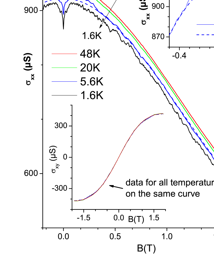
The magnetoconductivities for sample are plotted in Fig. 2 at different temperatures. The conductivities have been obtained from Eq. 2 and 3, where the resistivities have been estimated by and . The lower inset of Fig.2 shows that all taken at different temperatures collapse on the same curve, as expected for EEI. This also confirms that both mobility and carrier concentration are constant over the whole temperature range and, as the geometric correction only depends on via the Hall angle , that does not depend on the temperature. Finally, the -independence of the transverse conductivity indicates an effective separation of EEI () and interference () corrections over almost the whole -range. At low fields , a -dependence of due to WL is expected but is not observed, being beyond our experimental resolution.
The large decrease of between 0 and 2T in Fig. 2 is due to the magnetic field dependence of the Drude conductivity . We express the total conductivity by
| (4) |
When WL is negligible: , we impose and Eq. 4, for a given temperature, simplifies as , where is a constant which incorporates both geometric and EEI corrections. This last formula gives very good fits to the conductivity at all temperatures. As an example, the blue dotted line in Fig. 2 is the fit for the =5.6K data in the interval 0.5-2 T, where , and are the fit parameters. Transverse and longitudinal resistivities can be fitted separately but still give very similar mobilities and concentrations, which are reported in Table I.
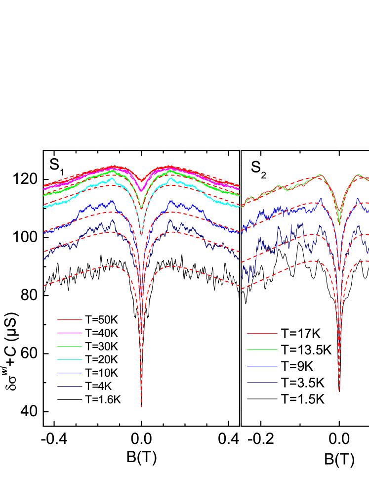
The upper inset in Fig. 2 is an enlargement of the low- data at and evidences the weak antilocalization peak which takes place around the weak localization centered at . A similar weak antilocalization can be detected for all temperatures. The WL theory does not take into account the modification of the current paths due to magnetic field. In other words, before examining the WL contribution to the conductivity, we should first subtract the Drude fits (given by the dotted line in Fig. 2) to the observed longitudinal conductivities Proskuryakov et al. (2001). Experimental results for samples and are shown in Fig. 3, for different temperatures.
IV Correction due to Weak localization and antilocalization
In the diffusive regime in graphene, is given by Kechedzhi et al. (2007):
| (5) |
where , is the digamma function, and are the coherence time, the intervalley scattering time and the intravalley scattering time respectively. For simplicity, we identify intervalley to short range (sr) scattering and intravalley to long-range (lr) scattering. We take constant scattering times and over the whole temperature range and only is allowed to depend on . Neglecting the warping Chen et al. (2010), we also impose . We then fit the conductivities at different temperatures by Eq. IV. Results are indicated by dashed lines in Fig. 3 (for sake of clarity, fits at high temperatures have not been reported). Best fit is obtained with the values reported in Table I. We estimate the short-range scattering length 100-140 nm. The long-range scattering length 70-90 nm is even shorter. These lengths are comparable to what is found in exfoliated graphene on SiO2 substrate Tikhonenko et al. (2008). They are also comparable to the distance between the SiC steps below the graphene layer. It is often stated that exfoliated graphene is much more disordered at the edge of the SiC steps Jouault et al. (2010). Therefore step edges could be the main source of scatterings in these samples.
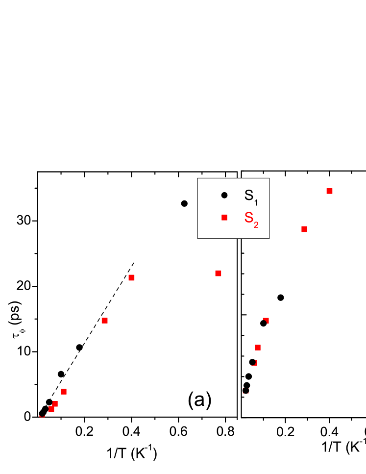
The phase coherence time obtained from the fit is plotted in Fig. 4. Apart from a saturation at low , is roughly proportional to between 10K-50K with a slope equal to 50 ps K for samples and . We conclude that obeys the usual temperature dependence for electron electron scattering in the diffusive regime:
| (6) |
where is the reduced conductivity: and the empirical coefficient is 1 for and 1.4 for . Similar observations have already been done both for epitaxial Wu et al. (2007) and exfoliated graphene Tikhonenko et al. (2008); Morozov et al. (2006). The coherence length is readily calculated and plotted in fig. 4b. At low temperature, slightly exceeds 1m.
V Correction due to Electron Electron Interaction
We attribute the temperature dependence of the conductivity to EEI. The Drude mobility is constant over the whole temperature range, therefore there is no temperature dependence of the conductivity induced by electron-phonon scattering. This is not surprising, as the temperature dependence for graphene is small below the Grüneisen temperature given by 54 K, where the concentration is in unit of 1012cm-2 Stauber et al. (2007); Hwang and Das Sarma (2008). For our samples, 54 K, and almost all our measurements are done below the Grüneisen temperature.
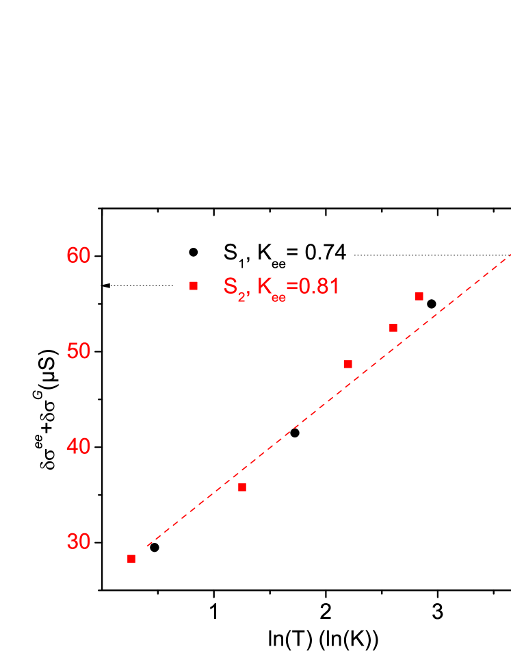
As , we are by definition in the diffusive regime, for which EEI theory predicts a temperature dependent correction to the conductivity given by:
| (7) |
where is a prefactor whose value depends on the different channels contributing to the EEI Kozikov et al. (2010). In fig. 5, we show for samples and . The expected dependence is evidenced and the slope gives = 0.81 and 0.74 for samples and respectively. These values are very similar to recent experimental findings on exfoliated graphene Kozikov et al. (2010); Moser et al. (2010). In a 2D system with a single valley, takes the form Klimov et al. (2008)
| (8) |
where the unity represents the so-called ’charge’ contribution (the Fock and singlet part of Hartree term), the prefactor is the number of ’triplet’ channels (from the Hartree term) and is the liquid Fermi constant. At low temperatures ( 15 K for and for ), when long range and short range scattering rates are important, the usual single-valley case is recovered with a prefactor . This leads to = -0.13 . This value is small and very close to the value of recently found for exfoliated graphene Kozikov et al. (2010). This is somehow surprising, as the dielectric constant in SiC (10) is larger than in SiO2 (3.9) and we would expect even smaller electron-electron interactions because of the screening of the substrate. However, numerical estimation of following, for instance, Ref. Kozikov et al. (2010) gives : a value compatible with our experiment. Also, Ref. Polini et al. (2007) predicts values for the Fermi liquid constant only slightly smaller than our findings. Interestingly, it was also recently quoted Kozikov et al. (2010) that at intermediate temperatures , additional triplet channels originating from pseudospin conservation (ie valley degeneracy) become relevant and the number of triplet channels increases to . However, we do not observe any change in the slope in Fig. 5 from =1.5K up to 50K. The situation is similar in Ref. Moser et al. (2010), where EEI is observed on a temperature range on which the slope should vary, but where experimentally the slope remains constant.
To conclude, we show, beyond classical geometric corrections, weak localization, weak antilocalization and electron-electron interactions in epitaxial graphene. Weak antilocalization is observable directly in the resistances, and its analysis gives access to the different scattering times, which are very close to those for exfoliated graphene on SiO2 substrates. Electron-electron interaction gives also a small correction to the conductivity, which is not significantly smaller than in exfoliated graphene.
We acknowledge the EC for partial support through the RTN ManSiC Project, the French ANR for partial support through the Project Blanc GraphSiC and the Spanish Government for a grant Juan de la Cierva. N. C. also acknowledges A. Bachtold’s, A. Barreiro and J. Moser from ICN Barcelona, for technical and theoretical supports.
beginthebibliography22
References
- Shen et al. (2009) T. Shen, J. J. Gu, M. Xu, Y. Q. Wu, M. L. Bolen, M. A. Capano, L. W. Engel, and P. D. Ye, Applied Physics Letters 95, 172105 (2009).
- Jobst et al. (2010) J. Jobst, D. Waldmann, F. Speck, R. Hirner, D. K. Maude, T. Seyller, and H. B. Weber, Phys. Rev. B 81, 195434 (2010).
- Tzalenchuk et al. (2010) A. Tzalenchuk, S. Lara-Avila, A. Kalaboukhov, S. Paolillo, M. Syvajarvi, R. Yakimova, O. Kazakova, T. J. B. M. Janssen, V. Fal’ko, and S. Kubatkin, Nature Nano. 5, 186 (2010).
- Wu et al. (2009) X. Wu, Y. Hu, M. Ruan, N. K. Madiomanana, J. Hankinson, M. Sprinkle, C. Berger, and W. A. de Heer, Applied Physics Letters 95, 223108 (2009).
- Wu et al. (2007) X. Wu, X. Li, Z. Song, C. Berger, and W. A. de Heer, Phys. Rev. Lett. 98, 136801 (2007).
- Kechedzhi et al. (2007) K. Kechedzhi, E. McCann, H. Suzuura, and B. Altshuler, Eur. Phys. J. Special Topics 148, 39 (2007).
- Altshuler et al. (1980) B. L. Altshuler, A. G. Aronov, and P. A. Lee, Phys. Rev. Lett. 44, 1288 (1980).
- Goh et al. (2008) K. E. J. Goh, M. Y. Simmons, and A. R. Hamilton, Phys. Rev. B 77, 235410 (2008).
- Kozikov et al. (2010) A. A. Kozikov, A. K. Savchenko, B. N. Narozhny, and A. V. Shytov, Phys. Rev. B 82, 075424 (2010).
- Camara et al. (2010) N. Camara, B. Jouault, A. Caboni, B. Jabakhanji, W. Desrat, E. Pausas, C. Consejo, N. Mestres, P. Godignon, and J. Camassel, Applied Physics Letters 97, 093107 (2010).
- Huard et al. (2008) B. Huard, N. Stander, J. A. Sulpizio, and D. Goldhaber-Gordon, Phys. Rev. B 78, 121402 (2008).
- Minkov et al. (2001) G. M. Minkov, O. E. Rut, A. V. Germanenko, A. A. Sherstobitov, V. I. Shashkin, O. I. Khrykin, and V. M. Daniltsev, Phys. Rev. B 64, 235327 (2001).
- Proskuryakov et al. (2001) Y. Y. Proskuryakov, A. K. Savchenko, S. S. Safonov, M. Pepper, M. Y. Simmons, and D. A. Ritchie, Phys. Rev. Lett. 86, 4895 (2001).
- Chen et al. (2010) Y.-F. Chen, M.-H. Bae, C. Chialvo, T. Dirks, A. Bezryadin, and N. Mason, Journal of Physics: Condensed Matter 22, 205301 (2010), URL http://stacks.iop.org/0953-8984/22/i=20/a=205301.
- Tikhonenko et al. (2008) F. V. Tikhonenko, D. W. Horsell, R. V. Gorbachev, and A. K. Savchenko, Phys. Rev. Lett. 100, 056802 (2008).
- Jouault et al. (2010) B. Jouault, B. Jabakhanji, N. Camara, W. Desrat, A. Tiberj, J.-R. Huntzinger, C. Consejo, A. Caboni, P. Godignon, Y. Kopelevich, et al., Phys. Rev. B 82, 085438 (2010).
- Morozov et al. (2006) S. V. Morozov, K. S. Novoselov, M. I. Katsnelson, F. Schedin, L. A. Ponomarenko, D. Jiang, and A. K. Geim, Phys. Rev. Lett. 97, 016801 (2006).
- Stauber et al. (2007) T. Stauber, N. M. R. Peres, and F. Guinea, Phys. Rev. B 76, 205423 (2007).
- Hwang and Das Sarma (2008) E. H. Hwang and S. Das Sarma, Phys. Rev. B 77, 115449 (2008).
- Moser et al. (2010) J. Moser, H. Tao, S. Roche, F. Alzina, C. M. Sotomayor Torres, and A. Bachtold, Phys. Rev. B 81, 205445 (2010).
- Klimov et al. (2008) N. N. Klimov, D. A. Knyazev, O. E. Omel’yanovskii, V. M. Pudalov, H. Kojima, and M. E. Gershenson, Phys. Rev. B 78, 195308 (2008).
- Polini et al. (2007) M. Polini, R. Asgari, Y. Barlas, T. Pereg-Barnea, and A. MacDonald, Solid State Communications 143, 58 (2007), ISSN 0038-1098, exploring graphene - Recent research advances, URL http://www.sciencedirect.com/science/article/B6TVW-4NKXWM7-6/%2/79999e036e174b9401e32c27d650fe55.
VI Appendix A
In Fig. 6, we present magnetoresistances of samples , and of an additional monolayer , more doped. A straight line has been subtracted for sample , for clarity. For all three samples, a dip is observed on the two sides of the central WL peak. We attribute the dip to WAL.

VII Appendix B
We suggest that most part of the parasitic magnetoresistance comes from the invasive lateral probes. In order to sustain this assumption, classical magnetoresistances can be calculated by means of finite elements method (FEM) for the geometry of the devices. The simplest model only assumes different concentration and mobility under the lateral probes, and the results of this model are shown in Fig. 7 for sample . There is a good agreement with the experiment for a reduced mobility and an increased concentration under the probes, which seems reasonable if these region have been damaged during the electron beam lithography.