Diluted magnetic semiconductor heterostructure AlSb/InAs/ZnMnTe
with
giant Zeeman effect for two dimensional electrons in InAs
Abstract
A new approach to the growth of diluted magnetic semiconductors with two dimensional electron gas in InAs quantum well has been developed. The method is based on molecular-beam epitaxy of coherent “hybrid” AlSb/InAs/(Zn,Mn)Te heterostructures with a III-V/II-VI interface inside. The giant Zeeman splitting of the InAs conduction band caused by exchange interaction with Mn2+ ions has been proved by measuring the microwave radiation induced spin polarized electric currents.
pacs:
72.25.Fe, 73.21.Fg, 73.63.Hs, 78.67.DeThe concept of spin-based electronics demands semiconductor heterostructures possessing high electron mobility, pronounced ferromagnetic properties and strong spin-orbit interaction (SOI).Dietl_Spintronics ; Dyakonov_book In particular, manganese doped diluted magnetic semiconductors (DMS) showing high Curie temperature and large Landé factor are in the focus of current research. While enhanced magnetic properties have been obtained in (Cd,MnTe)- (Ga,Mn)As-based heterostuctures, the SOI in these materials is rather small. Thus, realization of low-dimensional DMS structures based on materials which possess a strong SOI, e.g. InAs, becomes important. Most recently it has been demonstrated that the incorporation of Mn into a heterostructure device containing an InAlAs/InGaAs quantum well (QW) leads to a two-dimensional hole gas. Wurstbauer_2009 In these structures the Mn ions are in close proximity to the InGaAs channel hosting the hole gas. While DMS hole systems with strong SOI have been realized and demonstrate very interesting magnetotransport properties, Wurstbauer_2010 the fabrication of InAs-based DMS with two-dimensional electron gas (2DEG) channels has been a challenge up until now. The 2DEG is characterized by a simple parabolic band structure and much higher mobility compared to that of the holes, even in Mn-doped DMS structures like (Cd,Mn)Te QW; Furdyna_1988 features making 2DEG systems attractive for various applications.
Here we introduce a novel concept to grow Mn modulation doped DMS structures with an InAs 2DEG channel. The structures were fabricated by means of molecular-beam epitaxy (MBE) growth of III-V/II-VI “hybrid” heterostructures with the InAs QW following the recipes given in Ref. Ivanov_2004_1, . The Mn layers have been inserted into the II-VI barrier at distance of 10 monolayers (ML) from InAs QW which is smaller than the magnetic length of 2D electrons. To explore the magnetic properties of the 2DEG we investigated spin polarized electric currents induced by microwave (mw) radiation.Ganichev_2009 ; Drexler_2010 Our measurements show that hybrid AlSb/InAs/(Zn,Mn)Te QW are characterized by enhanced magnetic properties which can be changed by tuning of the spatial position of Mn-doping layer as well as by the variation of temperature.

The structures were grown on (001)-oriented GaAs semiinsulating substrates at temperature of 280 ∘C. For the fabrication of AlSb/InAs/(Zn,Mn)Te heterovalent heterostructures with different designs of Mn-containing barrier we used two separated MBE setups. The first MBE (Riber 32P, France) was employed to obtain the III-V part consisting of the 0.2 m-thick GaAs and 2 m-thick GaSb buffer layers capped with a 4 nm-thick AlSb barrier and a 15 nm-thick InAs QW (two last layers have common InSb-like interface). A (2.5 nm-GaSb/2.5 nm-AlSb)10 superlattice was placed within the first third of the GaSb buffer to suppress propagation of misfit-induced threading dislocations. The II-VI parts of the heterovalent structures were deposited pseudomorphically on the III-V part in the second two-chambers MBE setup (Semiteq, Russia) after the ex-situ sulfur chemical passivation in a 1M NaO solution of the top InAs layer. The coherent growth of ZnTe on InAs was initiated by simultaneous opening of Zn and Te fluxes onto a (2x4)As-reconstructured InAs surface annealed preliminary under an As4 flux in the III-Arsenide chamber of the Semiteq’s setup and transferred to the II-VI chamber through ultrahigh vacuum. Such technology results in a high quality coherent AlSb/InAs/ZnTe QW structures demonstrating the existence of a 2DEG and quantum confined photoluminescence.Ivanov_2004_2 According to X-ray photoelectron spectroscopy studies of the InAs/ZnTe heterovalent interface grown under similar conditions, its conduction band offset (1.65 eV, see Ref. Gleim_2002, ) is close to that for InAs/AlSb interface. As a result we obtain AlSb/InAs/ZnTe QW nearly symmetric for electrons but strongly asymmetric for holes, which facilitates hole escape to the Sb-based barriers even if some acceptors are introduced into the QW.
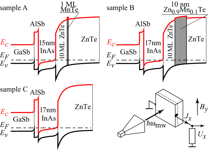
To demonstrate that the incorporation of Mn leads to enhanced magnetic properties of InAs 2DEG we prepared two samples with MnTe insertions (samples #A and #B) and one reference structure of the same design but without Mn (#C). The structures have similar composition but differ essentially in the design of the II-VI barrier grown on top of the QW, as shown in Fig. 1. In sample A we used 1 ML thick MnTe insertion separated from the InAs QW by 10 ML of non-magnetic ZnTe. Sample B has the same spacer, but in this structure instead of 1 ML of MnTe we have grown a 10 nm of Zn0.9Mn0.1Te with substantially smaller concentration of Mn per ML. In the last reference sample C no Mn atoms have been added and the II-VI barrier comprises ZnTe only.
The 2DEG has the density 11013 cm-2 and the mobility 103 cm2/Vs at a temperature K. In all investigated magnetic and non-magnetic samples mobilities are almost equal and much smaller than that in the AlSb/InAs/AlSb QW of conventional design. This fact indicates that the electron transport in hybrid structures is governed mostly by the InAs/ZnTe interface, which seem to involve fluctuating electrical dipoles due to inhomogeneous distribution of In-Te and Zn-As bonds and scattering centers of various origin, while the scattering by Mn atoms is negligible.
The setup used for the measurements of the mw-induced current is shown in Fig. 1. To heat the 2DEG we applied linearly polarized microwave radiation of a backwardwave oscillator (BWO) operating at frequency of 290 GHz or a Gunn diode with GHz. The incident mw power, , of about 2 mW was modulated at 330 Hz by means of a chopper or using a switch for the BWO and Gunn diode, respectively. Unbiased samples of 55 mm2 with a pair of Ohmic contacts centered along opposite edges were irradiated by mw radiation at normal incidence. The resulted photocurrent ( [10]) was measured via the voltage drop across a 1 M load resistor applying lock-in technique.

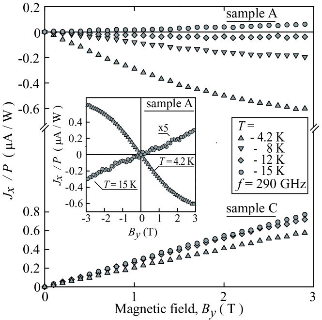
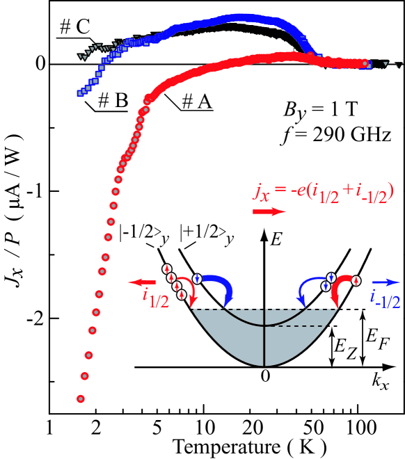
Figure 2 shows the magnetic field dependence of the photocurrent induced in samples A and C. The current increases with and reverses its sign as the direction of changes (see inset in Fig. 2). The temperature dependence of for all samples is plotted in Fig. 3. Both figures indicate a remarkable difference in the photocurrents generated in Mn-doped samples A and B and the reference sample C. At temperatures above 60 K the current in all three structures has the same sign and nearly the same magnitude. The analogy, however, disappears as the temperature decreases. In the reference sample C the polarity of the signal and its magnetic field behavior remains unchanged. By contrast, in structures doped with Mn a reduction of temperature results in a sign inversion of the current at . The most remarkable behavior is detected in sample A with K. In this sample below the current increases by more than one order of magnitude compared to that measured in samples B and C at the same temperature. We also observed that in this sample for K the photocurrent does not depend linearly on anymore, and saturates at high magnetic fields (see Fig. 2). In sample B the inversion temperature is substantially lower ( K) and the signal is much smaller than that in sample A.
All these findings give a strong evidence for enhanced magnetic properties of the Mn-doped structures and can be well understood in the frame of the recently proposed model for the spin-dependent asymmetric energy relaxation of a nonequilibrium 2DEG. Ganichev_2009 ; Drexler_2010 The inset in Fig. 3 sketches the basic physics of this phenomenon. Excitation of the 2DEG by mw radiation causes electron gas heating. In InAs QWs the spin-dependent electron-phonon interaction in the energy relaxation results in equal and oppositely directed electron fluxes, , for opposite spin subbands, . The application of the magnetic field emerges a Zeeman splitting. Thus, the electron densities in the subbands become different, and the fluxes do not compensate each other yielding a net electric current . Obviously, the current is spin polarized and its value is proportional to the Zeeman splitting energy .

The coupling of the photocurrent sign and magnitude to the band spin splitting results in a different behavior of in sample C and Mn-doped samples A and B. In the non-magnetic structure (for bulk InAs , see Ref. Madelung_1982, ). Consequently, the current increases linearly with rising magnetic field and does not change its sign upon variation of temperature. For the Mn-doped samples a strong temperature dependence of the band spin splitting as well as reversing its sign upon temperature variation is expected if 2D electrons are coupled to Mn2+ ions. These effects are well known for 2DEG in (Cd,Mn)Te/(Cd,Mg)Te DMS structures where the band spin splitting in DMS QWs is given by Furdyna_1988
| (1) |
Here is the Boltzmann constant, the Bohr magneton, is Mn -factor, is the Mn-spin system temperature, parameters and account for the Mn-Mn antiferromagnetic interaction, is the Mn concentration, is the modified Brillouin function, and is the exchange integral. It is seen that the Zeeman splitting in DMS structures differs from that in the non-magnetic material by the second term which is caused by electron exchange interaction with the Mn2+ ions. Equation (1) explains well the experimental data for our Mn-doped structures. The effect of the exchange interaction is most pronounced at low temperatures at which the last term in Eq. (1) causes the giant Zeeman spin splitting. The current is proportional to . Following the it is drastically enhanced and saturates at high magnetic fields (see Fig. 2). With the temperature increase, the role of the exchange interaction decreases, diminishes, and, for a certain temperature, the intrinsic band spin splitting becomes dominant. Due to the opposite signs of * and the sign of inverses resulting in the reversion of the photocurrent direction (see Fig. 3).footnote1 Lower inversion temperature and substantially smaller magnitude of the current detected in sample B in comparison to that of sample A indicate the weaker influence of Mn on the magnetic properties of the InAs 2DEG channel in this sample.
Our data unambiguously demonstrate that Mn2+ ions crucially affect the magnetic properties of the InAs 2DEG channel. In both magnetic samples the Mn doping is done after the InAs QW growth (Fig. 1) and is separated from the QW by rather thick spacer of ZnTe (10 ML), so that the InAs channel is expected to be free of manganese.Wurstbauer_2009 ; Prechtl_2003 The latter is also in agreement with the transport data, because diffusion of Mn into the InAs channel should yield a hole gas rather then 2DEG. Thus, we attribute the effect of magnetic ions to the exchange interaction caused by the penetration of electronic wave function into the barrier.Meilikhov_2010 The observed weaker magnetic properties in sample B comparing to sample A supports this mechanism. In both samples we used Mn insertions with almost the same number of Mn atoms placed after the 10 ML spacer for which the magnetic length of 2D electrons remains larger than the spacer in the whole range of magnetic fields used here. The only difference is that in sample A the doping with magnetic ions is localized in 1 ML and in sample B it is distributed over a larger distance of 10 nm. Thus, the electron wave function has better overlap with Mn ions in sample A compared to sample B resulting in increased exchange interaction and more pronounced magnetic properties.
Summarizing, we show that a structures characterized by a giant Zeeman splitting in -type InAs QW and showing behavior typical for DMS can be obtained by growing of III-V/II-Mn-VI coherent “hybrid” heterostructures with the Mn insertion to the II-VI barrier. Our measurements demonstrate that enhanced magnetic properties are due to penetration of electronic wave function into the (Zn,Mn)Te layer and can be controllably varied by the position and density of Mn2+ ions.
The financial support from the DFG (SFB 689 and Priority Group 1483), the Linkage Grant of IB of BMBF at DLR, RFBR and Russian Ministry of Education and Sciences is gratefully acknowledged. We are grateful to B. Aronzon and D. Yakovlev for fruitful discussions.
References
- (1) Spintronics in Semiconductors and Semimetals series, T. Dietl, D. Awschalom, and M. Kaminska eds. (Academic Press, London, 2008).
- (2) Spin Physics in Semiconductors, M. I. Dyakonov ed. (Berlin, Springer, 2009).
- (3) U. Wurstbauer et al., J. Cryst. Growth 311, 2160 (2009).
- (4) U. Wurstbauer et al., Nature Phys. 6, 955 (2010).
- (5) J. K. Furdyna, J. Appl. Phys. 64, R29 (1988).
- (6) S. V. Ivanov et al., phys. stat. sol. (c) 1, 1468 (2004).
- (7) S. D. Ganichev et al., Phys. Rev. Lett. 102, 156602 (2009).
- (8) C. Drexler et al., Appl. Phys. Lett. 97, 182107 (2010).
- (9) S. V. Ivanov et al., Appl. Phys. Lett., 84, 4777 (2004).
- (10) Th. Gleim et al., Appl. Phys. Lett. 81, 3813 (2002).
- (11) O. Madelung, M. Schulz, and H. Weiss, Landolt-Börnstein, New Series, Group III, Part 17a (Springer, 1982).
- (12) We note, that a similar ( behavior has also been observed recently in (Cd,Mn)Te/(Cd,Mg)Te QWs where, in contrast to the structures studied here, (Cd,Mn)Te thin layers were directly implemented in the QW.
- (13) G. Prechtl et al., Phys. Rev. B 68, 165313 (2003).
- (14) E. Z. Meilikhov and R. M. Farzetdinova, JETP 110, 794 (2010).