Transport properties of graphene quantum dots
Abstract
In this work we present a theoretical study of transport properties of a double crossbar junction composed by segments of graphene ribbons with different widths forming a graphene quantum dot structure. The systems are described by a single-band tight binding Hamiltonian and the Green’s function formalism using real space renormalization techniques. We show calculations of the local density of states, linear conductance and I-V characteristics. Our results depict a resonant behavior of the conductance in the quantum dot structures which can be controlled by changing geometrical parameters such as the nanoribbon segments widths and relative distance between them. By applying a gate voltage on determined regions of the structure, it is possible to modulate the transport response of the systems. We show that negative differential resistance can be obtained for low values of gate and bias voltages applied.
pacs:
61.46.-w, 73.22.-f, 73.63.-bI Introduction
In the last few years, graphene-based systems have attracted a lot of scientific attention. Graphene is a single layer of carbon atoms arranged in a two dimensional hexagonal lattice. In the literature, it has been reported several experimental techniques in order to obtain this crystal, such as mechanical peeling or epitaxial growthNovoselov ; berger1 ; berger2 . On the other hand, graphene nanoribbons (GNRs) are stripes of graphene which can be obtained by different methods like high-resolution lithography chinos , controlled cutting processesCi or by unzipping multiwalled carbon nanotubes Kosynkin . Different graphene heterostructures based on patterned GNRs have been proposed and constructed, such as graphene junctions jarillo , graphene flakes ponomarenko , graphene antidots superlattices pedersen , and graphene nano-constrictions jarillo2 . The electronic and transport properties of these nanostructures are strongly dependent of their geometric confinement, allowing the possibility to observe quantum phenomena like quantum interference effects, resonant tunneling and localization. In this sense, the controlled modification of these quantum effects by means of external potentials which change the electronic confinement, could be used to develop new technological applications such as graphene-based composite materials stankovic , molecular sensor devices schedin ; Rosales and nanotransistors Stampfer .
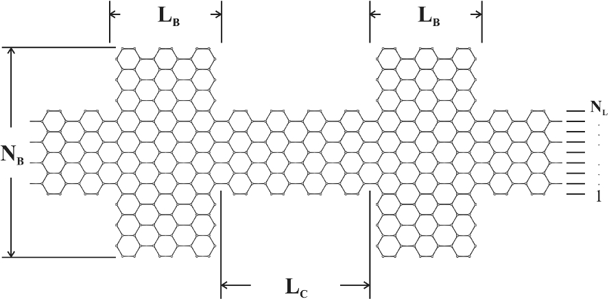
In this work we study the transport properties of quantum-dot like structures, formed by segments of graphene ribbons with different widths connected between each other, forming a double crossbar junctionGonzalez ; chinos2 . These graphene quantum dots (GQDs) could be versatile experimental systems which allow a range of operational regimes from conventional single-electron detectors to ballistic transport. The systems we have considered are conductors formed by two symmetric crossbar junctions of widths and length , and a central region that separates the junctions, of width and length . Two semi-infinite leads of width are connected to the ends of the central conductor. A schematic view of the considered system is presented in figure 1. We studied the different electronic states appearing in the system as a function of the geometrical parameters of the GQD structure. We found that the GQD local density of states (LDOS) as a function of the energy shows the presence of a variety of sharp peaks corresponding to localized states and also states that contributes to the electronic transmission which are manifested as resonances in the linear conductance. By changing the geometrical parameters of the structure, it is possible to control the number and position of these resonances as a function of the Fermi energy. On the other hand a gate voltage applied at selected regions of the conductor allows the modulation of their transport properties exhibiting a negative differential conductance (NDC) at low values of the bias voltage.
II Model
All considered systems have been described by using a single -band tight binding hamiltonian, taking into account nearest neighbor interactions with a hopping parameter . Besides, we have considered hydrogen passivation by setting a different hopping parameter for the carbon dimers at the ribbons edgesSon , .
The electronic properties of the systems have been calculated using the surface Green’s functions matching formalism (SGFMF)Nardelli ; Rosales . In this scheme, we divide the heterostructure in three parts, two leads composed by semi-infinite pristine GNRs, and the conductor region composed by the double GNRs crossbar junctions, as it is shown in figure 1.
In the linear response approach, the electronic conductance is calculated by the Landauer formula. In terms of the conductor Green’s functions, it can be written asDatta :
| (1) |
where , is the transmission function of an electron crossing the conductor region, is the coupling between the conductor and the respective leads, given in terms of the self-energy of each lead: . Here, are the coupling matrix elements and is the surface Green’s function of the corresponding lead Rosales . The retarded (advanced) conductor Green’s function are determined byDatta :
| (2) |
where is the hamiltonian of the conductor. In order to calculate the differential conductance of the systems, we determine the I-V characteristics by using the Landauer formalismDatta . At zero temperature, it reads
| (3) |
where is the chemical potential of the system in equilibrium and is defined by equation (1). The Green’s functions and the coupling terms depend on the energy and the bias voltage. We consider a linear voltage drop along the longitudinal direction of the conductor and the gate voltage is included in the on-site energy at the regions in which this potential is applied. In what follows the Fermi energy is taken as the zero energy level, all energies are written in terms of the hopping parameter and the conductance is written in units of the quantum of conductance .
III Results and discussion
In figure 2, we display results of the linear conductance for a graphene quantum dot structure formed by two armchair ribbons leads of width and a conductor region composed by two symmetric crossbar junctions of width and variable lengths (from up to ) . Two relative distances between the junctions: panel (a) and panel (b) are considered and the conductance of a pristine armchair nanoribbon is included as a comparison (light green dotted line).
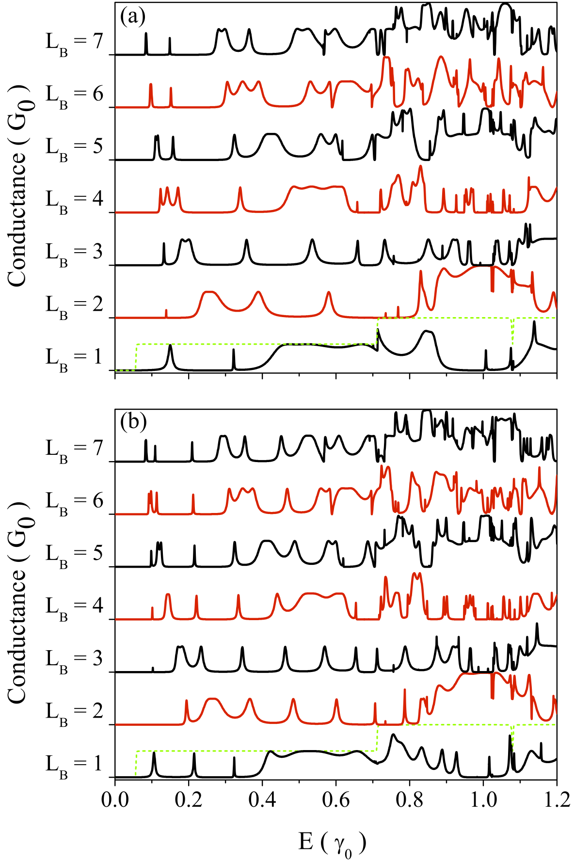
In both panels it is possible to observe a series of peaks at defined energies in the conductance curves. This resonant behavior of the electronic conductance arises from the interference of the electronic wave functions inside the structure, which travel forth and back forming stationary states in the conductor region (well-like states). In order to understand these results, it is convenient to define two energy regions, the low-energy range from up to (corresponding to the first quantum of conductance for the pristine armchair ribbon) and the high-energy range, from to (corresponding to the second step of conductance of the pristine system).
In the low-energy range, it is clear that the conductance peaks correspond to resonant states belonging to the central region of the conductor. By increasing the relative distance of the central part of the system, the number of allowed well-like states also increases and, as a consequence, the conductance curves exhibit more resonancesRosales ; Gonzalez ; Zhang . The well-like states remain almost invariant under geometrical modifications of the crossbar junctions. However, for certain energy ranges and for particular junction lengths, the electronic transmission of the systems. exhibits an almost constant value. For instance, in both panels of figure 2, for the cases of and at the energy range 0.4 to 0.65 . This effect corresponds to a constructive interference between well-like states from the central region with states belonging to the crossbar junctions regions. The different interference effects will be clarified by analyzing the LDOS of these systems, which is shown next in this paper. In the high-energy region, the conductance curves exhibit a complex behavior as a function of the geometrical parameters of the GQD structures. There is not a predictable behavior of the conductance as the width and length of the crossbar junction are increased.
It is important to pointed out, from the analysis of figure 2, that it is possible to identify some interesting effects associated to well known quantum phenomena. For instance, in panels (a) and (b) of figure 2, for the cases and at energies around , it is possible to observe a non-symmetric line shape, which corresponds to a convolution of a Fano-likefano and a Breit-WignerBreitWigner resonances. This kind of line-shape, has been observed before in other mesoscopic systems by Orellana and co-workersorellanaFBW . In that reference, a simple model of two localized states with the same energy are directly coupled between each other by a coupling and indirectly coupled throughout a common continuum. The corresponding resonances have been adjusted by using the following expression:
| (4) |
where is the width of a localized state coupled to the continuum and defines the degree of asymmetry of the system.
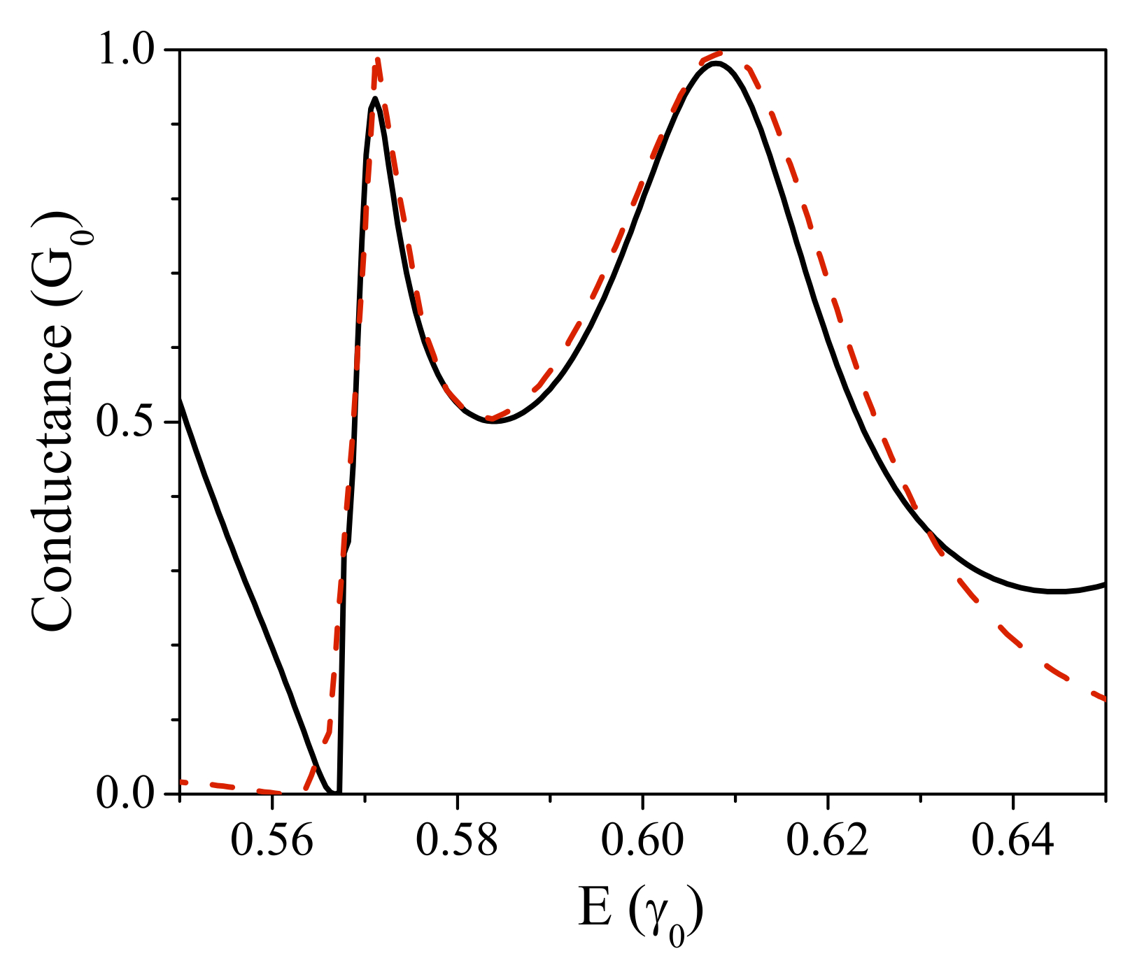
We realize that a possible interference mechanism occurring in our considered system can be explained with the above model, which helps to get an intuitive understanding of the origin of some conductance lines shape. In figure 3 we have plotted a particular conductance resonance and the corresponding fitting given by the model represented by equation (4), where it is observed the good agreement between both curves.
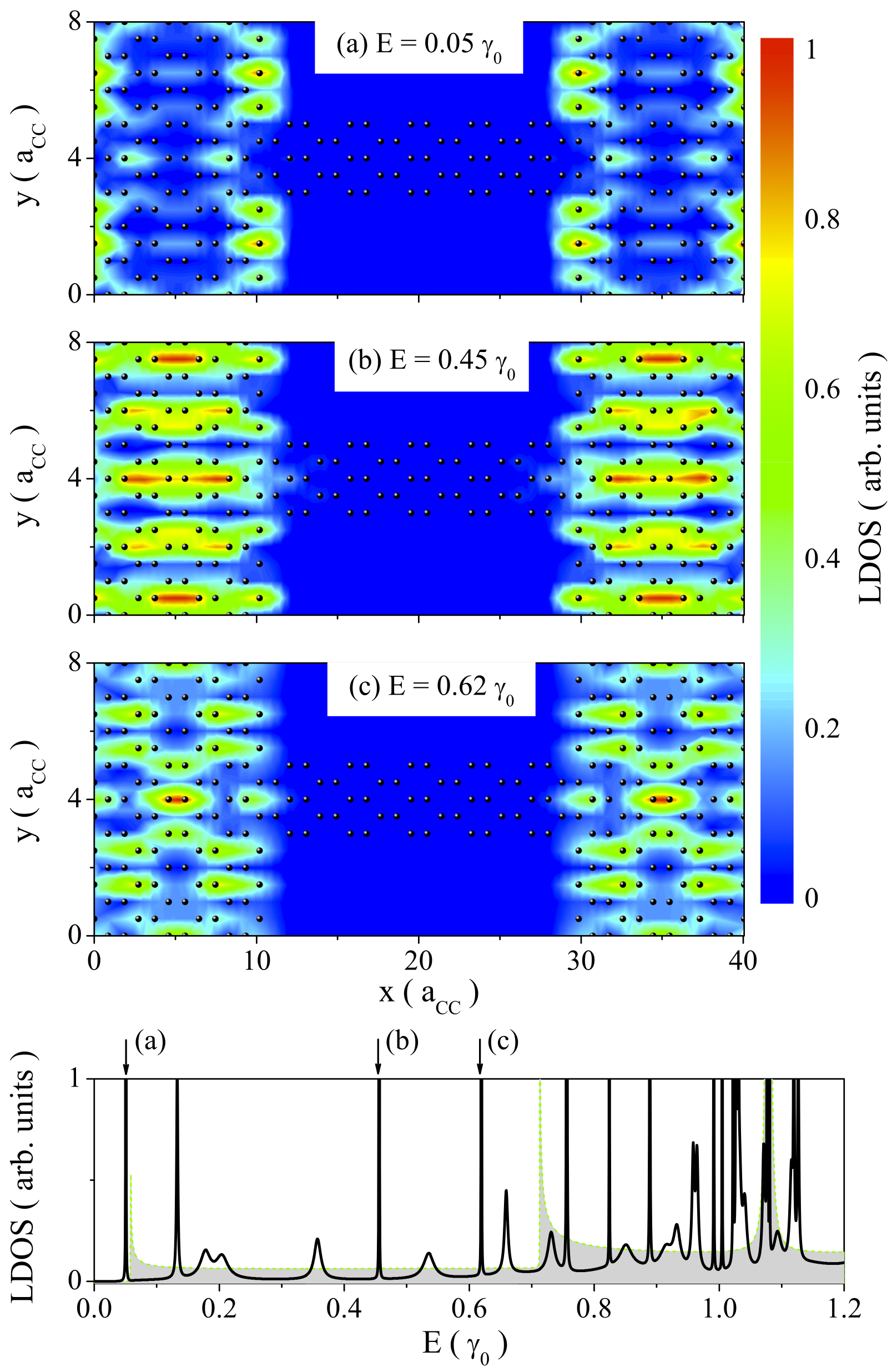
In what follows we focus our analysis on the resonant behavior exhibited by the conductance curves, analyzing the different electronic states in the conductor. We have performed calculations of the spatial distribution of LDOS for certain energies corresponding to different states present in the conductor. In the bottom panel of figure 4 we show results for the LDOS as a function of the Fermi energy, for a GQD structure formed by a double crossbar junction of width and length , separated by a central region of width and length .
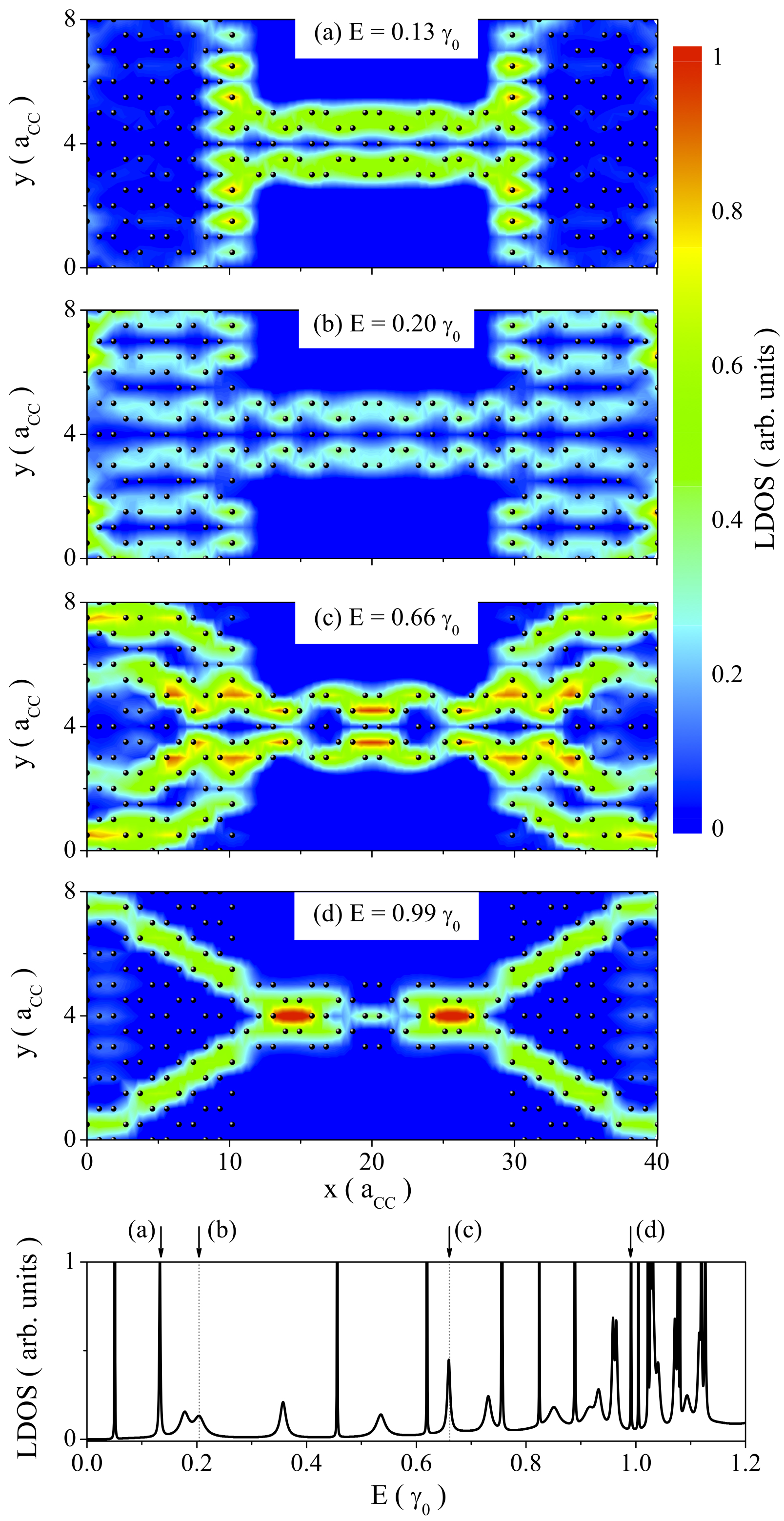
We start our analysis focusing on the some sharp states present in the curve LDOS vs energy of this figure. We have marked the first three sharp states in this LDOS plot with the letters (a), (b) and (c) and we have calculated the spatial distribution of these states, representing by the corresponding contour plots exhibited in the figure. These states are completely localized at the crossbar junctions, and as we establish in a previous workgonzalez2 , their correspond to bound states in the continuum (BICs)wigner ; chinos1 ; pet1 . It is not expected that these kind of states play a role in the electronic transport of these GQD structures, which is shown at the corresponding conductance curves of figure 2.
In what follows we will focus our analysis to those states that contribute to the conductance of the systems. In figure 5 it is shown the spatial distribution of LDOS for a GQD formed by a double crossbar junction of width and length , separated by a central region of width and length . As a reference, at the bottom panel we have included a plot with the LDOS versus Fermi energy of the GQD system, there we have marked with letters (a), (b), (c) and (d) four particular energy states. The corresponding contour plots are displayed at the upper part of the figure.
In these plots, it is possible to observe the resonant behavior of these states, which are completely distributed along the GQD structure, presenting a maximum of the probability density at the center of the system. This condition favors the alignment of the electronic states of the leads with the resonant states in the conductor and consequently, a unitary transmission at those energy values is expected. This behavior is reflected as a series of resonant peaks in the conductance of the system that could be controlled by means of the geometrical parameters of the GQD, as it is shown in figure 2. At higher energies there is an interplay between localized states in the crossbar junctions and resonant states in the central region of the conductor. As it is shown in panel (d) of figure 5, some states are strongly dependent of the geometry of the junctions, therefore for some particular configuration it is possible to observe a non-null transmission at these energies, while for other cases, there are destructive interference mechanisms that suppress completely the transmission at that energy region.
We have studied different configurations of GQDs structures, varying systematically some geometric parameters. We have observed a quite general behavior of such resonant conductors with the presence of sharp and resonant states. Depending of each particular system, it can be observed changes in the number and position in energy of these states, as well as in their spatial distribution. The different intensity of the peaks in the LDOS curves depends on the spatial distribution of the states. There are states completely extended along the conductor (like in panel (b) of figure 5 ) which generate wider and less intense peaks. On the other hand, there are resonant states which are more concentrated in certain regions of the conductor (like as panel (c) and (d) of figure 5) which generate sharper and more intense peaks in the LDOS.
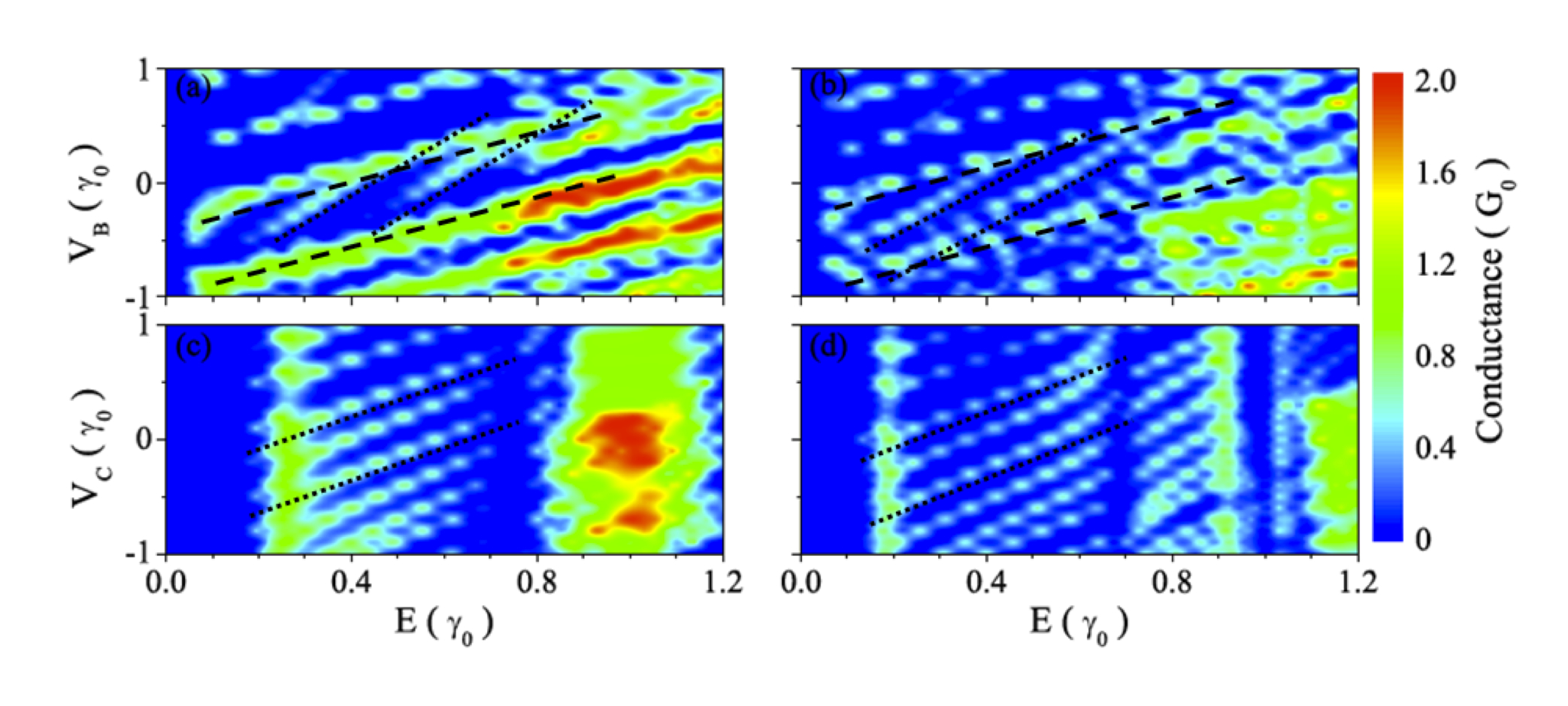
Now we focus our analysis on the effects of an applied gate voltage on the transport properties of GQD structures. Results of the conductance as a function of the Fermi energy, for different values of a gate voltage applied in selected regions of a GQD are shown in figure 6. The systems are composed by leads of width , two crossbar junctions of width , a central part of width and length . Panels (a) and (c) correspond to junctions of length , while panels (b) and (d) correspond to junctions of length . Finally, upper panels correspond to a gate voltage applied at the crossbar junctions regions, whereas the lower panels correspond to a gate voltage applied at the central part of the structure.
In these contour plots of conductance, it is possible to observe the behavior of the resonant states of the system with a gate voltage applied at different regions of the structure. The lower panels of the figure 6 show the case of a gate voltage applied at the central region of the considered GQDs. In these plots the linear dependence of the conductance resonances as a function of the gate voltage is manifested. It can be shown that the electronic states of a pristine armchair graphene ribbon are regularly spaced in the whole energy rangenakada ; wakabayashi , therefore, as the gate voltage is applied, there will be a high probability that the lead states become aligned with the resonant states in the central region of the structure. This behavior in completely general and independent of the width of the crossbar junctions. The linear behavior of the conductance peaks could be useful in nanoelectronics devices, due to the possibility of control the current flow through these systems. This argument will be more clear with the analysis of the differential conductance, which is shown below in this paper.
The case of a gate voltage applied at the crossbar junction regions is shown in the upper panel of figure 6. The conductance behavior in more complicated to analyze, nevertheless it is still possible to observe a linear dependence of the resonant states with the gate voltage. However, two different slopes can be noticed, for states belonging to the crossbar junctions (lower slope) and for states belonging to the central region of the conductor (higher slope). Besides, the panels exhibit an important reduction in the conductance gap, for different values of gate voltage. This effect is mainly produced by an energy shift of the localized states at the junctions, which induces a less destructive interference with the resonant states. It is important to point out that this effect only can be observed because the gate potential is applied simultaneously to both crossbar junctions, otherwise, the conductance gap would be not noticeably affected by the gate potential. Finally, the dark (blue online) regions present in figure 6, occur at energy ranges around the LDOS singularities of the pristine N=5 AGNR. At these energies, it appear the second and the third allowed states appear, which interrupt the linear behavior of the conductance resonances as a function of the gate voltage.
In order to understand the presence of two different slopes in the upper panel of figure 6, we present a simple model which keeps the underlying physics of the considered system and allow us to explain qualitatively our results.
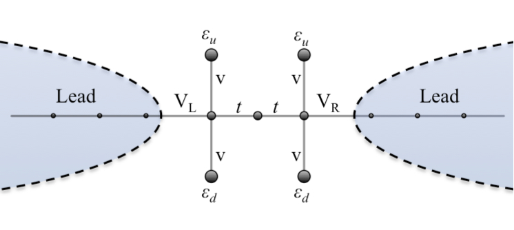
The scheme showed in figure 7 is a simple representation of our conductor. The system is composed by a linear chain of three sites, which are connected to two semi-infinite leads. We have considered four quantum dots connected to the extremes of the chain forming a double crossbar junction, at which we have applied symmetrically a gate voltage . This potential will modify the on-site energy of the dots by a linear shift of energy proportional to the gate voltage amplitude.
By using Dyson equation, it is possible to calculate the Green’s function of the central site of the chain labeled by , which takes the form:
| (5) |
where is the energy of the incident electrons, is the central on-site energy and the self energy is given by the following expression (see Appendix for a detailed deduction):
| (6) |
In this model, the self energy of the Green’s functions of the central region acquires a real part that depends on the gate voltage applied to the crossbar junction region. As a consequence, two different slopes appear in the behavior of the conductance peaks as a function of the gate voltage. One of these slopes corresponds to the direct evolution of the states belonging to the crossbar junctions as a function of the gate voltage (lower slope), and the higher slope corresponds to the indirect states belonging to the central region.
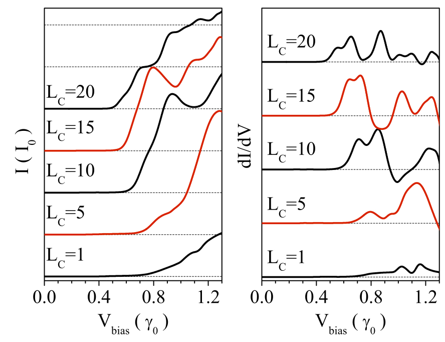
Now we focus our analysis on the I-V characteristics and the differential conductance of these resonant GQDs. Figure 8 shows results of these transport properties for a conductor formed by two crossbar junctions of width , length and a central region of width . In this plots the length of the central structure is varied from up to . In panel (a) it is possible to observe that for a very small separation between both junctions, the I-V characteristics exhibit abrupt slope changes, and oscillations for certain ranges of the bias voltage. This behavior is produced by the increasing number of resonant states as a result of the enlargement of the conductor central region. The applied bias voltage allows the continuum alignment of the resonant states of the system with the electronic states of the leads, leading to variations of the current intensity. On the other hand, every I-V curve shows a wide gap of zero current until certain bias voltage. This threshold value exhibits a linear dependence of the length of the central region of the conductor. As the relative distance between the junctions is increased, there are more resonant states available at lower energies because the electronic confinement in this region is weaker, therefore, the electronic transmission under a bias voltage is possible at lower voltage values.
The abrupt changes of the current as a function of the bias voltage are clearly reflected in the differential conductance of these systems. In panel (b) of figure 8 it is possible to observe the behavior of the curves as a function of the length of the central region of the conductor. As this region is enlarged, the oscillations in the differential conductance become more evident. Each time the bias voltage aligns the resonant states of the conductor with leads states, the current will increase and a positive change in the differential conductance occurs. However, if the bias voltage is not enough to align the states, the current drops and the differential conductance becomes negative in a range of voltage. This can be seen in the cases , and in the figure 8 (b). The bias voltage value at which occurs negative differential conductance (NDC)NDC1 ; NDC2 ; NDC3 depends directly on the relative distance between the crossbar junctions.
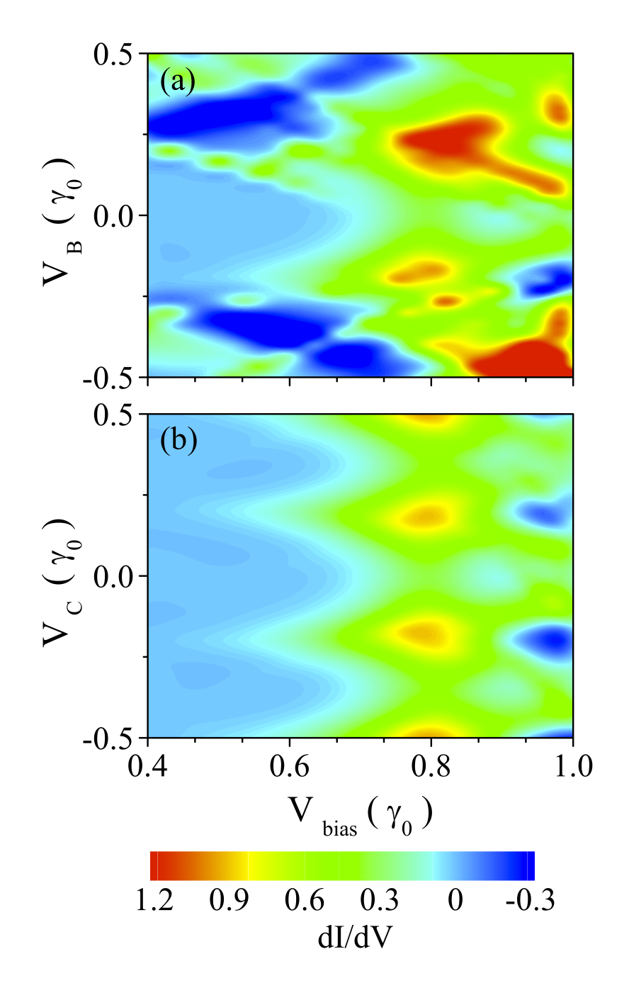
Now we focus our analysis in the effects of a gate voltage on the differential conductance of the systems. In figure 9 we present results of the differential conductance of a GQD composed by two crossbar junctions of length and width separated by a central region of width and length . The gate potential has been applied at selected regions of the structure: (a) crossbar junction regions and (b) at the central region. In panel (b) of this figure it can be observed a periodic modulation of the differential conductance as a function of the gate voltage applied at the central region of the GQD. This behavior is determined and directly related with the linear evolution of the resonant states of the conductor, and consequently, with the peaks of conductance of the system [panel (c) and (d) of figure 6]. For instance, in the configuration considered in this figure, it can be noted abrupt changes of the differential conductance as a function of the gate voltage for bias voltages values around , which indicates an abrupt increasing of the current flowing through the conductor. This behavior is very general for other systems studied, which suggests possible applications in the development of GQDs based electronic devices.
In the case in which the gate voltage is applied simultaneously at the crossbar junction regions, (panel (a) of this figure) it is still possible to note certain regularity in the dependence of differential conductance as a function of the external potentials, although a periodic modulation is not clearly observed. However, in this configuration of applied potentials our results show that the GQD structure exhibits NDC at very low values of bias voltage and gate voltages. This behavior can be understood by observing panels (a) and (b) of figure 6, where the contour plots show areas where the conductance is completely suppressed at low energies, for different values of gate voltage. We have observed this kind of behavior in every configuration considered in this work.
In relation to the practical limitations of our calculations we would like to mention that despite of the size of the structures used in this work are below the limit of the actual experimentally realizable, our calculations can be scaled to structures of bigger sizes. By other hand our model does not include disorder or electron-electron interaction, nevertheless we are convinced that our results will be robust under these kind of effects as it is in mesoscopic systems. For instance it is known that in quantum dots, the resonant tunneling and the Fano effect survive to the effect of the electron-electron interactionKouwenhoven ; kobayashi .
IV Summary
In this work we have analyzed the transport properties of a GQD structure formed by a double crossbar junction made of segments of GNRs of different widths. We have focused our analysis on the dependence of the electronic and transport properties with the geometrical parameters of the system looking for the modulation of these properties through external potentials applied to the structure. Our results depict a resonant behavior of the conductance in the quantum dot structures which can be controlled by changing geometrical parameters such as nanoribbon widths and relative distance between them. We have explained our results in terms of the analysis of the different electronic states of the system. The possibility of modulating the transport response by applying a gate voltage on determined regions of the structure has been explored and it has been found that negative differential conductance can be obtained for low values of the gate and bias applied voltages. Our results suggest that possible applications with GQDs can be developed for new electronic devices.
Acknowledgments
The authors acknowledge the financial support of USM 110971 internal grant, FONDECYT program grants 11090212, 1100560 and 1100672. LR also acknowledges to PUCV-DII grant 123.707/2010.
V APPENDIX: Green’s function of the simple model
In section III, we have introduced a simple model in order to explain the different slopes of figure 6. This model is composed by a linear chain of three sites, of the same energy, at which we have coupled four quantum dots (QDs) of energies ( = u,d), forming a crossbar junction configuration exhibited in figure 7. This simple scheme is very useful to qualitatively explain the electronic behavior of graphene quantum dot that we have studied.
Let us start with the hamiltonian of the system described by figure 7:
| (7) |
where the hamiltonian of the leads is given by:
| (8) |
the conductor hamiltonian is given by;
| (9) |
and finally the leads-conductor hamiltonian is given by:
| (10) |
By using the Dyson equation, it is possible to calculate the Green’ function of site . Following a standard procedure we have obtained:
| (11) | |||||
| (12) | |||||
| (13) |
where and .
Replacing these expression in the previous set of equations, we obtain:
| (14) | |||||
| (15) |
Considering , and replacing the above expressions for and , reads:
| (16) |
where the self-energy is defined by the following expression:
| (17) |
with and .
Using the expressions for the on-sites Green’s functions for the
sites and given by:
and
, and considering a gate voltage
applied to the QDs, which redefine their on-sites energies by
, it is
possible to write an expression for the self-energy of the systems
as:
| (18) |
where we have considered a symmetric system (= ). In this approach, it is possible to write a compact form for the self-energy given in equation (18), which contains a real ( gate voltage dependent) and an imaginary part.
References
- (1) Electronic address: luis.rosalesa@usm.cl
- (2) K. S. Novoselov, A. K. Geim, S. V. Morozov, D. Jiang, Y. Zhang, S. V. Dubonos, I. V. Grigorieva, and A. A. Firsov, Science 306, 666 (2004).
- (3) C. Berger, Z. Song, T. Li, X. Li, A. Y. Ogbazghi, R. Feng, Z. Dai, A. N. Marchenkov, E. H. Conrad, P. N. First, and W. A. de Heer, J. Phys. Chem. B 108, 19912 (2004).
- (4) C. Berger, Z. Song, X. Li, X. Wu, N. Brown, C. Naud, D. Mayou, T. Li, J. Hass, A. N. Marchenkov, E. H. Conrad, P. N. First, W. A. de Heer, Science 312, 1191 (2006).
- (5) X. Li, X. Wang, L. Zhang, S. Lee, H. Dai, Science 319, 1229 (2008).
- (6) L. Ci, Z. Xu, L. Wang, W. Gao, F. Ding, K.F. Kelly, B. I. Yakobson and P. M. Ajayan, Nano Res. 1, 116 (2008).
- (7) D. V. Kosynkin, A. L. Higginbotham, A. Sinitskii, J. R. Lomeda, A. Dimiev, B. K. Price and J. M. Tour, Nature 458, 872 (2009); M. Terrones, Nature 458, 845 (2009).
- (8) B. Oezyilmaz, P. Jarillo-Herrero, D. Efetov, D. Abanin, L. S. Levitov, and P. Kim, Phys. Rev. Lett. 99, 166804 (2007).
- (9) L. A. Ponomarenko, F. Schedin, M. I. Katsnelson, R. Yang, E. W. Hill, K. S. Novoselov and A. Geim, Science 320, 356 (2008) ; J. W. González, H. Santos, M. Pacheco, L. Chico, and L. Brey, Phys. Rev. B 81, 195406 (2010).
- (10) T. G. Pedersen, C. Flindt, J. Pedersen, N. Mortensen, A. Jauho, K. Pedersen, Phys. Rev. Lett. 100, 136804 (2008).
- (11) B. Oezyilmaz, P. Jarillo-Herrero, D. Efetov, and P. Kim, Appl. Phys. Lett. 91, 192107 (2007)
- (12) S. Stankovich, D. A. Dikin, G. H. B. Dommett, K. M. Kohlhaas, E. J. Zimney, E. A. Stach, R. D. Piner, S. T. Nguyen and R. S. Ruoff, Nature 442, 282 (2006).
- (13) F. Schedin, A. Geim, S. Morozov, E. Hill, P. Blake, M. Katsnelson, K. Novoselov, Nature Materials 6, 652 (2007).
- (14) L. Rosales, M. Pacheco, Z. Barticevic, A. Latgé, and P. Orellana, Nanotechnology 19, 065402 (2008); Nanotechnology 20, 095705, 2009.
- (15) C. Stampfer, E. Schurtenberger, F. Molitor, J. Güttinger, T. Ihn and K. Ensslin, Nano Letters 8, 2378 (2008).
- (16) K. Nakada, M. Fujita, G. Dresselhaus and M. S. Dresselhaus, Phys. Rev. B 54, 17954 (1996).
- (17) K. Wakabayashi, Phys. Rev. B 64, 125428 (2001).
- (18) J. W. González, L. Rosales, M. Pacheco, Physica B: Cond. Matt. 404, 2773 (2009).
- (19) B.H. Zhou, W.H. Liao, B.L. Zhou, K. Q. Chen, and G.H. Zhou, Eur. Phys. J. B 76, 421 2010.
- (20) Young-Woo Son, M. L. Cohen, and S. G. Louie, Phys. Rev. Lett. 97, 216803 (2006).
- (21) A. H. Castro Neto, F. Guinea, N. M. R. Peres, K. S. Novoselov, A. K. Geim, Rev. Mod. Phys. 81, 109 (2009).
- (22) M. Nardelli, Phys. Rev. B 60, 7828 (1999).
- (23) S. Datta, Electronic Transport properties of mersoscopic systems(Cambridge University Press, Cambridge, 1995).
- (24) Z.Z. Zhang, Kai Chang and K.S. Chan, Nanotechnology 20, 415203 (2009).
- (25) U. Fano, Physical Review 124, 1866 (1961)
- (26) G. Breit and E. Wigner, Physical Review 49, 519 (1936).
- (27) P.A. Orellana, M.L. Ladrón de Guevara and F. Claro, Phys. Rev. B 70, 233315 (2004).
- (28) J. von Neumman and E. Wigner, Z. Phys. 30, 465 (1929).
- (29) F. OuYang, J. Xiao, R. Guo, H. Zhang and H. Xu, Nanotechnology 20, 055202 (2009).
- (30) A. Matulis and F. M. Peeters, Phys. Rev. B 77, 115423 (2008).
- (31) J. W. González, M. Pacheco, L. Rosales and P. A. Orellana, Europhysics Letters (EPL) 91, 66001 (2010).
- (32) M.Y. Han, B. Ozyilmaz, Y. Zhang, and P. Kim, Phys. Rev. Lett. 98, 206805 (2007).
- (33) V. N. Do and P. Dollfus, J. Appl. Phys. 107,063705 (2010).
- (34) H. Ren, Q. Li, Y. Luo, and J. Yang, Appl. Phys. Lett. 94, 173110 (2009).
- (35) S. M. Cronenwett, T. H. Oosterkamp, and L. P. Kouwenhoven, Science 281, 540 (1998).
- (36) Masahiro Sato, Hisashi Aikawa, Kensuke Kobayashi, Shingo Katsumoto, and Yasuhiro Iye Phys. Rev. Lett. 95, 066801 (2005).