Nanostructures for very broadband or multi-frequency transition from wave beams to a subwavelength light distributions
Abstract
In this paper we suggest and theoretically study a tapered plasmonic nanostructure which connects the incident wave beam with a subwavelength spatial region where the field is locally enhanced in a broad frequency range or for different operation frequencies. This spatial region has a frequency stable location near the contour of the tapered structure. This results from a special waveguide mode which can also exist in the tapered structure. We foresee many possible applications for our structure from prospective near-field scanning optical microscopes to interconnects between conventional optical waveguides and prospective optical nanocircuits.
pacs:
Valid PACS appear hereI Introduction
An actual problem for many branches of the modern optics is the concentration of the light energy initially transported by a conventional wave beam into a subwavelength spatial region. The problem is not new and there is a whole body of literature devoted to so-called subwavelength light concentrators which is difficult to refer in this paper. In most of these works the objective is to achieve very high resolution or very large local field enhancement at a certain frequency. In works on plasmonic nanostructures designed to enhance of thin-film solar cells (see, e.g., Ref. 1) the subwavelength field concentration is achieved together with efficient transmission of the light energy into this region (photovoltaic layer of nanometer thickness). However, as a rule, this subwavelength field concentration is a narrow-band effect. Rarely, it is achievable with the same nanostructure within 2-3 very narrow resonance bands (see, e.g., Ref. 2)
Most sub-wavelength light concentrators such as a solid metal tip with nanoscale curvature of the apex or a nanoantenna operate in the regime when the surrounding space is also illuminated. On the contrary, tapered plasmonic nanostructures, we have unified under the name of metamaterial nanoptips (MMNT),NT1 ; NT2 ; NT3 concentrate the light energy (in our simulations) in a needed sub-wavelength region so that the surrounding space is not illuminated. This way the parasitic excitation of the objects located outside the selected region with the incident wave beam with is avoided. Structures capable of realizing this regime are also not new in the nano-optics. They are actually being used in some schemes of field-enhanced nanosensing, especially of the field-enhanced fluorescence,FEF of the field-enhanced Raman spectroscopy,FES and also in field-enhanced microscopy FEM . Beside these applications, structures which realize such a regime could be used for interconnections between conventional optical information systems and prospective sub-wavelength devices. Sub-wavelength devices which need to be connected with usual optical waveguides are plasmonic nanowaveguides which have developed fast since the past decade,P1 ; P2 optical nanocircuits,Engheta and active all-optical nanodevices (nanoswitches, nanotransistors, nanodiodes and optical memory cells P3 ). In all of these cases the general problem can be formulated as follows: One needs to transmit the optical signal from a conventional waveguide to a needed nano-objects whose locations are known while minimizing the cross-coupling to other nano-objects. This problem formulation recently led to the general idea of a specially shaped (e.g. tapered) waveguide in which the usual wave beam formed by propagating spatial harmonics would concentrate in a sub-wavelength region outside the waveguide, for example, near the end of the waveguide.Stockman We complement this problem formulation by a requirement of a broad frequency range or a multi-frequency operation.
Notice that such a mode concentration was realized in some conventional tips used in scanning near-field optical microscopes (SNOM), namely in those being composed of a conically shaped optical fiber covered with a metal film having a nanometer aperture at the end. However, in such tips the hot spot is located inside the cone which causes almost all the incident wave to reflect from the end of the tip and the energy transmission throughout the tip is very low. Attempts to use the extraordinary transmission effect ET1 ; ET2 for such structures are known. However, only a rather modest improvement of the transmittance was reported in these works and even this modest improvement was achieved by introduction of very complicated nanostructures, for example nanocorrugations in the metal film of the narrowest part of the nanocone.ETNT
More promising results were theoretically demonstrated for our MMNT. In Refs. 3 and 17 tapered waveguides performed as metamaterial prisms (in Ref. 3) it comprised silver nanorods oriented along the prism edge, in Ref. 17 it was formed by silver nanoplates parallel to both the edge and the waveguide axis) efficiently transformed the incident plane wave illuminating the base of the wedge into a light nanojet. The light nanojet is a light beam keeping strongly sub-wavelength width () up to the distance from the nanotip apex. In Ref. 4 a pyramid filled with a metamaterial of plasmonic nanospheres (also illuminated from the base) allowed a very small hot spot (of the order ) at the apex. This light concentration was achieved in these works together with negligible scattering and acceptable reflection losses.
Structures studied in the present paper possess important advantages compared to the pyramidal nanotip reported in Ref. 4. First, they are multi-resonant and the overlapping of resonances can result in a very broad operational frequency band. Secondly, the spatial domain of the enhanced electric field is nearly the same for all operation frequencies. The multi-frequency operation and the frequency stability advantageously distinguish our structure from substantial plasmonic nanoparticles matched to a conventional optical waveguide in Ref. 19. We believe therefore that our MMNT reported will give a significant development to ideas of Ref. 19 and other relevant works published to the present time.
II Suggested structure and its operation
II.1 The main idea
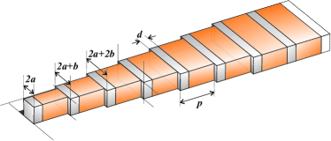
The proposed structure comprises parallel rectangular nanoparticles shaped as nanobars or as nanoplates of noble metal (silver or gold) separated from one another with dielectric spacers (also shaped as nanobars or nanoplates). Both variants are shown in Fig. 1(a) and (b). In the first case the structure width is much larger than its thickness. This MMNT can be located at the dielectric substrate and excited by an integrated (e.g. ribbon) dielectric waveguide having the same substrate. A rather similar multi-resonance structure has been known since 2008 and was called optical xylophone in Ref. 20. However, optical properties of the xylophone structure in which rather wide metal nanobars are separated with narrow spacers are different. The xylophone structure OX would better correspond to our Fig. 1(a) if we replace in this sketch metal and dielectric nanobars. The optical xylophone located at the dielectric interface was excited by an incident plane wave and at a given operation frequency the local field was enhanced near one metal nanoplate resonating at this frequency. Our structure (planar MMNT) is excited by the wave beam impinging the structure from the base of the structure, the field concentration holds in a frequency tangle spatila region, the resonances of different nanoplates overlap and form a very broad frequency range and all this becomes possible due to novel plasmonic waveguide modes that we called the edge modes.
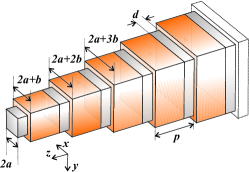
Another MMNT studied below is a pyramid performed of stacked metal nanoplates separated with dielectric spacers Fig. 1(b). This nanostructure can be built at the end of an optical fiber. It seems to be similar to the plasmonic waveguide studied in Ref. 21. However, due to different dimensions the operation of our structure is different from that of the waveguide structure in Ref. 21. The purpose of the study in Ref. 21 was the homogenization of the layered waveguide and the tapered variant of the waveguide was studied in Ref. 21 only in order to demonstrate that the tapering is possible without destruction of the wave guidance. In Ref. 21 plasmon resonances of nanoplates were not exploited. In our study we combine these resonances together with the edge waveguide modes.
In both planar and pyramidal sets of nanoparticles the size of the metal nanoparticles is gradually varied so that the plasmon resonances of the structure cover a sufficient part of the visible range.
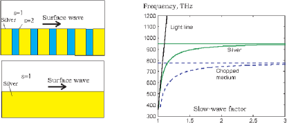
The idea of the surface and edge modes arose from the analysis of surface waves at the interface of the chopped medium with free space. We call as the chopped medium a periodic layered metal-dielectric structure with nanometer period. The sketch of this medium is shown in the left panel of Fig. 2. At the interface of the chopped medium with free space the surface wave excites which has a different dispersion than surface-plasmon polariton (SPP) supported by the interface of the solid metal. The dispersion of SPP for the solid silver sufficiently differs from the light line only within the frequency interval THz. This interval refers to the ultraviolet range. In the visible frequency range the solid silver does not support surface waves. The SPP resonance of the chopped medium occurs in the visible range. In the example of the dispersion diagram presented in Fig. 2 silver layers are of thickness nm and dielectric layers with are of thickness nm, whereas the SPP resonance holds at THz. From to THz (the lower and upper bounds of the visible range) the slow-wave factor is sufficiently larger than unity so that the surface wave could be excited.
Fortunately it is possible to engineer such a wave with the proposed structures because waves propagating along the sides of the wedge- and pyramidal structures can be considered analogous to the surface wave of the chopped medium. A simplified explanation of this effect for a pyramidal structure in Fig. 1(b) is as follows: At a given frequency the incident wave beam excites one of the nanoplates, namely that resonating at this frequency. The local field enhancement happens at the edges of the resonant plate and this local field is a package of evanescent waves. One of these evanescent spatial harmonics excites at the sides of the pyramid a wave propagating from one nanoplate edge to another, i.e., we have a surface-like wave propagating along the sides of the pyramid to its apex. The field of this wave is enhanced compared to the incident wave at the surface of the pyramid and decays in the surrounding space the further it is apart from this surface. If the length of the nanostructure is properly chosen the local field at the apex of the nanostructure will be be enhanced more compared to the sides of the pyramid due to the constructive interference of partial surface waves propagating at four sides of the pyramid. The excitation of nanoplates which are some distant away from the pyramid base is possible if the whole structure is optically rather small and if, for instance, the thickness of silver plates does not exceed nm. So thin silver plates are nearly transparent in the visible.
The operation of the planar structure shown in Fig. 2(b) differs from the pyramidal case only by the dimensionality. The similar edge wave propagating along the sides of the tapered planar waveguide can be excited due to the same physical mechanism. In this case the requirement of the small optical size of the structure can be strongly softened compared to the pyramidal structure. Slender metal nanobars reflect the incident wave beam weakly. Therefore the waveguide mode of the input waveguide can be matched with the mode of the tapered metamaterial waveguide. We called the eigenwave responsible for the operation of both planar and pyramidal structures the edge wave since its electric field is mainly concentrated at the nanobar or nanoplate edges. In order to optimize the tapered structure the edge mode has been analyzed for non-tapered periodic waveguides.
II.2 Dispersion of the edge mode
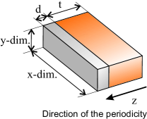
We numerically studied the dispersion properties of a planar periodic plasmonic waveguide whose unit cell is shown in Fig. 3. In this waveguide silver nanobars are sandwiched in between dielectric nanoplates. The dispersion characteristics of such a waveguide were studied using the HFSS simulator whereas the complex permittivity of the silver corresponded to the known experimental data JC and the permittivity of the dielectric was set equal to . The dispersion diagrams for different values of the dimensions (keeping and dimensions fixed) are shown in Figs. 4(a) and (b). The amplitude of the electric field of the different modes at different frequencies are shown in the insets of these Figures. The edge modes shown in Fig. 4(a) propagate on the horizontal side of the waveguide whereas the modes depicted in Fig. 4(b) propagate on the vertical side of the waveguide.
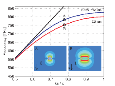
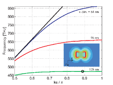
We see that the modes propagating along the horizontal side of the waveguide are less affected by the variation of the dimension of the waveguide whereas the dispersion of the modes propagating along the vertical side of the waveguide is clearly affected by any change in the dimension of the waveguide. For our purposes the mode which is less affected by the tapering of the waveguide in the direction is more favorable. This makes possible the tapering of the waveguide and a large operational frequency band. The apex of the waveguide can be reduced to sub-wavelength dimensions without sacrificing too much in the matching between the wider waveguide sections. The operational band of the wedge is determined by the frequency band over which the dispersion curve of the mode on widest and narrowest waveguide sections overlap. Clearly, we can see that for the vertical edge mode the operational band hardly pushes to the optical regime. For the horizontal edge mode on the other hand the operational band covers the whole optical regime. Further, for both modes the most part of the electric field energy is concentrated near the surface of nanobars, outside their bulk. Therefore the energy absorption in these modes is not so high.
II.3 Plasmonic resonances of nanoparticles
One can roughly estimate the resonance frequencies of an individual nanobar (or nanoplate) replacing it by a slender (or oblate) ellipsoid. For optically small ellipsoids one can use the following condition for the internal electric field :Sihvola
| (1) |
where is the relative permittivity of the surrounding media, is the relative permittivity of the ellipsoid (in our case it is the complex permittivity of silver), and is the depolarization factor along coordinate axes. For the oblate ellipsoids (spheroids) the depolarization factors read:Osborn
| (2) |
| (3) |
where eccentricity .
The resonance frequency becomes then
| (4) |
In these estimations we neglect losses and the permittivity of silver is assumed to obey the Drude dispersion
| (5) |
where is the plasma frequency, is the charger density, is the electron charge, and is the electron mass. Naturally, the estimated resonance frequencies calculated using the above equations are not quite the ones we have for the rectangular nanoparticles, moreover those in presence of dielectric spacers and those coupled with one another through the waveguide mode. Nevertheless, this rough approximation gave us a valid estimation of the resonance frequency range and of the ratio between different resonance frequencies.
III Simulated performance of metamaterial structures
III.1 Planar nanotip

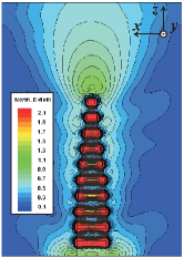
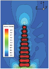
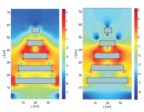
We simulated the performance of the planar MMNT in HFSS. A structure comprising 10 coplanar silver nanobars having thickness nm (dimension in ), length along the waveguide nm (dimension in ), and length across the waveguide (-dim.) reducing from nm to nm, i.e., following the notations in Fig. 1, nm and the length of last 6 nanoplates decreasing with step nm. The structure was excited with a wave port located at the input. The dielectric spacers had length in -dimension (i.e., ) nm and same dimensions in - and -direction as the silver nanobars.
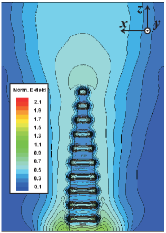
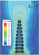
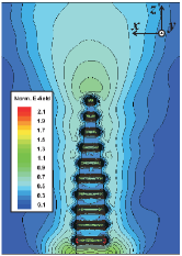
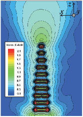
In Figs. 5(a)–(i) we show the distribution of the absolute value of the electric field amplitude normalized to that calculated in absence of the plasmonic structure. The relative field distribution is depicted for the central horizontal plane of the MMNT.
In all these figures the typical field distribution of the edge wave is clearly seen in the narrow part of the MMNT. The field is locally enhanced along the contour of the structure until the distances of nm away from this contour. The amplitude enhancement factor is equal (depending on the frequency). Within the frequency range THz the field decreases fast at larger distances from the contour. Within the frequency region THz the field is enhanced not only along the contour. The constructive interference of two edge waves observes at these frequencies and leads to a hot spot located near the apex. The amplitude enhancement within this hot spot attains (i.e., the intensity enhancement is ). Naturally, even a so large local field enhancement is not comparable with that achievable in self-similar nanolenses.Stock However, the combination of a rather large field enhancement with a relatively large hot spot (its diameter is nm), a stable location of the hot spot in a very broad frequency band makes our structure very attractive, especially if we compare the fabrication costs of our structure to that of a self-similar nanolens. At THz the field enhancement along the contour disappears but the hot spot at the apex keeps. At these frequencies the attenuation of the mode becomes significant.
The main conclusion from Figs. 5 is that the regime which offers the local field enhancement in front of the end of the MMNT refers to the whole frequency region THz which covers percent of the visible range. In this work we do not consider the matching of our nanostructure with a conventional optical waveguide. This problem will be addressed in our next paper.
III.2 Pyramidal nanotip
A systematic study of the pyramidal MMNT is not yet finished. In the present paper we show results which will be hopefully improved in the next future. Geometrical parameters selected below are based only on analytical calculations. Simulations of the nanopyramid were done using the FDTD codes.NT1 ; NT2 ; MMNT Two main differences in the operation of the pyramidal structure from the planar one are as follows: 1) the multi-frequency operation instead of the broadband one since the resonances of the adjacent nanoplates do not overlap, 2) larger local enhancement in the hot spot.
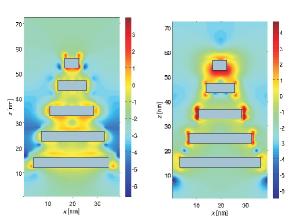
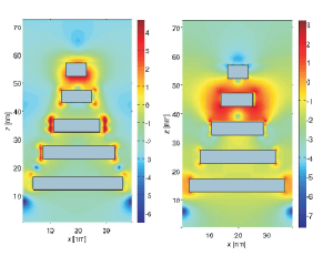
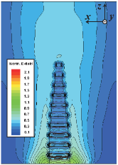
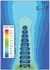
In simulations whose results are depicted in Fig. 6 the whole space around the silver nanoplates was filled with uniform dielectric . Thickness of silver nanoplates in this case was nm as well as the thickness of dielectric spacings between the plates. In Fig. 6 we show logarithmic field distributions , where is the field intensity in presence of nanoplates and is the field intensity in their absence. The distributions are shown in the plane of the pyramid axial cross section. This plane is parallel to the plane in which the incident electric field is polarized. The incident wave beam illuminates the pyramid base and is directed along its axis.
The structure resonates at 9 frequencies ( THz). Each nanoplate has 2 plasmon resonances except the smallest plate whose shape is close to cubic and which has therefore one resonance. For five higher frequencies we obtained the hot spot at the structure apex that we treat as the result of the constructive interferences of edge waves in this spatial region. For four lower resonance frequencies the interference of edge waves near the apex is destructive since the field distribution has a minimum there. However at these four frequencies we obtain nearly the same hot spot between the second or third nanoplates (counted from the apex) because these frequencies correspond to resonances of these two plates in two orthogonal polarizations. So, with this structure we obtain one rather stable hot spot for five discrete resonance frequencies and another stable hot spot at other four frequencies. We also simulated the structure with same nm dielectric spacing between nanoplates but thickness of nanoplates was equal nm. In such a structure similar situation observes with the location of hot spots but the field enhancement in them is significantly larger than that in Fig. 6.
IV Conclusions
In this paper we suggested, theoretically estimated and simulated using the HFSS package and our own FDTD code new tapered nanostructures which is our terminology refer to metamaterial nanotips. These nanotips are formed by rectangular silver nanoparticles, either nanoplates or nanobars alternating with corresponding dielectric spacers which are arranged either in a planar structure or in a pyramidal one. The structures are excited by a wave beam incident from the structure bases. Subwavelength spatial regions are formed around the structure and/or in front of its apex in which the electric field is locally enhanced. In the space surrounding the structure the field is significantly smaller than the incident one. The advantage of our structure compared to known ones is that the subwavelength spatial region of the enhanced field is formed nearly the same at different frequencies. For the planar structure the frequency stability holds over a very broad frequency range. For the pyramidal one this is the stability for several discrete frequencies. We believe that these advantageous properties of our structures and their practical feasibility will not only open new doors in field-enhanced schemes of nanosensing and microscopy, they will be used in prospective nanophotonic applications.
Acknowledgments
This work was partially supported by a joint research grant of Finnish Academy and Russian Foundation for Basic Research in the field of magnetophotonics, plasmonics and nanooptics of heterogeneous metamaterials. Authors are grateful to C. Rockstuhl and S. Mühlig for useful discussion and auxiliary simulations.
References
- (1) K.R. Catchpole, A. Polman, Plasmonic solar cells, Opt. Express, 16, 21793 (2008).
- (2) R.A. Pala, J. White, E. Barnard, J. Liu, M.L. Brongersma, Design of plasmonic thin-film solar cells with broadband absorption enhancements, Adv. Mater., 21, 1 (2009).
- (3) C. Rockstuhl, C.R. Simovski, S.A. Tretyakov, F. Lederer, Metamaterial nanotips, Appl. Phys. Lett., 94, 116951 (2009).
- (4) S. Mühlig, C. Rockstuhl, J. Pniewski, C.R. Simovski, S.A. Tretyakov, F. Lederer, Three-dimensional metamaterial nanotips, Phys. Rev. B, 81, 075317 (2010).
- (5) C. Simovski, J. Pniewski, S. Mühlig, C. Rockstuhl, Multifrequency local field enhancement by a metamaterial nanopyramid, in Proc. of the Days of Diffraction (V. Babich, ed.), St. Petersburg, Steklov Institute, Russian Academy of Sciences, June 5-8, 2010, pp. 78-80.
- (6) O. Stranik, H.M. McEvoy, C. McDonagh, B.D. MacCraith, Plasmonic enhancement of fluorescence for sensor applications, Sensor. Actuator., B107, 148 (2005).
- (7) A. Bek, R. Vogelgesang, K. Kern, Aperture-less scanning near-field optical microscope with 10 nm resolution, Rev. Sci. Instrum., 77, 043703 (2006).
- (8) R. Vogelgesang, J. Dorfmüller, R. Esteban, R. T. Weitz, A. Dmitriev, K. Kern, Plasmonic nanostructures in aperture-less scanning near-field optical microscopy, Phys. Status Solidi (b), 245, 2255 (2008).
- (9) S.I. Bozhevolnyi, Plasmonic Nanoguides and Circuits, Pan Stanford Publishing Pte. Ltd., Singapore, 2009.
- (10) L. Novotny and B. Hecht, Principles of Nano-optics, Cambridge University Press, New York, 2006.
- (11) N. Engheta, Circuits with light at nanoscales: optical nanocircuits inspired by metamaterials, Science, 317 1698 (2007).
- (12) M. Ohtsu, K. Kobayashi, T. Kawazoe, T. Yatsui, M. Naruse, Principles of Nanophotonics, CRC Press, Boca Raton, FL, USA, 2008.
- (13) M. I. Stockman, Nanofocusing of optical energy in tapered plasmonic waveguides, Phys. Rev. Lett., 93, 137404 (2004).
- (14) L. Barnes, A. Dereux, T. W. Ebbesen, Surface plasmon subwavelength optics, Nature, 424, 824 (2003).
- (15) C. Genet and T. W. Ebbesen, Light in tiny holes, Nature, 445, 39 (2007).
- (16) T.J. Antosiewicz, T. Szoplik, Corrugated metal coated tapered tip for scanning near field optical microscope, Opt. Express, 15, 10920 (2007).
- (17) W.M. Saj, T.J. Antosiewicz, J. Pniewski, T. Szoplik, Energy transport in plasmon waveguides on chains of metal nanoplates, Opto-Electron. Rev., 14, 243 (2006).
- (18) X.-W. Chen, V. Sandoghdar, M. Agio, Highly efficient interfacing of guided plasmons and photons in nanowires, Nanoletters, 9, 3756 (2009).
- (19) G. Leveque, O.J.F. Martin, Narrow-band multiresonant plasmon nanostructure for the coherent control of light: an optical analog of the xylophone, Phys. Rev. Lett., 100, 117402 (2008).
- (20) J. Elser, A.A. Govyadinov, I. Avrutsky, I. Salakhutdinov, V.A. Podolskiy, Plasmonic nanolayer composites: coupled plasmon polaritons, effective-medium response, and subdiffraction light manipulation, Journal of Nanomaterials, Vol. 2007, Article ID 79469, doi:10.1155/2007/79469, 2007. 91, pp. 227402, 2003.
- (21) P.B. Johnson, R.W. Christy, Optical constants of the noble metals, Phys. Rev. B, 6, 4370 (1972).
- (22) A. Sihvola, Electromagnetic mixing formulas and applications, IEE Electromagnetic Waves Series 47, IEE, London, UK, 1999.
- (23) J. A. Osborn, Demagnetizing factors of the general ellipsoids, Phys. Rev., 67, 351 (1945).
- (24) K. Li, M.I. Stockman, D. J. Bergman, Self-similar chain of metal nanospheres as an efficient nanolens, Phys. Rev. Lett., 91, 227402 (2003).