A circular dielectric grating for vertical extraction of single quantum dot emission
Abstract
We demonstrate a nanostructure composed of partially etched annular trenches in a suspended GaAs membrane, designed for efficient and moderately broadband ( nm) emission extraction from single InAs quantum dots. Simulations indicate that a dipole embedded in the nanostructure center radiates upwards into free space with a nearly Gaussian far field, allowing a collection efficiency with a high numerical aperture (NA=0.7) optic, and with Purcell radiative rate enhancement. Fabricated devices exhibit a photon collection efficiency with a NA=0.42 objective, a improvement over quantum dots in unpatterned GaAs. A fourfold exciton lifetime reduction indicates moderate Purcell enhancement.
pacs:
78.55.-m, 78.67.Hc, 42.70.Qs, 42.60.DaEfficient extraction of single photons emitted by individual semiconductor epitaxial quantum dots (QDs) is a necessity for many applications in spectroscopy and classical and quantum information processing Shields (2007). As epitaxially grown QDs are embedded in semiconductor material, total internal reflection of the emitted light at the semiconductor-air interface and radiation divergence can typically lead to collection efficiencies even with high numerical aperture (NA) optics. Photonic structures such as micropillar cavities can provide both QD radiative rate Purcell enhancement and a far-field radiation pattern that can be effectively collected Strauf, Stoltz, Rakher, Coldren, Petroff, and Bouwmeester , but require precise spectral tuning of the cavity resonance to the QD emission line. In contrast, vertically-oriented etched nanowires Claudon, Bleuse, Malik, Bazin, Jaffrennou, Gregersen, Sauvan, Lalanne, and Gérard are spectrally broadband structures that have recently been shown to provide large free space collection efficiencies, albeit without Purcell enhancement and with an involved fabrication process. Broadband operation not only relaxes the spectral alignment requirement, which may impose strict constraints in fabrication tolerances, but is also a necessity in spectroscopic applications in which simultaneous detection of various spectrally separate transitions is desired. Here, we present an approach for efficient free space extraction of QD emission using a suspended circular grating. This structure requires a simple nanofabrication procedure, and supports a relatively broad (few nanometer) optical resonance with a directional, nearly Gaussian far-field, which allows efficient free space photon collection. Simulations predict a collection efficiency of % ( %) into a NA=0.42 (0.7) optic. In fabricated devices, we report a single QD photoluminescence (PL) collection efficiency into a NA=0.42 objective, a improvement compared to QDs in unpatterned bulk GaAs. A fourfold reduction in QD lifetime is also observed, indicating moderate radiative rate enhancement.
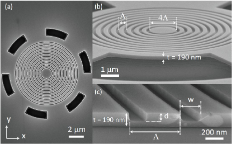
Our nanostructure (Fig. 1) consists of a circular dielectric grating with radial period that surrounds a central circular region of radius , produced on a suspended GaAs slab of thickness nm. The GaAs slab supports single TE and TM polarized modes (electric or magnetic field parallel to the slab, respectively). The grating is composed of ten partially etched circular trenches of width and depth , with . Quantum dots are grown at half the GaAs slab thickness (), and located randomly in the plane. This ’bullseye’ geometry favors extraction of emission from QDs in the central circular region. It is based on (linear) high-contrast second-order Bragg gratings recently introduced Taillaert, Bogaerts, Bienstman, Krauss, Daele, Moerman, Vertuyft, Mesel, and Baets for light extraction from planar waveguides. While similar circular geometries have been employed for enhanced light extraction from light emitting diodes Su and Mirin (2006), and for demonstrating annular Bragg lasers Green, Scheuer, DeRose, and Yariv , here we show an application in QD single photon extraction.
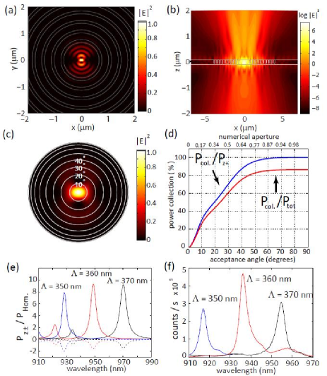
The design process consisted of a series of finite difference time domain simulations that maximized vertical light extraction near the expected QD s-shell emission ( nm), by varying , , and . The structures were excited with a horizontally oriented electric dipole at the bullseye center , representing an optimally placed QD. Total radiated power, steady-state upwards emission, and electromagnetic fields were then recorded at several wavelengths. The grating period was initially chosen to satisfy the second-order Bragg condition, , to allow for efficient vertical light extraction ( is the GaAs slab TE mode effective index). The dipole orientation was assumed to be aligned along the plane, exciting only TE slab waves. Starting values for trench width and depth were nm and , deemed to be easily fabricated. Vertical light scattering at the gratings is partial, so that second-order Bragg reflections towards the center lead to vertically leaky cavity resonances as shown in Figs. 2(a) and (b). The large index contrast at the trenches leads to strong reflections and out-of-slab-plane scattering at the semiconductor-air interfaces, evident in the strong field concentration at the bullseye center in Fig. 2(a) and the fast field decay within the first couple of trenches from the center (Fig. 2(b)). Large differences in propagation constants in the semiconductor and air produce significant resonance spectral shifts with small variations in trench width. Trench depth () has a strong influence on the quality factor () and vertical light extraction, as incomplete spatial overlap between a trench and an incident slab-bound wave leads to both coupling to radiating waves and lower modal reflectivity. Preferential upwards vertical extraction results from the grating asymmetry, and is optimized through the trench depth be_ . We note that in addition to the mode shown in Fig. 1, the cavity supports resonances which can be excited by dipoles offset from the bullseye center. Coupling to these resonances can lead to modified spontaneous emission rates and collection efficiencies be_ .
Figure 2(e) shows simulated, upwards (continuous) and downwards (dotted) vertically extracted power as a function of wavelength for structures with nm, 360 nm, and 370 nm, nm, and . All curves are normalized to the homogeneous medium electric dipole power, . Trench parameters reflect a trade-off in cavity and vertical light extraction, as discussed above. It is apparent that for each , an nm wide resonance exists, with preferential upwards () light extraction. The upwards extracted power is , an indication of Purcell radiation rate enhancement due to the cavity Vučković, Painter, Xu, Yariv, and Scherer . Indeed, for the nm structure, on which we now focus, the enhancement at the maximum extraction wavelength ( nm) is , where is the total radiated power in all directions. This resonance has , and its effective mode volume, calculated from the field distribution, is ( is the GaAs refractive index) be_ . The value for predicted by and is 11.8, and is consistent with the value determined above by the dipole radiation simulations. Note that, given the modal field distribution in Fig. 2(a), the modified dipole emission rate depends strongly on its spatial location, being maximal at the bullseye center.
The steady-state fields at a surface just above the GaAs slab were used to calculate the far-field pattern in Fig. 2(c), which shows that the emission is nearly Gaussian with a small divergence angle. To better quantify this, we calculate the power collected by an optic of varying NA. Figure 2(d) shows the fractions of the upwards emitted () and total () powers collected as a function of the collection optic acceptance angle. For NA= ( acceptance angle), of the upwards emitted power (or of the total emission) can be collected. For NA, or an acceptance angle , collection superior to 80 % of the total emission can be achieved. We note that our suspended grating approach limits radiation into the substrate without the need to oxidize the AlGaAs, bond the grating to a low index layerGreen, Scheuer, DeRose, and Yariv , or utilize a deeply etched geometry Strauf, Stoltz, Rakher, Coldren, Petroff, and Bouwmeester ; Claudon, Bleuse, Malik, Bazin, Jaffrennou, Gregersen, Sauvan, Lalanne, and Gérard .
Gratings were fabricated in a nm GaAs layer containing a single layer of InAs QDs (density gradient from to 0 along the direction) on top of a 1 thick sacrificial layer be_ . Fabrication steps included electron-beam lithography, plasma dry etching, and wet chemical etching. The plasma dry etch was optimized so that the GaAs would be partially etched to a desired depth in the grating region (Fig. 1(b)), and fully etched over the curved rectangles just outside the grating region (Fig. 1(a)), which were used in the wet etching step to undercut and suspend the device.
Testing was done in a liquid He flow cryostat at K. Figure 2(f) shows PL spectra of three devices with a high QD density and 350ñm, 360 nm, and 370 nm and , for pulsed pumping at a 780 nm wavelength (above the GaAs bandgap). The spectra closely resemble the theoretical curves of Fig. 2(e), with three, nm wide peaks spaced by nm. Deviations are likely due to differences in geometry and refractive index between simulated and fabricated structures. These results validated our simulations, and served to calibrate the fabrication process. Figure 3(a) shows PL spectra at various pump powers for a device with nm, now produced in a low QD density region of the sample. Three isolated exciton lines are observed on top of a broad background near 942 nm. The sharp lines red-shift with increasing temperature (Fig. 3(b)) with a dependence that can be fit to a model that predicts a red-shift of the InAs bandgap (Fig. 3(c)) Ortner et al. (2005); Kroner et al. (2009); be_ .
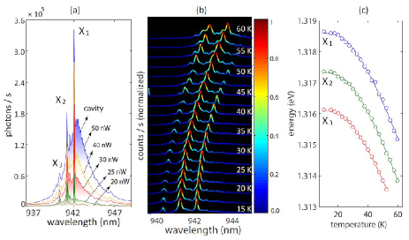
In contrast, the broad background observed in Fig. 3(a) shifts more slowly with temperature, and likely originates from out-coupling of broad QD multiexcitonic emission via the leaky cavity mode Winger, Volz, Tarel, Portolan, Badolato, Hennessy, Hu, Beveratos, Finley, Savona, and Imamoglu . This is reinforced by the observation, in Fig. 3(b), that the sharp QD lines are maximized in the wavelength range , when aligned to the broad cavity peak, and decrease when driven away from it. The slower cavity mode shift with temperature corresponds to a shift in refractive index Badolato, Hennessy, Atature, Dreiser, Hu, Petroff, and Imamoglu .
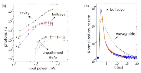
Figure 4(a) shows the detected PL as a function of average pump power for the excitonic lines and and the cavity mode emission from Fig. 3(a). While and saturate at nW, the cavity emission increases past this level. This further supports our assignments of QD transitions and cavity mode in the Fig. 3(a) spectra. Saturated photon rates (collected with a NA=0.42 objective) from and were at least 20 times higher than from typical QDs embedded in unpatterned GaAs, as shown in Fig. 4(a). Assuming 100 % QD quantum efficiency, we estimate a collection efficiency of is achieved with the bullseye pattern be_ . A lifetime measurement of after a pm bandpass filter (Fig. 4(b)) exhibits a multi-exponential decay with a fast lifetime of , limited by the ps timing jitter of the detectors. For comparison, the lifetime of a single QD inside of a suspended GaAs waveguide M. I. Davanço, Rakher, Schuh, Wegsheider, Badolato, and Srinivasan (dotted in Fig. 4(b)), for which no radiative rate modification is expected, was ns. This suggests . Note that since the pump in Fig. 4(a) is pulsed with a 20 ns repetition period, significantly longer than the lifetime, the increase in detected counts relative to unpatterned GaAs is solely due to enhanced photon extraction and collection into the objective.
Improved photon extraction efficiency can potentially be achieved with a higher NA collection optic (50% increase for NA=0.7) and fabrication control be_ , while deterministic QD spatial alignment Hennessy, Badolato, Winger, Gerace, Atature, Guide, Falt, Hu, and Imamoglu ; Thon, Rakher, Kim, Gudat, Irvine, Petroff, and Bouwmeester can enhance both the efficiency and Purcell factor. Although single-photon emission from the bullseye is accompanied by undesirable cavity emission, a few devices exhibited considerably less cavity mode feeding, albeit with lesser extraction efficiencies. Since enhanced extraction efficiency is due to the directional far-field pattern, a trade-off may be achieved between Purcell enhancement and cavity feeding for reduced . It is also likely that quasi-resonant QD pumping will lead to reduced cavity feeding Ates, Ulrich, Reitzenstein, Löffler, Forchel, and Michler . These possibilities are under investigation.
In summary, we developed a nanophotonic circular grating that provides free space collection efficiencies for single InAs QD photons within a wavelength range of nm. Lifetime reduction of at least a factor of four is achieved, which, taken together with the enhanced collection efficiency, indicates Purcell radiative rate enhancement. This structure allows for efficient and broadband spectroscopy of single QDs, and has potential for use as a bright single-photon source.
The authors acknowledge the help of Robert Hoyt. This work has been partly supported by the NIST-CNST/UMD-NanoCenter Cooperative Agreement.
References
- Shields (2007) A. J. Shields, Nature Photonics 1, 215 (2007), eprint 0704.0403.
- (2) S. Strauf, N. G. Stoltz, M. T. Rakher, L. A. Coldren, P. M. Petroff, and D. Bouwmeester, Nature Photonics 1, 704 (2007).
- (3) J. Claudon, J. Bleuse, N. S. Malik, M. Bazin, P. Jaffrennou, N. Gregersen, C. Sauvan, P. Lalanne, and J. Gérard, Nature Photonics 4, 174 (2010).
- (4) D. Taillaert, W. Bogaerts, P. Bienstman, T. F. Krauss, P. V. Daele, I. Moerman, S. Vertuyft, K. D. Mesel, and R. Baets, IEEE J. Quan. Elec. 38, 949 (2002).
- Su and Mirin (2006) M. Y. Su and R. P. Mirin, Applied Physics Letters 89, 033105 (2006).
- (6) W. M. J. Green, J. Scheuer, G. DeRose, and A. Yariv, Appl. Phys. Lett. 85, 3669 (2004).
- (7) See EPAPS supplemental material for details on simulation, nanofabrication, data fitting and quantum dot temperature dependence modeling.
- (8) J. Vučković, O. Painter, Y. Xu, A. Yariv, and A. Scherer, IEEE J. Quan. Elec. 35, 1168 (1999).
- (9) G. Ortner, M. Schwab, M. Bayer, R. Pässler, S. Fafard, Z. Wasilewski, P. Hawrylak, and A. Forchel, Phys. Rev. B 72, 085328 (2005).
- (10) M. Kroner, K. M. Weiss, S. Seidl, R. J. Warburton, A. Badolato, P. M. Petroff, and K. Karrai, physica status solidi (b) 246, 795 (2009), ISSN 1521-3951.
- (11) M. Winger, T. Volz, G. Tarel, S. Portolan, A. Badolato, K. J. Hennessy, E. L. Hu, A. Beveratos, J. Finley, V. Savona, and A. Imamoğlu, Phys. Rev. Lett., 103, 207403 (2009).
- (12) A. Badolato, K. Hennessy, M. Atature, J. Dreiser, E. Hu, P. M. Petroff, and A. Imamoğlu, Science 308, 1158 (2005).
- (13) M. I. Davanço, M. T. Rakher, D. Schuh, W. Wegsheider, A. Badolato, and K. Srinivasan, Appl. Phys. Lett. 99, 121101 (2011).
- (14) K. Hennessy, A. Badolato, M. Winger, D. Gerace, M. Atature, S. Guide, S. Falt, E. Hu, and A. Imamoğlu, Nature (London) 445, 896 (2007).
- (15) S. M. Thon, M. T. Rakher, H. Kim, J. Gudat, W. T. M. Irvine, P. M. Petroff, and D. Bouwmeester, Appl. Phys. Lett. 94, 111115 (2009).
- (16) S. Ates, S. M. Ulrich, S. Reitzenstein, A. Löffler, A. Forchel, and P. Michler, Phys. Rev. Lett. 103, 167402 (2009).
SUPPORTING INFORMATION
.1 Design simulations
The following simulation results illustrate the effects of varying trench depths on emission properties of the circular dielectric grating. Figure 1(a) shows total emitted power as a function of wavelength for various trench depths, and Fig. 1(b) shows the corresponding upwards () and downwards () extracted powers.
Apparent in Fig. 1(a) are a significant central wavelength shift and a strong radiative rate modification. Indeed, as shown in Fig. 1(c), the central wavelength blue shifts more than 40 nm for depths increasing from 95 nm to 190 nm. The resonance full width at half maximum (FWHM), correspondingly, decreases, indicating an increase in field confinement and, consequently, the Purcell Factor (), Fig. 1(e). The increased field confinement for deeper trenches is a consequence of better overlap of the guided field inside the slab and the etched region, which leads to increased guided wave reflectivity and reduces coupling to out-of-plane radiation.
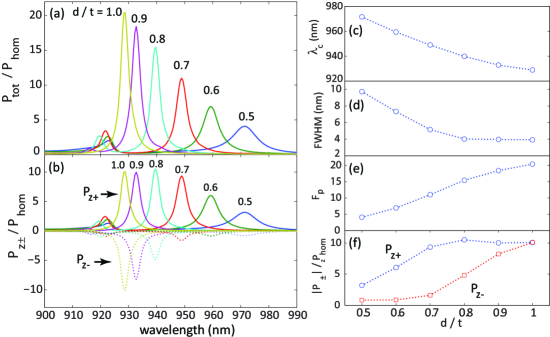
Figures 1(b) and (f) show the effect of grating asymmetry on the ratio between upwards and downwards emitted powers. For a symmetric grating with , emission in both directions is the same. Upwards emission is maximized for , for which . This ratio increases to 5.8 for , however for a reduced . Clearly, a trade-off must be reached between Purcell enhancement and asymmetric emission.
.2 Effective mode volume calculation
The bullseye cavity’s effective mode volume =1.29 quoted in the text was obtained with the expression
| (1) |
where is the modal electric field and the medium permittivity. From and the calculated cavity , we can estimate the maximum Purcell enhacement factor Gérard and Gayral (1999):
| (2) |
where is the refractive index and is the cavity mode wavelength. The value determined through this calculation, , corresponds well with the value that we determine from simulations of the enhanced radiated power for an electric dipole in the bullseye. The above values for assume perfect dipole orientation with respect to the cavity field and optimal dipole location within the field (i.e., in the bullseye center).
.3 Fabrication
Based on simulation parameters, gratings were fabricated on a =190 nm thick GaAs layer containing a single layer of self-assembled InAs quantum dots on top of a 1 thick AlGaAs sacrificial layer. The epiwafer was grown with molecular beam epitaxy, and displayed a quantum dot density gradient from to 0 along the direction. Electron-beam lithography was used to define the patterns, and a single, timed, inductively-coupled plasma reactive ion etch (ICP-RIE) step with an Ar/Cl2 chemistry transferred the gratings into the GaAs. This step was optimized so that the GaAs would be partially etched to a desired depth in the grating region (see Fig.1(b)), and fully etched over the large, curved rectangles just outside the grating region seen in Fig.1(a). These open areas were included to give access to the AlGaAs sacrificial layer, which was etched with Hydrofluoric acid in a final step. Devices with varying quantum dot (QD) densities were produced by fabricating the devices along the QD density gradient of the wafer.
.4 Photoluminescence spectra and collection efficiency
The spectra shown in Fig. 3 were obtained with a grating spectrometer and a Si charge-coupled device (CCD). To obtain the PL intensity from the excitonic lines and in Fig. 3(a) without contributions from the broad cavity background, Lorentzians were fitted to the corresponding peaks. Emitted photon rates plotted in Fig. 4(a) for and and for unpatterned GaAs QD lines correspond to the Lorentzian areas. The integrated cavity photon rates in Fig. 4(b) were obtained by integrating the spectra between 930 nm and 955 nm and subtracting rates from the two excitonic lines.
To estimate the collection efficiency, we convert detected CCD counts to photon counts into our NA=0.42 objective. The two are related by a conversion factor that is equal to the product of our detection efficiency , the transmission through the PL setup , and the transmission through the cryostat windows . includes the in-coupling efficiency into the spectrometer, the spectrometer’s grating efficiency, and the CCD’s quantum efficiency, and is determined by sending a reference laser with known power and wavelength into the spectrometer. In particular, we attenuate a 102 nW laser at 960 nm by 50 dB and acquire a spectrum with a 1 s integration time. Integrating the laser spectrum yielded a count rate of , which, when compared to the photon rate just before the spectrometer (), gives a factor of photons per count. Because the QD emission wavelength ( nm) differs from the calibration wavelength of 960 nm, we multiply this conversion factor by 0.78, which is the ratio of the manufacturer-specified CCD quantum efficiencies at these two wavelengths. We therefore get an overall detection efficiency ( photons per count).
The transmission through the optical path (including the collection objective) was , and was measured by launching a fiber-coupled laser of known power and wavelength through the optical setup. Note that, since the fiber NA=0.13 is less than the objective’s NA, all of the power emitted from the fiber is collected, so the measured transmission includes only transmission losses through the objective and routing optics. , and includes transmission through the radiation shield and outer cryostat windows.
The QD line in Fig. 4(a) yields a saturated CCD count rate of , where the uncertainty is a 95 % fit confidence interval, due to spectrometer resolution and detection noise. Assuming 100 % QD quantum efficiency, the rate of single photons emitted by the saturated QD is equal to the pulsed pump excitation rate, like MHz. The collection efficiency was then calculated as
| (3) |
Substituting all these values yields a collection efficiency .
.5 Quantum dot temperature dependence
The temperature dependence of the sharp features , and in Figs. 3(a) and (b) was fitted with the Bose-Einstein expression
| (4) |
This expression models the evolution of the semiconductor bandgap energy with temperature due to electron-phonon interaction, assuming no phonon dispersion, and has been successfully applied towards excitonic transitions in epitaxially grown quantum dots Ortner et al. (2005); Kroner et al. (2009). In Eq. (4), is the sample temperature, is the excitonic resonance energy, is the phonon energy, and is a dimensionless coupling constant. The fits shown in Fig. 3(c) were obtained with the parameters in Table 1.
The phonon energies in Table 1 are between the bulk GaAs transverse acoustic phonon energies at the X and L points, meV and meV, and the coupling coefficients are compatible with those reported in refs. Ortner et al., 2005 and Kroner et al., 2009. This indicates that the sharp spectral lines correspond to excitonic QD transitions.
| (eV) | |||
|---|---|---|---|
| (meV) | |||
References
- Gérard and Gayral (1999) J.-M. Gérard and B. Gayral, J. Lightwave Tech. 17, 2089 (1999).
- Ortner et al. (2005) G. Ortner, M. Schwab, M. Bayer, R. Pässler, S. Fafard, Z. Wasilewski, P. Hawrylak, and A. Forchel, Phys. Rev. B 72, 085328 (2005).
- Kroner et al. (2009) M. Kroner, K. M. Weiss, S. Seidl, R. J. Warburton, A. Badolato, P. M. Petroff, and K. Karrai, physica status solidi (b) 246, 795 (2009), ISSN 1521-3951.