Optical Rectification and Field Enhancement in a Plasmonic Nanogap
Abstract
Metal nanostructures act as powerful optical antennasMuhlschlegel2005 ; Schuck2005 because collective modes of the electron fluid in the metal are excited when light strikes the surface of the nanostructure. These excitations, known as plasmons, can have evanescent electromagnetic fields that are orders of magnitude larger than the incident electromagnetic field. The largest field enhancements often occur in nanogaps between plasmonically active nanostructuresJiang2003 ; Li2003 , but it is extremely challenging to measure the fields in such gaps directly. These enhanced fields have applications in surface-enhanced spectroscopiesOtto1992 ; Hartstein1980 ; Fort2008 , nonlinear opticsMuhlschlegel2005 ; danckwertsPRL2007 ; bouhelier2003 ; Ghenuche2008 , and nanophotonicsAkimov2007 ; Dionne2009 ; Yu2007 ; Oulton2009 ; Noginov2009 . Here we show that nonlinear tunnelling conduction between gold electrodes separated by a subnanometre gap leads to optical rectification, producing a DC photocurrent when the gap is illuminated. Comparing this photocurrent with low frequency conduction measurements, we determine the optical frequency voltage across the tunnelling region of the nanogap, and also the enhancement of the electric field in the tunnelling region, as a function of gap size. The measured field enhancements exceed 1000, consistent with estimates from surface-enhanced Raman measurementswardNanoLett2007 ; wardNanoLett2008 ; WardJPCM2008 . Our results highlight the need for more realistic theoretical approaches that are able to model the electromagnetic response of metal nanostructures on scales ranging from the free space wavelength, , down to , and for experiments with new materials, different wavelengths, and different incident polarizations.
Published as D. R. Ward, F. Hüser, F. Pauly, J. C. Cuevas, and D. Natelson, Nature Nano. 5, 732-736 (2010), http://dx.doi.org/10.1038/nnano.2010.176
The probability of an electron being able to tunnel across a small gap decays exponentially with distance, so electron tunnelling can be used to measure distances with high precision, as happens in scanning tunnelling microscopy (STM). Moreover, nonlinearity in tunnelling conduction can convert the optical frequency response of the metal into a DC current. This rectification process, originally proposed as a means of inferring the tunnelling timecutlerPRB1987 , allows the optical frequency voltage difference across the tunnelling gap to be determined. Evidence for microwave rectificationtuJCP2006 and optical rectificationnguyenElectronDevices1989 ; bragasAPL1998 has been reported for STM experiments, but thermal and surface photovoltage effectstuJCP2006 complicate interpretation of the optical data.
Suppose that the DC two-terminal current-voltage characteristics of some object are , where is the current and is the DC voltage bias. If the underlying conduction mechanism remains valid at some frequency scale , then in the presence of some small AC voltage bias, , in addition to , one expectstuJCP2006 a total current of
In addition to , in the presence of the AC excitation there is a rectified DC current proportional to the nonlinearity of the conductance and the square of the AC excitation amplitude. As demonstratedtuJCP2006 using STM and microwave irradiation, one may use a low frequency AC voltage and lock-in amplifier to measure using the second harmonic of the AC voltage. Using lock-in techniques to measure the DC current due to microwave irradiation of a known microwave voltage, Tu et al.tuJCP2006 find quantitative agreement between the rectified microwave current and the expectations of Eq. (Optical Rectification and Field Enhancement in a Plasmonic Nanogap).
In the optical case, in the limit that this rectification picture is valid, one would expect the radiation-induced AC response of the metal to lead to a photocurrent, , in addition to the usual DC current, . One may then infer the local, radiation-induced AC voltage, , by comparing and detailed low frequency characterization of the conductance. In a tunnel junction, the differential conductance, , at zero bias can be related to the interelectrode separation through the exponential decay of the conductance with increasing distance, . Here is the internuclear distance between closest atoms, is the size of the metal lattice constant, and is the attenuation factor. The average local electric field at the closest interelectrode separation, , may then be inferred and compared with the incident field known from the incident optical intensity, giving a quantitative measure of the field enhancement due to the metal optical response. The inferred experimentally is that experienced by the optical-frequency tunnelling electrons. Since both and are found from tunnelling, a very local process, this is self-consistent. Voltage drops within the metal far from the tunnelling gap are not relevant. However, there are subtleties to consider, including the role of screening in the metal and the locality of the tunnelling process. We discuss this further in Supplemental Information.
A quantum treatment of radiation interacting with a nanoscale junction involves photon-assisted tunnellingViljas2007 and has been applied to atomic-scale metal contactsguhrPRL2007 ; ittahNL2009 . When a junction is illuminated with radiation of energy , the junction’s plasmonic response results in an AC voltage, at frequency across the junction. Following the Tien-Gordon approachtienPR1963 , the quantum correction to the DC current induced by the radiation in the limit of small AC amplitudes () is given by
| (2) |
If the tunnelling nonlinearity is small on the voltage scale , this expression reduces to Eq. (Optical Rectification and Field Enhancement in a Plasmonic Nanogap) with playing the role of . This occurs when the transmittance of the junction is smooth as a function of energy near the Fermi level of the leads, , throughout .
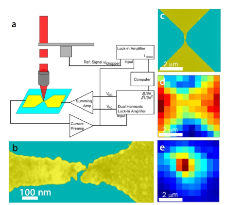
Details of the sample fabrication and the optical and electronic measurements are described in Methods. Nanogaps are formed in the Au constrictions via electromigrationParkAPL1999 . The electromigration process is stopped once the zero bias DC conductance of the gaps is less than . Typical conductances in this experiment are on the order of 0.6 to 0.016 indicating average gaps, , ranging from 0.03 nm to 0.23 nm. Figure 1 shows the measurement system and basic characterization of a representative nanogap. The illumination wavelength is 785 nm, with a peak intensity of 22.6 kW/cm2, and measurements are performed in vacuum at 80 K.
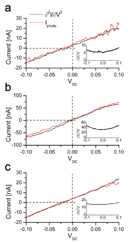
The DC characteristics of the samples after electromigration are weakly nonlinear, with no sharp features, as expected for clean vacuum tunnel junctions. These junctions, ideally devoid of molecules, show no molecular surface-enhanced Raman scattering signalwardNanoLett2007 ; wardNanoLett2008 , as expected. Fig. 2 shows representative vs. curves and simultaneously recorded vs. data for three different samples, acquired with the beam fixed over the nanogap. For each set of curves shown, the amplitude of has been set such that and are the same amplitude. The fact that is directly proportional to consistently over the whole DC bias range, including through the where both change sign, strongly implies that the photocurrent originates from the rectification mechanism. In this case, when , this implies , where is the amplitude of the optically induced voltage between the two electrodes that oscillates at Hz. When the rectification mechanism is responsible for the photocurrent, comparison with low frequency electrical measurements gives a means of quantitatively assessing the plasmon-induced AC voltage across the nanoscale interelectrode gap. As a consistency check, we have mapped the optically rectified current, , at fixed (while monitoring , , and , to ensure junction stability during the mapping procedure). As shown in Fig. 1e, is only produced when the gap itself is illuminated.
Previous tunnelling optical rectification experiments have been hampered by thermal voltages and thermal expansion. We do not expect thermal voltages in our experiment since the device is a comparatively symmetric design, and with a centered laser spot there should be no temperature gradient between the electrodes, even in the presence of minor structural asymmetries. The macroscale unilluminated parts of the electrodes also act as thermal sinks. Differential thermal voltages caused by asymmetry of illumination would show up as systematic trends in as a function of laser position, and Fig. 1e shows no such trends. Thermal expansion should be irrelevant, since the electrodes are intimately mechanically coupled to the substrate, with essentially no unsupported electrode material. To check for thermal effects, we looked for changes in at , since any laser-induced expansion should modulate the interelectrode gap and thus the conductance. No measurable effect was found to better than the level.
Optical rectification is further supported by measurements of vs. incident laser power. In Fig. 3 we see the expected linear dependence. The best fit line has a slope of 0.37 nA/(kW/cm2). Further, as expected, can be selected such that is zero (not always at ), and at that bias measurements show no detectable current.
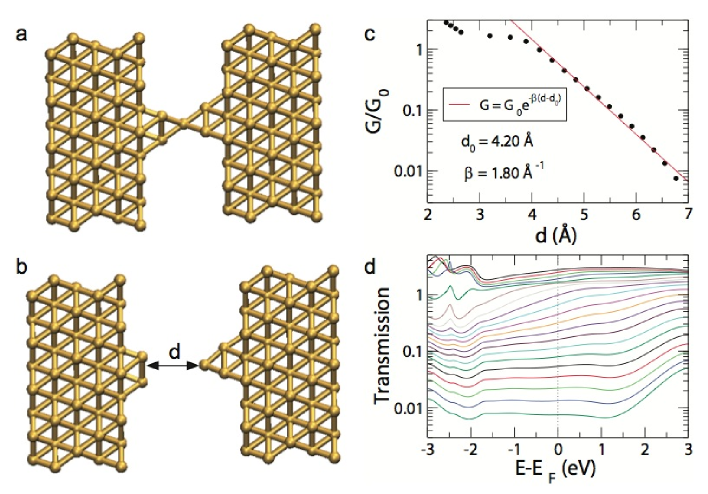
The validity of the rectification picture is not completely obvious for this system a priori. Detailed calculations of the transmission as a function of energy, as shown in Fig. 4, demonstrate that for this particular material and illuminating wavelength, corrections to the classical rectification picture should be relatively small. At higher DC biases ( 100 mV, not shown), we do often observe deviations of the photocurrent from the measured .
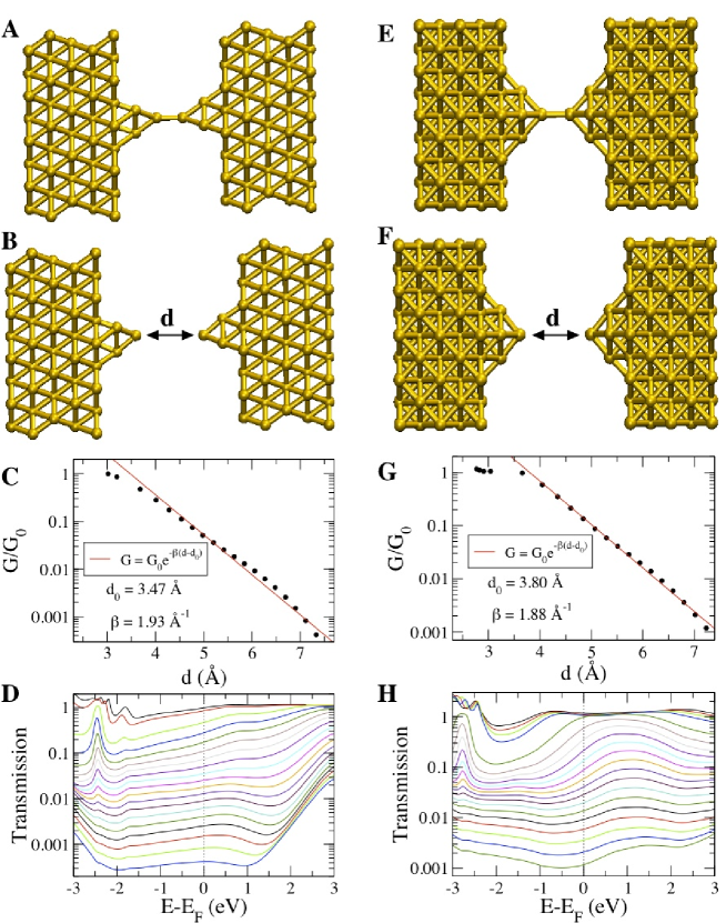
To infer the nanogap size from the conductance measurements, we have performed theoretical simulations of the breaking process of gold atomic contacts. In these simulations, we have used density functional theory to determine the geometry of the junctions as well as to compute the transport properties within the Landauer approach, as detailed in Ref. Pauly2008 . In this approach the low-temperature linear conductance is given by , where is the transmission of the contact evaluated at the Fermi energy, . To simulate the rupture of the gold nanowires, we start out with a single-atom contact (e.g., Fig. 4a). We separate the electrodes stepwise, re-optimize the geometry in every step, and compute the corresponding conductance. As in Fig. 4c, in the relevant range, the linear conductance decays exponentially with an attenuation factor of Å-1. Extensive simulations (Supplementary Information) show that this exponent varies within 10% depending on the geometry of the contact.
Using Å-1 (averaged over different junction structures), the interelectrode gap, , can be found from the measured . With this and the inferred , the enhanced electric field local to the tunnelling gap may be determined. The experimental uncertainty in is approximately 5%, based on the comparisons shown in Fig. 2. The experimental uncertainty in the tunnelling conductance at zero bias is 1%. The dominant uncertainty in the inferred interelectrode separation is systematic, due to variation of with morphology of the metal surfaces. Assuming that is the appropriate scale for computing the local electric field, for the samples in Fig. 2, the optical electric fields (RMS) are V/m, V/m, and V/m, respectively. Based on gaussian beam shape and incident power, the free-space incident RMS field is V/m. Therefore we determine local enhancement factors of the electric field to be 718, 1940, and 1230. These very large enhancements exceed expectations from idealized FDTD calculationswardNanoLett2007 for wider gaps, and are consistent with observations of single-molecule Raman emission in such junctions wardNanoLett2008 ; WardJPCM2008 . At sufficiently high electric field strengths the gap geometry can become unstable. We believe that this is the reason why curves of some devices exhibit instabilities. In the absence of the optical field or at considerably reduced incident laser fluences, the curves are very stable.
Our calculations clarify why the classical rectification formula works in our case. The transmission function (Fig. 4d) of these gold contacts shows only a weak energy dependence around the Fermi energy in the interval . This indicates that the quantum result of Eq. (2) reduces to the classical rectification formula of Eq. (Optical Rectification and Field Enhancement in a Plasmonic Nanogap). This smoothness is because transport in gold contacts is dominated by the atomic orbitals, with a relatively flat density of states. Similar physics should therefore be expected in other -valent metals, such as Ag.
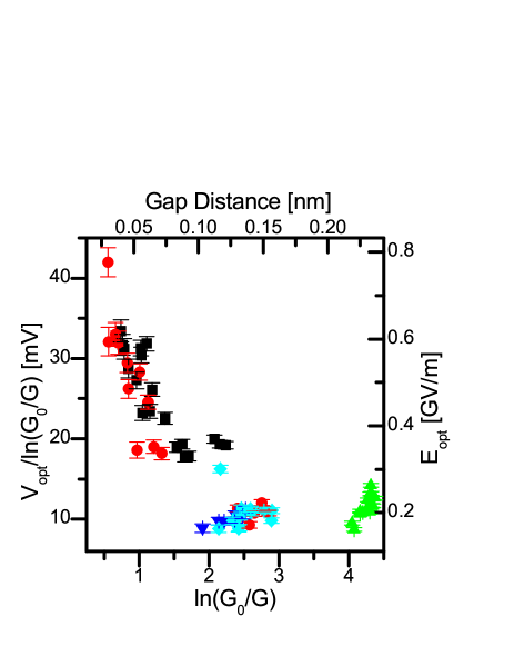
In several devices, conductance decreased over the course of hours of measurements, as the metal electrodes rearranged themselves, allowing us to track variations in (and inferred enhanced electric field) as a function of interelectrode separation (Fig. 5). Despite device-to-device variability, the general trend shows increasing enhancement with decreasing . This trend is slower than and weaker than classical expectationszuloagaNanoLett2009 . Such a comparatively weak increase in enhancement at low is qualitatively consistent with calculations that examine quantum tunnelling corrections to plasmonic enhancements in nanoparticle dimerszuloagaNanoLett2009 ; maoAPL2009 . However, those calculations predict an actual decrease in enhancement when is small enough that interelectrode conductance is strong enough to short out the nanogap plasmons. From our data and previous observationswardNanoLett2008 , this decrease in enhancement does not happen in gold nanojunctions until interelectrode conductance exceeds . Our measurements highlight the need for detailed, realistic theoretical treatments of these nanostructures, incorporating optical interactions, quantum effects, and dynamical screening.
Methods
Samples are fabricated using standard electron-beam lithography techniques to define metal (1 nm Ti/15 nm Au) constrictions 100 nm in width and 600 nm in length between larger contact pads, on highly doped n-type Si substrates covered with 200 nm of thermally grown SiO2. After cleaning in oxygen plasma, devices are wirebonded to a chip carrier, installed in a microscope cryostat, and cooled to 80 K.
After electromigration the sample is illuminated with a 785 nm laser focused to a gaussian spot with FWHM 1.9 m and a peak intensity of 22.6 kW/cm2. The laser is rastered over the sample surface and the Raman response of Si substrate is measured at 520 cm-1. The Au electrodes attenuate the Si Raman emission, allowing precise mapping of the nanogap structure as shown in Fig. 1d. Once the nanogap is located via the Si Raman map, the laser is centered over the gap. The laser polarization is aligned along the original constriction.
The sample is electrically characterized via the apparatus presented in Fig. 1a using two lock-in amplifiers and a current amplifier. The first lock-in amplifier applies an AC excitation () to the sample at = 2.0 kHz and simultaneously measures the first () and second harmonic response () of the nanogap to this excitation. There is no measurable change in either of these responses when the laser illumination is added or removed. The first harmonic response is essentially in phase with the reference. The second harmonic response is phased relative to the reference by 180 degrees as defined by the lock-in, such that the integrated signal gives back the signal. The second lock-in amplifier is referenced to (and in phase with) an optical chopper at = 232 Hz and measures the current generated due to the radiation (). A summing amplifier is used to add a DC voltage to . With this arrangement, , , , and as a function of can be measured simultaneously.
[Supplementary Information] is linked to the online version of the paper at www.nature.com/nature.
[Acknowledgments] D.N. and D.R.W. acknowledge support by Robert A. Welch Foundation grant C-1636 and the Lockheed Martin Advanced Nanotechnology Center of Excellence at Rice (LANCER). F.H. and J.C.C. acknowledge support of the DFG, the Baden-Württemberg Siftung, the EU through the BIMORE network (grant MRTN-CT-2006-035859), and the Spanish MICINN (grant FIS2008-04209). FP acknowledges funding of a Young
Investigator Group.
[Author Contributions] D.R.W. fabricated the devices, performed all measurements, and analyzed the data. D.N. supervised and provided continuous guidance for the experiments and the analysis. F.P., F.H., and J.C.C. carried out the theoretical modeling and DFT calculations. The bulk of the paper was written by D.R.W. and D.N. All authors discussed the results and contributed to manuscript revision.
[Competing Interests] The authors declare that they have no competing financial interests.
[Correspondence] Correspondence and requests for materials should be addressed to D.N. (email: natelson@rice.edu).

References
- (1) Mühlschlegel, P., Eisler, H., Martin, O., Hecht, B. & Pohl, D. Resonant optical antennas. Science 308, 1607-1609 (2005).
- (2) Schuck, P. J., Fromm, D. P., Sundaramurthy, A., Kino, G. S. & Moerner, W. E. Improving the mismatch between light and nanoscale objects with gold bowtie nanoantennas. Phys. Rev. Lett. 94, 017402 (2005).
- (3) Jiang, J., Bosnick, K., Maillard, M. & Brus, L. Single molecule Raman spectroscopy at the junctions of large Ag nanocrystals. J. Phys. Chem. B 107, 9964-9972 (2003).
- (4) Li, K., Stockman, M. I. & Bergman, D. J. Self-Similar Chain of Metal Nanospheres as an Efficient Nanolens. Phys. Rev. Lett. 91, 227402 (2003).
- (5) Otto, A., Mrozek, I., Grabhorn, H., & Akemann, W. Surface enhanced Raman scattering. J. Phys. Condens. Matt. 4, 1143-1212 (1992).
- (6) Hartstein, A., Kirtley, J. R. & Tsang, J. C. Enhancement of the infrared absorption from molecular monolayers with thin metal overlayers. Phys. Rev. Lett. 45, 201-204 (1980).
- (7) Fort, E. & Gresillon, S. Surface enhanced fluorescence. J. Phys. D. - Appl. Phys. 41 013001 (2008).
- (8) Danckwerts, M. & Novotny, L. Optical frequency mixing at coupled gold nanoparticles. Phys. Rev. Lett. 98, 026104 (2007).
- (9) Bouhelier, A., Beversluis, M. R. & Novotny, L. Characterization of nanoplasmonic structures by locally excited photoluminescence. Appl. Phys. Lett. 83, 5041-5043 (2003).
- (10) Ghenuche, P., Cherukulappurath, S., Taminiau, T. H., van Hulst, N. F. & Quidant, R. Spectroscopic mode mapping of resonant plasmon nanoantennas. Phys. Rev. Lett. 101, 116805 (2008).
- (11) Akimov, A. V. et al. Generation of single optical plasmons in metallic nanowires coupled to quantum dots. Nature 450, 402-406 (2007).
- (12) Dionne, J. A., Diest, K., Sweatlock, L. A. & Atwater, H. A. PlasMOStor: A Metal-Oxide-Si field effect plasmonic modulator. Nano Lett. 9, 897-902 (2009).
- (13) Yu, N. et al.. Plasmonic quantum cascade laser antenna. Appl. Phys. Lett. 91, 173113 (2007).
- (14) Oulton, R. F. et al. Plasmon lasers at deep subwavelength scale. Nature 461, 629-632 (2009).
- (15) Noginov, M. A. et al. & Wiesner, U. Demonstration of a spaser-based nanolaser. Nature 460, 1110-1112 (2009).
- (16) Ward, D. R. et al. Electromigrated nanoscale gaps for surface-enhanced Raman spectroscopy. Nano Lett. 7, 1396-1400 (2007).
- (17) Ward, D. R. et al. Simultaneous measurements of electronic conduction and Raman response in molecular junctions. Nano Lett. 8, 919-924 (2008).
- (18) Ward, D. R., Scott, G. D., Keane, Z. K., Halas, N. J. & Natelson, D. Electronic and optical properties of electromigrated molecular junctions. J. Phys.: Condens. Matter 20, 374118 (2008).
- (19) Cutler, P. H. et al. Proposed use of a scanning-tunnelling-microscope tunnel junction for the measurement of a tunnelling time. Phys. Rev. B 35, 7774-7775 (1987).
- (20) Tu, X. W., Lee, J. H. & W. Ho, Atomic-scale rectification at microwave frequency. J. Chem. Phys. 124, 021105 (2006).
- (21) Nguyen, H. Q. et al. Mechanisms of current rectification in an STM tunnel junction and the measurement of an operational tunnelling time. IEEE Trans. Elect. Dev. 36, 2671-2678 (1989).
- (22) Bragas, A. V., Landi, S. M. & Martínez, O. E. Laser field enhancement at the scanning tunnelling microscope junction measured by optical rectification. Appl. Phys. Lett. 72, 2075-2077 (1998).
- (23) Viljas, J. K. & Cuevas, J. C. Role of electronic structure in photoassisted transport through atomic-sized contacts. Phys. Rev. B 75, 075406 (2007).
- (24) Guhr, D. C. et al. Influence of laser light on electronic transport through atomic-size contacts. Phys. Rev. Lett. 99, 086801 (2007).
- (25) Ittah, N., Noy, G., Yutsis, I. & Selzer, Y. Measurement of electronic transport through 1 gold contacts under laser irradiation. Nano Lett. 9, 1615-1620 (2009).
- (26) Tien, P. K. & Gordon, J. P. Multiphoton process observed in the interaction of microwave fields with the tunnelling between superconductor films. Phys. Rev. 129, 647-651 (1963).
- (27) Park, H., Lim, A. K. L., Alivisatos, A. P., Park, J. & McEuen, P. L. Fabrication of metallic electrodes with nanometer separation. Appl. Phys. Lett. 75, 301-303 (1999).
- (28) Pauly, F. et al. Cluster-based density-functional approach to quantum transport through molecular and atomic contacts. New J. Phys. 10, 125019 (2008).
- (29) Zuloaga, J., Prodan, E. & Nordlander, P. Quantum description of the plasmon resonances of a nanoparticle dimer. Nano Letters 9, 887-891 (2009).
- (30) Mao, L., Li, Z., Wu, B. & Xu, H. Effects of quantum tunnelling in metal nanogap on surface-enhanced Raman scattering. Appl. Phys. Lett. 94, 243102 (2009).
Supporting Information:
Optical Rectification and Field Enhancement in a Plasmonic Nanogap
I Tunnelling and field distributions in nanogaps
The experimentally extracted parameter in the rectification measurement is the optical frequency potential difference, , experienced by the tunnelling electrons. To go from this potential difference to an estimate of the enhanced electric field within the tunnelling gap, it is necessary to estimate the distance over which this voltage is dropped. In the main manuscript we use , the interelectrode spacing inferred from the (low frequency) tunnelling conductance. The question arises, is this reasonable given that is oscillating at optical frequencies? There are two relevant issues: the local character of the tunnelling process, and the penetration of electric field (and hence voltage drops) into the metal electrodes.
The rectification process is sensitive to the chemical potential difference experienced by precisely the tunnelling electrons. Because of the local nature of the tunnelling process, the chemical potential difference we infer experimentally is measured between the ”initial” and ”final” positions of the tunnelling electrons. The inferred is the voltage difference that drives the (extremely local) tunnelling process. It is self-consistent to use the gap size extracted from tunnelling conductance as the relevant distance scale, since the local character of the tunnelling electrons is not expected to be frequency dependent (that is, there is no expectation that tunnelling takes place over longer distances at higher frequencies). Additional voltage drops on longer scales within the metal electrodes are perfectly allowed, but not relevant to the inferred since the local tunnelling process is not sensitive to them. The observed consistency between and over the whole bias range would be very difficult to understand if the local nature of the tunnelling process was fundamentally different between low and optical frequencies. This is certainly a subtle issue. The definition of local electrostatic potential and its relationship with chemical potential in nanoscale junctions is not simpleS1, since electronic distributions are driven out of equilibrium on a distance scale comparable to the inelastic scattering length. A full treatment of optical-frequency tunnelling with realistic electronic structure of the contacts (well beyond the scope of the present work) would be needed to resolve this issue unambiguously. The experimentally determined quantities in the main manuscript (tunnelling conductance, ) could be compared with more sophisticated calculations in the future.
Regarding field penetration into the metal, care is also required. The skin depth, which describes the characteristic attenuation length for the electric field of a plane wave normally incident on a metal surface, is related to the complex dielectric function at the incident frequency. For gold at the incident wavelength of 785 nm, the skin depth is approximately 25 nm. However, the skin depth calculation ignores collective electronic response such as plasmons. In fact, in plasmonic nanostructures, while the field due to the incident radiation does penetrate the metal on length scales comparable to the skin depth, the total electric field including that produced by the plasmon response of the electron fluid can be confined much more strongly than this.
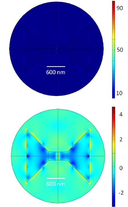
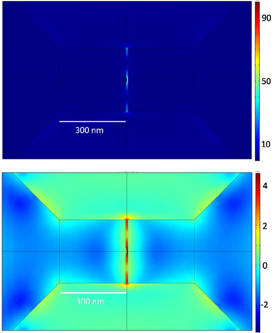
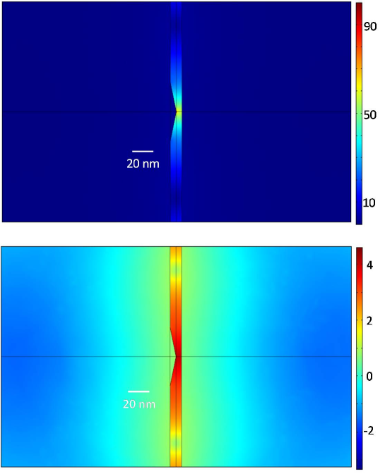
Supplemental Figures S1-S3 demonstrate this explicitly. These figures show the results of a finite element simulation (using the commercial package COMSOL) of a model nanogap structure illuminated at the nanogap plasmon resonance. The figures show top views of the metal structure at three different magnifications indicated by the scale bars. The metal is modeled as Au (using the commonly employed Johnson and Christy dielectric functionS2) 25 nm in thickness (chosen for computational efficiency). The nanogap separation is 10 nm, except in the center of the device, where a protrusion on the left-hand electrode reduces the gap to 5 nm. No dielectric substrate is included, but other models including such a substrate give qualitatively identical results. The incident radiation is assumed to be a plane wave at normal incidence with a free space wavelength of 850 nm and a polarization directed along the line connecting the two electrodes (left-right in the figures). Upper figures show the magnitude of the total electric field (normalized by the incident amplitude) on a linear color scale, while lower figures use a (natural) logarithmic color scale.
It is immediately clear that the vast majority of the potential drop between the two electrodes takes place across the vacuum at the center of the nanogap. Electric field does extend into the metal, but it is smaller than the nanogap field, by a factor of more than 50 in this case, a larger difference than one would expect based on a skin depth analysis that ignores plasmonic effects. For smaller electrode separations, this disparity grows even further, with essentially 100% of the (plasmon-dominated) optically induced potential difference dropping across the vacuum.
The situation is, of course, complicated in the real devices by the true electronic structure of the metal surfaces at the atomic scale, and tunnelling conduction. For very small gaps and distance scales, one must not trust the quantitative accuracy of finite-element or finite-difference time-domain calculations based on idealizations (infinitely sharp dielectric interfaces; bulk-like dielectric functions for the electrons and background charges at interfaces).
However, in plasmon resonant structures such as these, the fact remains that a very large fraction of the potential drop takes place between the electrodes, and the skin depth is not the relevant length scale to describe electric field confinement. The excitation of plasmon collective modes strongly perturbs the charge density extremely local to the surface, leading to field distributions that can differ greatly from those inferred in the absence of such collective effects. For example, LiebschS3,S4 shows that the presence of a surface plasmon excitation in a silver film or nanoparticle dynamically leads to surface charge density within a couple of atomic radii of the surface, with a length scale determined by quantum mechanical electronic structure effects and not by macroscopic electrodynamic effects such as the classical skin depth.
II Theoretical methods
Here we describe in more detail the theoretical methods used for the computation of the structural, electronic, and electrical properties of gold nanocontacts. Moreover, we present an analysis of the geometry dependence of the conductance decay with interelectrode distance.
II.1 Electronic structure and contact geometries
For the determination of the electronic structure and geometry of the gold contacts we employ density functional theory (DFT) as implemented in the RI-DFT module of the quantum chemistry package Turbomole 5.9 S5,S6. In all our calculations we use the open-shell formalism, the exchange-correlation functional BP86 S7,S8, and Turbomole’s standard Gaussian basis set “def-SVP” of split-valence quality with polarization functions S6,S9,S10. Total energies are converged to a precision of better than atomic units, and structure optimization is carried out until the maximum norm of the Cartesian gradients has fallen below values of atomic units.
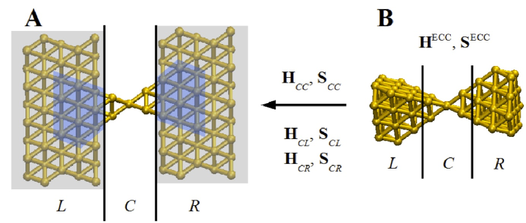
An example of the contact geometries considered in this work is shown in Fig. S4A, which corresponds to the junction of Fig. 4 in the manuscript. In this case, a single-atom contact is modeled by means of the extended central cluster (ECC) with 63 atoms displayed in Fig. S4B. It consists of two pyramids grown along the direction of a fcc lattice, which contain, beside a common tip atom, four layers with 3, 6, 10, and 12 atoms. We formally divide the contact geometry into left (), central (), and right () parts, and relax the atomic positions of the atoms in the region, i.e. those of the tip atom and the neighboring layers with three atoms. In contrast, the atoms in the and regions are kept fixed, and the lattice constant is set to Å, the experimental bulk value for gold.
In order to simulate what happens when the wires are broken and when one enters the tunnelling regime, we stretch the ECC (Fig. S4B) by separating the and regions in steps of 0.4 a.u. ( Å). After every stretching step, the geometries are reoptimized by relaxing the region.
II.2 Conductance calculations
To compute the charge transport properties we apply a method based on standard Green’s function techniques and the Landauer formula expressed in a local nonorthogonal basis, as described in Ref. Pauly2008 . Briefly, the local basis allows us to partition the basis states into , , and ones, according to the division of the contact geometry (Fig. S4). Thus, the Hamiltonian (or single-particle Fock) matrix , and analogously the overlap matrix , can be written in the block form
| (3) |
Within the Landauer approach, the low-temperature conductance is given by , where and is the transmission of the contact evaluated at the Fermi energy. The energy-dependent transmission can be expressed in terms of the Green’s functions asS1:
| (4) |
where the retarded Green’s function is given by
| (5) |
and . The self-energies adopt the form
| (6) |
the scattering rate matrices are given by , and are the electrode Green’s functions with .
In order to describe the transport through the contact shown in Fig. S4A, we first extract and and the matrices and from a DFT calculation of the ECC in Fig. S4B. The blue-shaded atoms in regions and of Fig. S4A are assumed to be those coupled to the region. Thus, and , obtained from the ECC, serve as the couplings to the electrodes in the construction of .
On the other hand, the electrode Green’s functions in Eq. (6) are modeled as surface Green’s functions of ideal semi-infinite crystals. In order to obtain them, we have computed separately the electronic structure of a spherical fcc gold cluster with 429 atoms. By extracting the Hamiltonian and overlap matrix elements connecting the atom in the origin of the cluster with all its neighbors and by using these as “bulk parameters”, we construct a semi-infinite crystal which is infinitely extended perpendicular to the transport direction. The surface Green’s functions are then calculated from this crystal with the help of the decimation technique S11,S12. In this way we describe the whole system consistently within DFT, using the same nonorthogonal basis set and exchange-correlation functional everywhere.
We assume the Fermi energy to be fixed by the gold leads. From the Au429 cluster we obtain eV. Let us point out that the Fermi energy is used only to read off the conductance from the transmission function , but it does not enter into our calculations otherwise.
II.3 Geometry dependence of the conductance decay with interelectrode distance
When an atomic contact is broken, the conductance depends exponentially on the interelectrode distance , i.e. . Here, describes the prefactor of the exponential law and is the attenuation factor. Both constants depend on the surface morphology, in particular on the local atomic environment at the interface region as well as on the crystallographic direction along which the contact is grown. We have studied the influence of these two factors by performing different DFT-based simulations of the breaking process of gold nanowires.
In Fig. S5A-D we show the results obtained for a contact grown along the direction. As compared to the geometry considered in Fig. 4 of the manuscript, the starting geometry is a one-atom-thick contact with a dimer (or two-atom chain) in the narrowest part. We have stretched this contact following the procedure described above (see paragraph “Electronic structure and contact geometries”), and we have computed both the linear conductance and the energy-dependent transmission at the different stages of the elongation process. As it is shown in Fig. S5C, in the range relevant for the experiments, the conductance decays exponentially with an exponent Å-1. This value is approximately 7% larger than the value obtained for the contact of Fig. 4. Furthermore, in Fig. S5D one can see that the transmission is still a smooth function of the energy in a range larger than 1 eV around the Fermi energy.
In Fig. S5E-H we present the corresponding results for a similar contact with a dimer structure, but this time grown along the direction of the fcc lattice. In this case takes a value of 1.88 Å-1, which is 4% larger than those found in Fig. 4. Again, the transmission is a rather featureless function of the energy in the relevant conductance range.
To conclude, we have analyzed different types of gold atomic-sized contacts. Our results indicate that the attenuation factor varies roughly within 10% of the value reported in the manuscript. Additionally, they corroborate that the transmission is a rather smooth function of the energy in an interval of approximately 2 eV around the Fermi energy for the tunnelling regime explored in the experiments.
[S1] Datta, S. Electronic Transport in Mesoscopic Systems. Cambridge Studies in Semiconductor Physics and Microelectronic Engineering (Cambridge University, 1995).
[S2] Johnson, P. B. & Christy, R. W. Optical Constants of the Noble Metals. Phys. Rev. B 6, 4370-4379 (1972).
[S3] Liebsch, A. Surface plasmon dispersion of Ag. Phys. Rev. Lett. 71, 145-148 (1993).
[S4] Liebsch, A. Surface-plasmon dispersion and size dependence of Mie resonance: Silver versus simple metals. Phys. Rev. B 48, 11317-11328 (1993).
[S5] Ahlrichs, R., Bär, M., Häser, M., Horn, H. & Kölmel, C. Electronic structure calculations on workstation computers: The program system turbomole. Chem. Phys. Lett. 162, 165-169 (1989).
[S6] Eichkorn, K., Treutler, O., Öhm, H., Häser, M. & Ahlrichs, R. Auxiliary basis sets to approximate Coulomb potentials. Chem. Phys. Lett. 242, 652-660 (1995).
[S7] Becke, A. D. Density-functional exchange-energy approximation with correct asymptotic behavior. Phys. Rev. A 38, 3098-3100 (1988).
[S8] Perdew, J. P. Density-functional approximation for the correlation energy of the inhomogeneous electron gas. Phys. Rev. B 33, 8822-8824 (1986).
[S9] Schäfer, A., Horn, H. & Ahlrichs, R. Fully optimized contracted Gaussian basis sets for atoms Li to Kr. J. Chem. Phys. 97, 2571-2577 (1992).
[S10] Eichkorn, K., Weigend, F., Treutler, O. & Ahlrichs, R. Auxiliary basis sets for main row atoms and transition metals and their use to approximate Coulomb potentials. Theor. Chem. Acc. 97, 119-124 (1997).
[S11] Pauly, F. et al. Cluster-based density-functional approach to quantum transport through molecular and atomic contacts. New J. Phys. 10, 125019 (2008).
[S12] Guinea, F., Tejedor, C., Flores, F. & Louis, E. Effective two-dimensional Hamiltonian at surfaces. Phys. Rev. B 28, 4397-4402 (1983).