Single-electron shuttle based on a silicon quantum dot
Abstract
We report on single-electron shuttling experiments with a silicon metal–oxide–semiconductor quantum dot at 300 mK. Our system consists of an accumulated electron layer at the Si/SiO2 interface below an aluminum top gate with two additional barrier gates used to deplete the electron gas locally and to define a quantum dot. Directional single-electron shuttling from the source to the drain lead is achieved by applying a dc source–drain bias while driving the barrier gates with an ac voltage of frequency . Current plateaus at integer levels of are observed up to MHz operation frequencies. The observed results are explained by a sequential tunneling model which suggests that the electron gas may be heated substantially by the ac driving voltage.
pacs:
71.55.-i, 73.20.-r, 76.30.-v, 84.40.Az, 85.40.RyWhile the Josephson voltage and the quantum-Hall resistance standards Jeanneret_EPJ_2009 ; Poirier_EPJ_2009 are routinely used in metrology institutes worldwide, the current standard is missing from the so-called quantum metrological triangle which would provide a consistency check for these three quantities. The consistency would remove any remaining doubts about the quantum standards and justify a redefinition of the International System of Units Feltin_EPJ_2009 .
A metallic electron pump with a relative uncertainty of a few parts in in its current has been achieved by utilizing seven tunnel junctions in series, forming six gated islands Keller_APL_1996 . However, the operation frequency was limited to the megahertz range because of adiabaticity requirements for the high number of islands. These low current signals, of the order of 1 pA, are sensitive to thermal fluctuations and hence are not satisfactory for the planned quantum metrological triangle experiments Feltin_EPJ_2009 . Other single-electron pumping experiments have been carried out in different systems such as hybrid normal-metal–superconductor turnstiles Pekola_NatureP_2008 , GaAs/AlGaAs nanowire quantum dots Blumenthal_2007 , InAs nanowire double quantum dots Fuhrer_APL_2007 , metal–oxide–semiconductor field-effect transistors (MOSFETs) in Si nanowires Fujiwara_APL_2008 , and GaAs quantum dots Giblin_NJP_2010 .
In this paper, we employ a silicon quantum dot Angus_NL_2007 shown in Fig. 1(a,b) as a test-bed for the current source. The device was fabricated on a high-resistivity ( 10 k cm at 300 K) silicon substrate. An industry-compatible MOSFET fabrication process is adapted to realize our quantum dot system WHL_APL_2009 . The source and drain were thermally diffused with phosphorus and a high-quality gate oxide was grown thermally yielding a low Si/SiO2 interface trap density of 21010 cm-2eV-1 McCallum_2008 . Two 30 nm wide Al barrier gates with 90 nm separation, defined with electron beam lithography, were subsequently oxidised on a hotplate at 150 ∘C for 5 minutes to form a thin 3–5 nm AlxOy layer Angus_NL_2007 . This layer provides insulation from the overlying top gate which was defined subsequently. An Al plunger gate was defined together with the barrier gates with the purpose of changing the electrochemical potential of the quantum dot.
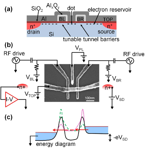
Figure 1(a) illustrates that an electron layer is induced at the Si/SiO2 interface using positive top gate voltages, forming a conduction channel between the source and drain. Two barrier gates (BL and BR) are used to deplete the electron layer and to define a quantum dot between them. The measurement setup is presented in Fig. 1(b) where dc voltages were applied on all gates and the current was measured with a room-temperature transimpedance amplifier connected to the drain. A constant bias voltage was applied to induce a potential difference across the device as shown in Fig. 1(c). To use the device as a single-electron shuttle, rf voltage drives were superimposed on both barrier gate voltages. In our case, we employed two 180∘ out of phase sinusoidal waves, ideally keeping the electrochemical potential of the dot fixed and moving the dot in the lateral direction Kouwenhoven_PRL_1991 . As shown in Fig. 1(c), the dot captures an electron when it is close to the right reservoir with the right barrier gate voltage, , close to its maximum and the left barrier gate voltage, , close to its minimum. To complete a single operation cycle, an electron is ejected when the dot is close to the left reservoir. Thus the dot is analogous to a shuttle taking electrons one by one from the right to the left. An electrostatic simulation using Technology Computer-Aided Design (TCAD) shows that the rf voltages applied to the barrier gates during the shuttling operation induces dot movement in the nanometer scale. In contrast to previously studied electron shuttles Gorelik_1998 , no mechanical degrees of freedom play a role here and the frequency of the electron transport is controlled externally.
Sufficiently low dc voltage levels at the barriers ensure that tunneling can only take place through a tunnel junction when the ac voltage is close to its maximum, and the high ac amplitude renders this process very likely. The charging energy of the dot and the bias voltage determine the number of electrons, , that can tunnel through the device during a single cycle. Ideally, the induced dc current is given by
| (1) |
where is the electron charge and the operation frequency.
Figure 2(a) shows the dc current through the device as a function of the left and right barrier gate voltages with no applied ac driving voltage. Coulomb blockade oscillations near the threshold voltage are observed as diagonal lines. The almost horizontal current maximum near V indicates that there may be a defect below the right barrier. Although we do not employ the defect in the shuttling operation, it may lead to errors in the current and asymmetry in the capacitances between the reservoirs and the dot. Figure 2(b) shows the current through the turnstile during the shuttling operation as a function of the source–drain bias and the plunger gate voltage. We used a peak-to-peak amplitude of = 150 mV as the ac driving voltages on the left and right barriers respectively. Clear current plateaus at multiples of are observed indicating that our qualitative shuttling principle in Fig. 1(c) is in action. The charging energy, , extracted from this plot equals 1.4 meV K, and thus prevents errors due to thermal fluctuations at temperatures K and possibly also from noise Yukinori_JAP_2005 . The total capacitance of the dot is denoted by .
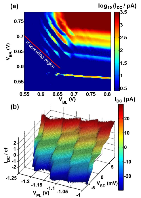
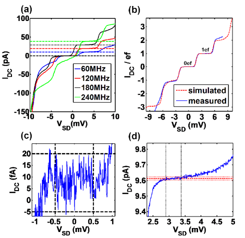
Figure 3(a) shows current plateaus at different frequencies in agreement with Eq. (1) up to 240 MHz. Figure 3(b) shows the shuttle current with parameters tuned to optimize the flatness of the plateaus at currents near and zero. At the plateau near zero current shown in Fig. 3(c), the mean current is 9 fA for ranging from 0.5 mV to 0.5 mV. The origin of this finite current remains unclear.
The plateau for is shown in Fig. 3(d). In contrast to the zero-current plateau, the current near does not achieve its lowest gradient at the center of the plateau but at somewhat lower voltages. Typically for semiconductor single-electron sources, the quantized current is measured at this low-gradient point Blumenthal_2007 ; Giblin_NJP_2010 . This low-gradient point is estimated to be at bias voltages ranging from 2.9 mV to 3.4 mV where we have 29 data points with the mean value 9.6138 pA. This mean value is very close to the ideal current pA. However, the gain of the transimpedance amplifier was calibrated with a 1 G resistor up to 2 nA current with an estimated error of . This calibration yields only 2% accuracy for 10 pA current, and hence we cannot claim the absolute accuracy of the device to be higher than this level. In practice, the calibration is expected to be more accurate since the gain of the amplifier is highly linear and the dominating error in the calibration is likely to arise from the 1 G resistor. The horizontal dotted lines denoting error in Fig. 3(d) illustrate the flatness of the plateau. Even a more pessimistic estimate of the relative error of can be given based on the value of the current not measured at the low-gradient region, but in the middle point of the plateau at mV. The argument for this estimate is that there may exist unknown error processes which tend to decrease the current in their part with increasing bias voltage and hence artificially lower the gradient for a certain bias region. A thorough theoretical analysis and modeling of the different tunneling processes is required to make a definite conclusion whether this is possible.
Figure 3(b) also shows a comparison of the measured current to a simulation result using a sequential tunneling model. The model has been utilized previously for metallic systems Pekola_NatureP_2008 , but in our case the tunneling resistances of the left and right barrier were taken to depend exponentially on the respective gate voltage. This dependence was chosen to agree with the measurement in Fig. 2(a). The capacitance values were primarily extracted from dc measurements but a slight fine tuning was carried out to fit well with the experimental data due to issues such as the difference in the attenuation in the rf lines. In addition, a shift of 0.1 mV was applied to the source–drain bias justified by the non-vanishing input voltage of the transimpedance amplifier. It turned out that the sequential tunneling model did not agree with the measurements if the temperature of the cryostat thermometer, 300 mK, was used. Instead, an electron temperature of 1.5 K gave the good fit shown in Fig. 3(b). In the case of no rf driving, a good agreement with the measurements of the current–voltage characteristics near Coulomb blockade was obtained if the temperature was set to 300 mK in the simulation (data not shown). This suggests that the source and drain electron reservoirs may heat up due to the rf drive of the barrier gates. Thus the high charging energy of the dot is essential to prevent errors from the thermal fluctuations. In future, we aim to improve our model to be able to compare the shuttle current up to high accuracies at the plateaus shown in Fig. 3(c,d).
Our studies show also that the asymmetry in the capacitance from the dot to the left and right reservoirs, or the asymmetry in the amplitudes of the sinusoidal gate drives, can cause the electrochemical potential of the dot to oscillate during the control cycle. This in turn has the effect that the current plateaus at negative and positive bias are of different quality. If the asymmetry is large enough, a plateau at can appear at zero or even negative bias. To compensate for this uncontrolled asymmetry, we suggest the use of a third rf driving voltage on the plunger gate and an improved coupling to the plunger gate WHL_APL_2009 .
In summary, the single-electron shuttle is a promising current source with demonstrated current plateaus at a few tens of pA. Although these results are still far from the requirements of a metrological current standard, sample and pulse sequence optimization has the potential to improve the accuracy and yield to the desired level.
The authors thank D. Barber, R. P. Starrett, and J. Szymanska for technical support, and J. P. Pekola for discussions and cryostat time. We acknowledge Academy of Finland, Emil Aaltonen Foundation, and Technology Industries of Finland Centennial Foundation for financial support. This research was also supported in part by the Australian National Fabrication Facility, the Australian Research Council Centre of Excellence for Quantum Computation and Communication Technology (project number CE110001029), and by the U. S. National Security Agency and U. S. Army Research Office (under Contract No. W911NF-08-1-0527).
References
- (1) B. Jeanneret and S. P. Benz, Eur. Phys. J. ST 172, 181 (2009).
- (2) W. Poirier and F. Schopfer, Eur. Phys. J. ST 172, 207 (2009).
- (3) N. Feltin and F. Piquemal, Eur. Phys. J. ST 172, 267 (2009).
- (4) M. W. Keller, J. M. Martinis, N. M. Zimmerman, and A. H. Steinbach, Appl. Phys. Lett. 69, 1804 (1996).
- (5) J. P. Pekola, J. J. Vartiainen, M. Möttönen, O. Saira, M. Meschke, and D. V. Averin, Nature Phys. 4, 120 (2008).
- (6) M. D. Blumenthal, B. Kaestner, L. Li, S. Giblin, T. J. B. M. Janssen, M. Pepper, D. Anderson, G. Jones, and D. A. Ritchie, Nature Phys. 3, 343 (2007).
- (7) A. Fuhrer, C. Fasth, and L. Samuelson, Appl. Phys. Lett. 91, 052109 (2007).
- (8) A. Fujiwara, K. Nishiguchi, and Y. Ono, Appl. Phys. Lett. 92, 042102 (2008).
- (9) S. P. Giblin, S. J. Wright, J. D. Fletcher, M. Kataoka, M. Pepper, T. J. B. M. Janssen, D. A. Ritchie, C. A. Nicoll, D. Anderson, and G. A. C. Jones, New J. of Phys. 12, 073013 (2010).
- (10) S. J. Angus, A. J. Ferguson, A. S. Dzurak, and R. G. Clark, Nano Lett. 7, 2051 (2007).
- (11) W. H. Lim, H. Huebl, L. H. Willems van Beveren, S. Rubanov, P. G. Spizzirri, S. J. Angus, R.G. Clark, and A.S. Dzurak, Appl. Phys. Lett. 94, 173502 (2009).
- (12) J. McCallum, M. Dunn, and E. Gauja, Mater. Res. Soc. Symp. Proc. 1074, I12-15 (2008).
- (13) L. P. Kouwenhoven, A. T. Johnson, N. C. van der Vaart, and C. J. P. M. Harmans, Phys. Rev. Lett. 67, 12 (1991).
- (14) L. Y. Gorelik, A. Isacsson, M. V. Voinova, B. Kasemo, R. I. Shekhter, and M. Jonson, Phys. Rev. Lett. 80, 4526 (1998).
- (15) Y. Ono, A. Fujiwara, K. Nishiguchi, H. Inokawa, and Y. Takahashi, J. Appl. Phys. 97, 031101 (2005).