0.765 in0.765 in0.4 in0.4 in
Classical Analogue of Electromagnetically Induced Transparency with a Metal/Superconductor Hybrid Metamaterial
Abstract
Metamaterials are engineered materials composed of small electrical circuits producing novel interactions with electromagnetic waves. Recently, a new class of metamaterials has been created to mimic the behaviour of media displaying electromagnetically induced transparency (EIT). Here we introduce a planar EIT metamaterial that creates a very large loss contrast between the dark and radiative resonators by employing a superconducting Nb film in the dark element and a normal metal Au film in the radiative element. Below the critical temperature of Nb, the resistance contrast established opens up a transparency window along with a large enhancement in group delay, enabling a significant slowdown of electromagnetic waves. We further show that superconductivity allows for precise control of EIT response through changes in the superfluid density. Such tunable metamaterials may be useful for telecommunication purposes because of their large phase shifts and delay-bandwidth products.
pacs:
42.70.-a,42.50.Gy,41.20.JbElectromagnetically induced transparency (EIT) is a quantum mechanical effect observed in three-level atomic systems in which a beam of light can find its way through the medium with almost no absorption Matsko et al. (2001); Fleischhauer et al. (2005). The typical configuration involves two atomic states which can be independently excited to the same final state, but have a forbidden transition between them. A probe beam tuned near one allowed transition will show a Lorentzian absorption profile. In the presence of a coherent pump beam exciting the other allowed transition, there can be interference that produces a narrow transparency window for the probe beam, with simultaneously strong dispersion resulting in a significant enhancement of the group delay and the possibility of slowdown/storage of light Hau et al. (1999); Fleischhauer and Lukin (2000); Liu et al. (2001); Bajcsy et al. (2003).
The characteristics of EIT can be reproduced by a classical resonator model based on two oscillating masses coupled by a spring Garrido Alzar et al. (2002). One mass with dissipation factor is acted upon by an external force, whereas the other mass with dissipation of is not driven directly. If , a greatly minimized absorption and steep dispersion are visible at a particular driving frequency, due to a superposition of normal modes with almost zero displacement of the lossy oscillator.
Several groups have recently demonstrated classical analogues of EIT, mostly with electromagnetic metamaterials made of resonant artificial elements Fedotov et al. (2007); Papasimakis et al. (2008); Tassin et al. (2009a); Papasimakis et al. (2009). One approach is to create an array of rings with asymmetric splits enabling the excitation of trapped-current modes Fedotov et al. (2007). Another study has utilized a continuous fish-scale pattern to excite those normally inaccessible modes Papasimakis et al. (2008). Highly symmetrical geometries have also been proposed, e.g., an array of double ring resonators for which the response does not depend on the polarization Papasimakis et al. (2009) and two mirrored split-ring resonators (SRRs) with a cut wire at the center achieving enhanced transmission without breaking the symmetry Zhang et al. (2010). Apart from metamaterials showing EIT at microwave frequencies, plasmonic structures have been designed Zhang et al. (2008) to create similar characteristics at optical frequencies Liu et al. (2010).
Earlier efforts to demonstrate classical EIT using normal-metal electromagnetic oscillators have suffered from insufficient loss contrast between the dark and radiative resonators. Here, we present a design with a resistance contrast that is several orders of magnitude larger than previously reported. The proposed artificial molecule (metamolecule) of our metal/superconductor hybrid metamaterial consists of a double planar SRR made of a superconducting Nb film symmetrically located around a normal-metal (Au) strip (see the Supporting Material for the details of the design and fabrication). Use of Nb limits operation to the sub-THz band; using a high- superconductor instead of Nb might allow scaling of our structure to THz frequencies. The Au strip is oriented along the electric field of the fundamental waveguide mode and is designed to have an electric dipole resonance around = 10.6 GHz; it is thus the radiative element in the metamolecule. Each of the two SRRs have in general an electric dipole resonance (currents in both arms flowing in the same direction) and a magnetic dipole resonance (currents in both arms flowing in opposite directions, i.e., current circling around the SRR) NotePeaks . The position of the gaps in the SRRs has been chosen such that the electric field of the fundamental waveguide mode cannot excite their magnetic dipole resonance. In a free space experiment, the gaps would have been in the middle of the SRRs, but here they are shifted towards the center in order to account for the mode profile of the incident wave. In this way, the magnetic dipole mode of the SRRs can be used as the dark mode in our metamaterial.
Furthermore, the geometry has been optimized to increase the loss contrast between the radiative (strip) and dark (SRRs) resonators. Firstly, the width of the strip is small to increase its resistance. Secondly, the mirror symmetry of the double SRR avoids magnetic dipole radiation of the dark element Zhang et al. (2010). In order to enhance the loss contrast, we have made the SRRs from a Nb thin film. Below the of Nb, the microwave surface resistance of the dark element will be very small (about at and ) Pambianchi et al. (1994). In contrast, the strip is made of a normal metal that retains significant surface resistance at low temperatures.
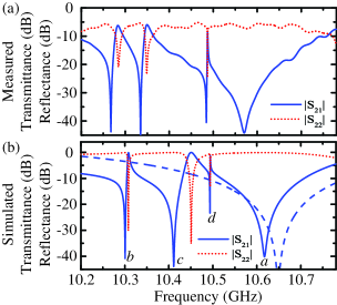
We have performed the microwave transmittance and reflectance measurements on this metamaterial by placing the metamolecule in a Nb X-band waveguide. We have cooled the system down below the of Nb, and measured the scattering parameters. In the transmittance spectrum in Fig. 1(a), we observe a broadband dip with three narrow resonance-shaped features with increased transmittance. This is quite different from earlier works Fedotov et al. (2007); Papasimakis et al. (2008); Tassin et al. (2009a); Papasimakis et al. (2009); Zhang et al. (2010) where only one narrow transmission peak is observed. The reflectance data give sharp dips in each transparency window where the transmittance is enhanced. The underlying Lorentzian stopband [dashed curve in Fig. 1(b)] is due to the electric dipole interaction between the wire and the incident field. It can also be shown from a simple coupled-resonator model Garrido Alzar et al. (2002); Tassin et al. (2009a) that the resonance-shaped features emerge when a dark resonator is coupled very weakly to the radiative resonator and when the dark resonator is of sufficiently high quality. The question that remains to be addressed is why we find three of these features in our experiment.

Our simulations (see the Supporting Material for details) can reproduce the experimental transmittance spectrum to a high degree of similarity [Fig. 1(b)]. We find that there is only one EIT-like transmission window if the sample is positioned with perfect symmetry in the waveguide, and that the two additional EIT features appear as soon as this symmetry is slightly broken, i.e., by slightly tilting or shifting the metamolecule, or even by using a mesh that lacks the required symmetry. Such deviations from the ideal position will undoubtedly be present in the experiment. This suggests that there are two extra dark modes that are uncoupled to the wire if symmetrically located, but having a nonvanishing coupling as soon as the symmetry is broken.
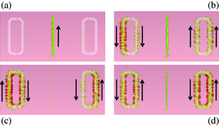
Further evidence for this hypothesis can be gained from the current distributions obtained from the simulations shown in Figs. 2(a)-(d). In Fig. 2(a), displaying the current distribution at = [the feature labeled a in Fig. 1(b)], there is a large current density in the wire only; this is the electric dipole resonance of the wire. At the EIT feature at = [b in Fig. 1(b)], we see large currents in the SRRs and only a little current in the wire commensurate with a dark mode excitation [Fig. 2(b)]. The current distribution reveals that this dark mode is one of the hybridizations of the electric dipole resonances of the SRRs. We see that the currents in the two different SRRs flow in opposite directions. Therefore, if the metamolecule is perfectly at the center of the waveguide, there will be no coupling between the wire and this dark mode and, hence, no EIT effect. However, if the symmetry is slightly broken, the currents in the two SRRs are no longer exactly opposite and a small coupling may be achieved. The EIT feature at = [c in Fig. 1(b)] has the main currents circling around the SRRs—one in a clockwise direction, the other in a counterclockwise direction [Fig. 2(c)]; this is the symmetric hybridization of the magnetic dipole resonances of the SRRs that was observed in earlier work Zhang et al. (2010). At the frequencies inside the EIT feature at = [d in Fig. 1(b)], the current density is again circling the SRRs, but now in the same direction for both SRRs [Fig. 2(d)]; this is the antisymmetric hybridization of the magnetic dipole resonances of the SRRs. It may again be inferred from symmetry considerations that this hybridization has vanishing coupling to the electric dipole mode of the strip only if the molecule is positioned exactly in the middle of the waveguide. These considerations explain the origin of the three EIT features; the resonance shape of the features is explained by constructive (destructive) interference of the current induced in the wire by the SRRs and the current directly excited by the external wave for the peak (dip) in transmittance.

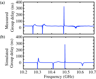
We now proceed with our measurements of the group delay [Fig. 3(a)] Note , which are reproduced well by the simulations [Fig. 3(b)]. We observe significantly enhanced group delay inside the three EIT transmission windows, in particular for the highest-frequency EIT feature for which we find a group delay above . Indeed, the group delay enhancement is related to the linewidth of the EIT feature, which is in turn determined by the coupling strength Tassin et al. (2009). Since the coupling of the highest-frequency dark mode is introduced by a slight misalignment, it can be made arbitrarily small, unlike the middle EIT feature for which the maximal group delay is limited by the overall size of the metamolecule. With the use of a superconductor, we can now achieve large group delays from a subwavelength thin metamolecule, which may find application as compact delay lines with phase shifts on the order . The delay-bandwidth product (DBP) of our structure is 0.3, which approaches the DBPs in resonant cavities (DBP ), but is still smaller than media containing atomic vapors (DBP ) and some photonic crystal waveguides that can achieve a DBP over 100, but we should keep in mind that the latter systems are much longer than a single wavelength Baba et al. (2009).

The reader should also note the transmittance contrast of about between the peaks of the EIT windows and the transmittance dip associated with the wire response. This has to be compared with less than 10 dB for normal-metal EIT metamaterials with similar geometry Zhang et al. (2010), i.e., a difference of three orders of magnitude. The significantly improved transmittance contrast is the direct consequence of the reduced loss in the dark element by employing a superconductor. The presence of the superconductor is critical in this experiment because the weakly-coupled EIT resonances with large group delay are very sensitive to loss and would be destroyed if a superconductor were not used.
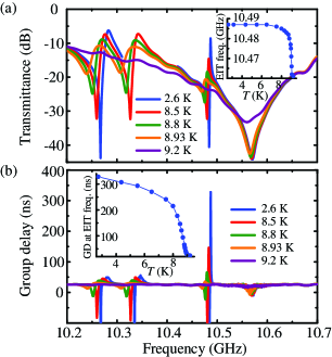
We investigate now the temperature dependence of the metamaterial response. We have plotted the measured transmittance [Fig. 4(a)] and group delay [Fig. 4(b)] for a set of temperatures. The enhancement of the transmittance and the group delay [inset of Fig. 4(b)] both decrease with increasing temperature. This is due to the increase in ohmic loss of the superconductor, originating from a larger fraction of electrons in the normal state, which at high temperatures finally leads to an insufficient loss contrast to support classical EIT. We also observe that the frequency of the EIT features shifts downward with increasing temperature [inset of Fig. 4(a)], which is mainly due to the increase in kinetic inductance of Nb as the superfluid density decreases Ricci and Anlage (2006); Chen et al. (2010). The EIT feature also broadens with increasing temperature due to the increase in losses. The EIT effect finally disappears at the critical temperature as Nb enters the normal state and its ohmic losses exceed those of the Au radiative resonator. The magnetic field required for tuning in this structure is estimated to be on the order of . The switching time will likely be limited by the time it takes to drive the superconducting resonators into the normal state. We estimate this to be on the order of microseconds for microwave magnetic fields. Other methods to tune metamaterials at these frequencies include varactor diodes, MEMS switches, photo-carrier generation, or mechanical tuning, all of which involve additional losses, and none of them will be significantly faster than our method.

In summary, we have created a planar metal/superconductor hybrid metamolecule that displays classical EIT with far greater loss contrast, transmittance, and group delay than ever before demonstrated. Under these circumstances, two new dark modes become visible, and they can be designed to create multiple strong EIT windows. By manipulation of the superconducting properties of the dark resonators through temperature or magnetic field, the EIT effects are tunable to an unprecedented extent.
The work at Maryland was supported by ONR Award No. N000140811058 and 20101144225000, the U.S. DOE (High Energy Physics) under Contract No. DESC0004950, the ONR/UMD AppEl Center, task D10 (Award No. N000140911190), and CNAM. The work at Ames Lab was partially supported by the U.S. DOE (Basic Energy Science) under Contract No. DE-AC02-07CH11358 (computational studies), by ONR Award No. N000141010925 (characterization), and by the EU FET project PHOME, Contract No. 213310 (theory). The work in Karlsruhe is supported by the Fundamental Researches State Fund of Ukraine and the German International Bureau of the Federal Ministry of Education and Research (BMBF) under Grant Project No. UKR08/011, and a NASU program on “nanostructures, materials and technologies.” P.T. acknowledges a fellowship from the Belgian American Educational Foundation.
References
- Matsko et al. (2001) A. B. Matsko, O. Kocharovskaya, Y. Rostovtsev, G. R. Welch, A. S. Zibrov, and M. O. Scully, Adv. Atom. Mol. Opt. Phys 46, 191 (2001).
- Fleischhauer et al. (2005) M. Fleischhauer, A. Imamoglu, and J. P. Marangos, Rev. Mod. Phys. 77, 633 (2005).
- Hau et al. (1999) L. V. Hau, S. E. Harris, Z. Dutton, and C. H. Behroozi, Nature (London) 397, 594 (1999).
- Fleischhauer and Lukin (2000) M. Fleischhauer and M. D. Lukin, Phys. Rev. Lett. 84, 5094 (2000).
- Liu et al. (2001) C. Liu, Z. Dutton, C. H. Behroozi, and L. V. Hau, Nature (London) 409, 490 (2001).
- Bajcsy et al. (2003) M. Bajcsy, A. S. Zibrov, and M. D. Lukin, Nature (London) 426, 638 (2003).
- Garrido Alzar et al. (2002) C. L. Garrido Alzar, M. A. G. Martinez, and P. Nussensveig, Am. J. Phys. 70, 37 (2002).
- Fedotov et al. (2007) V. A. Fedotov, M. Rose, S. L. Prosvirnin, N. Papasimakis, and N. I. Zheludev, Phys. Rev. Lett. 99, 147401 (2007).
- Papasimakis et al. (2008) N. Papasimakis, V. A. Fedotov, N. I. Zheludev, and S. L. Prosvirnin, Phys. Rev. Lett. 101, 253903 (2008).
- Tassin et al. (2009a) P. Tassin, L. Zhang, T. Koschny, E. N. Economou, and C. M. Soukoulis, Phys. Rev. Lett. 102, 053901 (2009a).
- Papasimakis et al. (2009) N. Papasimakis, Y. H. Fu, V. A. Fedotov, S. L. Prosvirnin, D. P. Tsai, and N. I. Zheludev, Appl. Phys. Lett. 94, 211902 (2009).
- Zhang et al. (2010) L. Zhang, P. Tassin, T. Koschny, C. Kurter, S. M. Anlage, and C. M. Soukoulis, Appl. Phys. Lett. 97, 241904 (2010).
- Zhang et al. (2008) S. Zhang, D. A. Genov, Y. Wang, M. Liu, and X. Zhang, Phys. Rev. Lett. 101, 047401 (2008).
- Liu et al. (2010) N. Liu, T. Weiss, M. Mesch, L. Langguth, U. Eigenthaler, M. Hirscher, C. Sonnichsen, and H. Giessen, Nano Lett. 10, 1103 (2010).
- (15) The frequencies of the EIT resonances, i.e., of the dark modes can be positioned below or above the radiative resonance by proper design of the SRRs.
- Pambianchi et al. (1994) M. S. Pambianchi, S. M. Anlage, E. S. Hellman, J. E. H. Hartford, M. Bruns, and S. Y. Lee, Appl. Phys. Lett. 64, 244 (1994); M. S. Pambianchi, L. Chen, and S. M. Anlage, Phys. Rev. B 54, 3508 (1996).
- (17) The offset in the measured group delay is caused by the delay of the waves in the transmission lines (coaxial cables + waveguide) used in our measurements. We estimate this delay to be , consistent with the measured background delay.
- Tassin et al. (2009) P. Tassin, L. Zhang, T. Koschny, E. N. Economou, C. M. Soukoulis, Opt. Express 17, 5595 (2009).
- Baba et al. (2009) T. Baba, J. Adachi, N. Ishikura, Y. Hamachi, H. Sasaki, T. Kawasaki, D. Mori, Proc. Jpn. Acad. Ser. B 85, 443 (2009).
- Ricci and Anlage (2006) M. C. Ricci and S. M. Anlage, Appl. Phys. Lett. 88, 264102 (2006).
- Chen et al. (2010) H.-T. Chen, H. Yang, R. Singh, J. F. O’Hara, A. K. Azad, S. A. Trugman, Q. X. Jia, and A. J. Taylor, Phys. Rev. Lett. 105, 247402 (2010).