Surface-electrode ion trap with integrated light source
Abstract
An atomic ion is trapped at the tip of a single-mode optical fiber in a cryogenic ( K) surface-electrode ion trap. The fiber serves as an integrated source of laser light, which drives the quadrupole qubit transition of 88Sr+. Through in situ translation of the nodal point of the trapping field, the Gaussian beam profile of the fiber output is imaged, and the fiber-ion displacement, in units of the mode waist at the ion, is optimized to within of the mode center despite an initial offset of . Fiber-induced charging at W is observed to be V/m at an ion height of m, with charging and discharging time constants of s and s respectively. This work is of importance to large-scale, ion-based quantum information processing, where optics integration in surface-electrode designs may be a crucial enabling technology.
An array of trapped ions in optical cavities, connected by a network of optical fibers, represents a possible distributed architecture for large-scale quantum information processing Cirac et al. (1997) (QIP). Due to the necessity of efficient light collection, laser cooling and qubit state manipulation, the realization of a quantum network or processor at the level of tens and hundreds of qubits strongly motivates the integration of optics in surface-electrode ion traps Kim et al. (2005). However, the potential benefits of integrated optics have long been overshadowed by the challenge of trapping ions in the proximity of dielectrics Harlander et al. (2010), as well as the difficulty of guaranteeing good spatial overlap of the trapped ion with the field mode of the integrated element.
In the past, there have been demonstrations of integration of bulk mirrors Guthohrlein et al. (2001); Herskind et al. (2009a); Shu et al. (2010), multi-mode (MM) optical fibers Wilson et al. (2011), and phase-Fresnel lenses Streed et al. (2011) into radio frequency (RF) traps with three-dimensional electrodes. More recently, integration of MM fibers VanDevender et al. (2010) and microscopic reflective optics Herskind et al. (2010) for collection of ion fluorescence has been demonstrated in microfabricated surface-electrode traps. Complementing such efforts on light collection, the present work demonstrates light delivery through an integrated single-mode (SM) fiber in a scalable, surface-electrode design, and an in situ micrometer-scale positioning of the ion relative to the integrated structure. Future developments in optics integration, such as microcavities for the realization of quantum light-matter interfaces Cirac et al. (1997); Kim and Kim (2009), or lensed fibers for faster gate times and optical trapping of ions Schneider et al. (2010), will employ sub-m waists Herskind et al. (2010), underscoring the importance of in situ ion positioning Herskind et al. (2009b).
We report on the construction of a fiber-trap system, and demonstrate the ability of the integrated light source to drive the nm quadrupole transition of 88Sr+. The quadrupole transition is of particular interest in QIP with trapped ions, where it serves as the optical qubit Blatt and Wineland (2008), as well as in metrology, where it constitutes an optical frequency standard Margolis et al. (2004). The ion-fiber spatial overlap is optimized in situ by micromotion-free translation of the ion using segmented RF electrodes. We use this technique to map out the Gaussian profile of the fiber mode along a single transverse axis. With the ion positioned over the peak of the mode, we quantify the magnitude and timescale of fiber-induced charging.
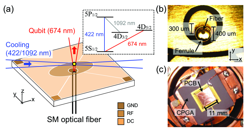
Fiber-trap integration is achieved by embedding the fiber within the trap substrate. Fig. 1(a) shows a schematic of the ion trap design, which is a modified version of the surface-electrode point Paul trap described recently Kim et al. (2010). The center, grounded electrode has a diameter of mm. The elliptical RF pad has major- and minor-axis diameters of mm and mm, respectively, and is shifted by m along the minor-axis relative to the center of the ground electrode. Electrode gaps are m. This design achieves an ion height of m and the electrode asymmetries uniquely define the principal axes of the trap, which are tilted by in the -plane for efficient cooling and micromotion compensation. The side electrodes are used for DC compensation of stray electric fields, as well as radial translation of the RF node by use of additional RF voltages. The trap is defined on a printed circuit board (PCB) with copper electrodes on a low-RF-loss substrate (Rogers 4350B, fabricated by Hughes circuits). The PCB includes a m-diameter plated via in the center ground electrode for the insertion of an optical ferrule. The via is offset by m with respect to the ground electrode to account for the displacement of the trapping point that accompanies the shift of the elliptical RF electrode.
The optical fiber (OZ Optics, PMF-633-4/125-3-L) is SM for nm and is conventionally prepared (i.e. cured in fiber epoxy and polished) in a stainless steel SMA ferrule whose tip has been machined to match the m-diameter of the PCB via. The assembly of PCB and ferrule is performed under microscope, as in Fig. 1(b), where machining imprecision of the ferrule is evident in the form of m nonconcentricity between the fiber and the ferrule. The ferrule is rotated with respect to the PCB to place the fiber roughly along the minor axis of the trap, and is cured using cyanoacrylate adhesive.
The fiber-trap system is installed on a ceramic pin grid array (CPGA) and mounted on the K baseplate of a closed-cycle cryostat Antohi et al. (2009) as shown in Fig. 1(c). The fiber is routed through a hole in the CPGA and a hole in a flange of the vacuum chamber, where it is sealed in place with TorrSeal UHV epoxy. The trap is operated at a typical RF frequency of MHz and Vpp amplitude, achieving secular frequencies of kHz, kHz, kHz. We produce 88Sr+ ions by resonant photoionization Brownnutt et al. (2007), which are Doppler cooled on the S1/25P1/2 transition at nm, while simultaneously driving the 4D3/25P1/2 transition at nm. Ion fluorescence at nm is collected by a NA lens inside the chamber and imaged onto a CCD camera and a photomultiplier tube (PMT), both with individual ion resolution.
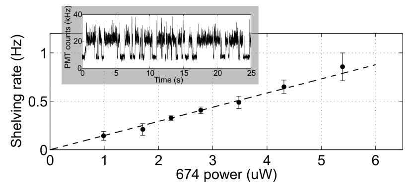
Interaction between the ion and the fiber mode is demonstrated using the electron shelving method Dehmelt (1975). The ion is driven on the 5S1/24D5/2 transition by nm light from the fiber while being simultaneously illuminated by the nm and nm beams. Upon shelving to the 4D5/2 state, no nm photons are scattered and the ion remains dark until it decays spontaneously back to the 5S1/2 state, as illustrated by the single-ion telegraph in the inset of Fig. 2. An effective shelving rate can be quantified by counting the bright-to-dark transitions per total bright time. In Fig. 2, the linear relationship between shelving rate and nm power coupled to the fiber is shown, as expected for a weak driving field.
Because of the exponential fall-off in intensity along the transverse plane of a Gaussian mode, a method for in situ control of the ion positioning is highly desired. While DC potentials may achieve ion translation, the resultant displacement of the ion from the RF node incurs additional micromotion that broadens atomic transitions Berkeland et al. (1998), which significantly limits the range and usefulness of DC translation. In contrast, micromotion-free translation can be achieved by shifting the quadrupole field node itself, as has been demonstrated recently Herskind et al. (2009b); VanDevender et al. (2010); Kim et al. (2010), by using multiple RF-voltages applied to different electrodes of the trap.
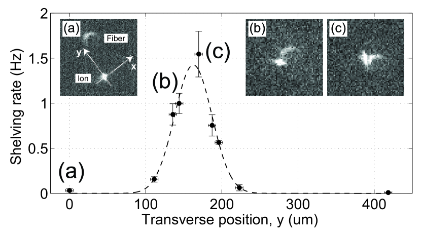
We utilize multiple RF sources to achieve micromotion-free translation of the ion in the horizontal plane of a surface-electrode ion trap. Fig. 3 shows the change in shelving rate as the ion is translated along the -axis, across the mode of the fiber. The dashed line represents a Gaussian beam shape indicating good qualitative agreement with the shelving rate profile. The beam waist at the ion height of m has been measured independently using an identical fiber to be m, which is used to calibrate the -axis in Fig. 3. In units of the measured mode waist, the ion is brought to within of the mode center, despite an initial displacement of arising from trap construction. CCD images show the ion displaced relative to the (unfocused) image of the fiber. In all measurements, the ion was positioned at the RF node by eliminating micromotion amplitude according to the correlation measurement technique Berkeland et al. (1998).
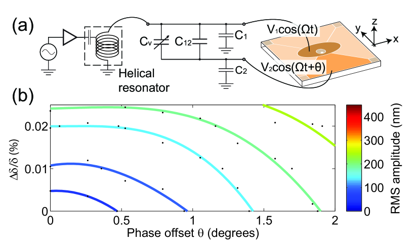
The ultimate precision of RF translation is limited by the stability and control of the relative amplitudes and phases between the multiple sources. The position uncertainty indicated in Fig. 3 is limited by the resolution of our imaging system to m and is not fundamental to the RF node translation method. Fig. 4(a) shows our implementation for achieving two in-phase RF voltages through a passive network. Capacitances pF are intrinsic to the trap electrodes and cryostat wiring, as is pF, which accounts for the intrinsic capacitive coupling between the two electrodes. We introduce a mechanically tunable capacitor pF (Voltronics Corp.) in order to adjust the RF ratio . Fig. 4(b) is the results of a Monte Carlo simulation at the operational point (c) of Fig. 3, showing RMS amplitudes of classical ion trajectories in steps of nm under RF ratio () and phase () imperfections. Given a typical temperature coefficient of ppmC∘ for we expect a ratio imprecision of C∘, while phase error arises from differential resistances of the two wire paths at a negligible per differential ohm. With a C control in capacitor temperature, we conclude that the current implementation achieves nm RMS positioning precision. Furthermore, the sensitivity to RF imperfections is trap-design dependent, and may be reduced at the cost of total translational range.
With the ion centered in the fiber mode, we have looked for effects of dielectric charging by the nm fiber light Harlander et al. (2010). In these tests, W of nm light is coupled into the fiber while the amplitude of ion micromotion is recorded for several minutes to detect any dynamic shifts in the ion position due to a possible fiber-induced generation of charge. We observe induced fields of V/m by the fiber, with charging and discharging time constants of s and s. Following the initial charge generation, the micromotion amplitude remains constant for minutes, indicating stable saturation of fiber-induced charge.
In conclusion, we have demonstrated an ion trap with an integrated SM fiber for light delivery, and an in situ micromotion-free optimization of the ion-fiber spatial overlap. The fiber has been used to directly address the qubit transition of a single ion in the trap and, as such, the fiber-trap system represents a step towards optics-integration for large-scale QIP in surface-electrode designs. Moreover, our assembly is compatible with more advanced fiber systems, such as lensed fibers to achieve higher field intensities, or photonic crystal fibers that propagate all relevant lasers through a single integrated port. In a cryogenic environment, such an all-inclusive port may eliminate the requirement of free-space optical access, greatly reducing the heatload and enabling sub-Kelvin trap operation. An integrated trap that utilizes the fiber facet as one of the mirrors of an optical cavity could serve as a node in a distributed QIP architecture where the photon state can be extracted through the fiber Cirac et al. (1997); Kim and Kim (2009).
Acknowledgements.
T.H.K. was supported by the Siebel and Chorafas Foundations. P.F.H. is grateful for the support from the Carlsberg and Lundbeck Foundations.References
- Cirac et al. (1997) J. I. Cirac, P. Zoller, H. J. Kimble, and H. Mabuchi, Physical Review Letters 78, 3221 (1997).
- Kim et al. (2005) J. Kim, S. Pau, Z. Ma, H. R. McLellan, J. V. Gates, A. Kornblit, R. E. Slusher, R. M. Jopson, I. Kang, and M. Dinu, Quantum Information & Computation 5, 515 (2005).
- Harlander et al. (2010) M. Harlander, M. Brownnutt, W. Hansel, and R. Blatt, New Journal of Physics 12, 093035 (2010).
- Guthohrlein et al. (2001) G. R. Guthohrlein, M. Keller, K. Hayasaka, W. Lange, and H. Walther, Nature 414, 49 (2001).
- Herskind et al. (2009a) P. F. Herskind, A. Dantan, J. P. Marler, M. Albert, and M. Drewsen, Nature Physics 5, 494 (2009a).
- Shu et al. (2010) G. Shu, N. Kurz, M. Dietrich, and B. B. Blinov, Phys. Rev. A 81, 042321 (2010).
- Wilson et al. (2011) A. Wilson, H. Takahashi, A. Riley-Watson, F. Orucevic, P. Blythe, A. Mortensen, D. R. Crick, N. Seymour-Smith, E. Brama, M. Keller, and W. Lange, arXiv:1101.5877 (2011).
- Streed et al. (2011) E. W. Streed, B. Norton, A. Jechow, T. J. Weinhold, and D. Kielpinski, Phys. Rev. Lett. 106, 010502 (2011).
- VanDevender et al. (2010) A. P. VanDevender, Y. Colombe, J. Amini, D. Leibfried, and D. J. Wineland, Physical Review Letters 105, 023001 (2010).
- Herskind et al. (2010) P. F. Herskind, S. X. Wang, M. Shi, Y. Ge, M. Cetina, and I. L. Chuang, arXiv:1011.5259v1 (2010).
- Kim and Kim (2009) J. Kim and C. Kim, Quantum Information & Computation 9, 0181 (2009).
- Schneider et al. (2010) C. Schneider, M. Enderlein, T. Huber, and T. Schaetz, Nature Photonics 4, 772 (2010).
- Herskind et al. (2009b) P. F. Herskind, A. Dantan, M. Albert, J. P. Marler, and M. Drewsen, Journal Of Physics B 42, 154008 (2009b).
- Blatt and Wineland (2008) R. Blatt and D. J. Wineland, Nature 453, 1008 (2008).
- Margolis et al. (2004) H. Margolis, G. Barwood, G. Huang, H. A. Klein, S. Lea, K. Szymaniec, and P. Gill, Science 306, 1355 (2004).
- Kim et al. (2010) T. H. Kim, P. F. Herskind, T. Kim, J. Kim, and I. L. Chuang, Phys. Rev. A 82, 043412 (2010).
- Antohi et al. (2009) P. B. Antohi, D. Schuster, G. M. Akselrod, J. Labaziewicz, Y. Ge, Z. Lin, W. S. Bakr, and I. L. Chuang, Rev. Sci. Instrum. 80, 013103 (2009).
- Brownnutt et al. (2007) M. Brownnutt, V. Letchumanan, G. Wilpers, R. C. Thompson, P. Gill, and A. G. Sinclair, Applied Physics B-Lasers And Optics 87, 411 (2007).
- Dehmelt (1975) H. Dehmelt, Bulletin of the American Physical Society 20, 60 (1975).
- Berkeland et al. (1998) D. J. Berkeland, J. D. Miller, J. C. Bergquist, W. M. Itano, and D. J. Wineland, Journal Of Applied Physics 83, 5025 (1998).