Blowing of Polysilicon Fuses
Abstract
Polysilicon fuses are one time programmable memory elements which allow the calibration of integrated circuits at wafer and package level. We present a zero dimensional lumped parameter model of the programming of fuses made from a combination of tungsten silicide and polycrystalline silicon. The components of the model are an electrical model, a thermal model and a flow model. The electrical model describes the temperature and geometry dependent resistance of the fuse. The thermal model describes the heating and melting of the fuse and its surroundings. The flow model describes the disconnection of the fuse by electromigration driven flow of silica. The model generates quantitatively accurate results and reproduces trends with applied voltage and fuse size.
pacs:
84.32.Vv 66.30.QaPolysilicon fuses are one time programmable memory elements in silicon chips. They are utilised as permanent on chip memory storage for calibration factors in precision analogue circuits and can be programmed (blown) at both wafer and package levels. Polysilicon fuses are constructed from layers of polycrystalline silicon (polysilicon) and metal silicides. Theories of the blowing process which have been put forward invoke grain recrystallisation Tonti2003 , melting and vapourisation Li2006 and electromigration Doorn2007 .
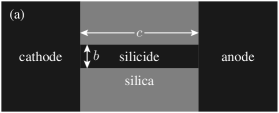
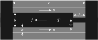
One fuse design is shown in Figure 1. The fuse is completely solid state and consists of layers of conducting tungsten silicide and semiconducting polysilicon surrounded by insulating silica. The thickness of the polysilicon and tungsten silicide layers are and respectively, the width of the fuse is and its length is . The electrodes on either side of the fuse are made from the same materials with the same thickness but are much larger in the other two directions.
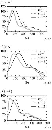
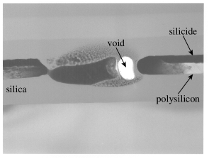
The fuse is blown by the application of a fixed potential bias across the fuse. Current versus time graphs are shown for different voltages and different size fuses in Figure 2. The microstructure of a blown fuse is shown in Figure 3. The following features of the blowing process are apparent: (i) there is evidence of melting of the fuse, and of parts of the electrodes and the silica surrounding the fuse; (ii) the fuse is disconnected by both a void and by a layer of silica. A model of the fuse blowing process must explain these observations.
We propose that the fuse blowing process occurs by the following steps. (1) When the current starts to flow, it flows mostly through the metallic silicide. As the fuse heats up, the silicide conductivity reduces but the conductivity of the semiconducting polysilicon increases until it is the dominant conductor. The overall effect is that the conductivity of the fuse first increases then decreases. (2) Eventually the fuse, parts of the electrodes and some of the silica surrounding the fuse melt. (3) Electromigration drives the fuse material towards the cathode. This displaces the insulating molten silica towards the anode, where it begins to pinch off the fuse from the anode. (4) When pinch off is nearly complete the fuse ruptures forming the void (this process is driven by the contraction of silicon on melting).
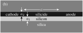
To model the fuse blowing process we use a lumped parameter approach. This model builds on work reported in Ref. esgi62, . The lumped parameter model of the fuse consists of ordinary differential equations for the temperature, , of the fuse, and the height, , and width, , of the pinched off region. These variables are illustrated in Figure 4. An electronic model describes the temperature and geometry dependent resistance of the fuse; a thermodynamic model describes the heating and melting of the fuse and its surroundings; a flow model describes the electromigration driven pinch off of the fuse. The rupture of the fuse is not modelled explicitly: it is assumed that rupture occurs just as pinch off is complete.
Electronics
Electrically the system consists of the fuse in series with a transistor. The fuse blowing process is initiated by a decrease of the transistor resistance from a very large value to . This decrease occurs on a nanosecond timescale and is assumed to be instantaneous in the model. The fuse can be modelled as two resistors in series, with a total resistance . The first resistor represents the part of the fuse unaffected by flow and has a temperature dependent resistance, . The second resistor represents the region of the fuse in which pinch off occurs and thus has a temperature and geometry dependent resistance, .
| (1) | ||||
| (2) |
The current flowing through the fuse is calculated from Ohm’s law.
Following Ref. Minixhofer2003, , conductivity, , is taken to be a quadratic function of temperature. There is insufficient data to separate out the contributions of the polysilicon and tungsten silicide layers, therefore a single conductivity function is used for both layers of the fuse.
| (3) |
As the fuse heats up, its conductivity increases until is reached and then it decreases.
Thermodynamics
The temperature, , of the fuse is assumed to be homogeneous throughout the fuse. The equation modelling its evolution is
| (4) |
The left hand side describes the heat capacity of the fuse. The terms on the right hand side describe Joule heating and Newtonian cooling respectively. is a the volume averaged heat capacity per unit volume of the fuse calculated from: and , the heat capacity per unit volume of polysilicon and tungsten silicide (assumed to be the same in the solid and liquid); and and , the enthalpies of fusion per unit volume of polysilicon and tungsten silicide. In solving the equations, the melting phase transitions (at and in polysilicon and tungsten silicide respectively) are assumed to have a finite width of . is the volume of the fuse, is the thermal conductivity of silica, is room temperature and is the surface area of the fuse, , is a thermal conduction length. A better fit to the data is obtained by allowing superheating of the tungsten silicide before it melts: this seems physically reasonable given the small size of the fuse and the rapid heating rates. Superheating is included within the model by increasing from its equilibrium value of .
Fluid mechanics
The body force driving electromigration is given by where is the charge density of charge carriers and is a constant of proportionality. The force acts on the conducting silicon and silicide and is directed from the anode to the cathode. The viscosities of the molten silicon and silicide are much lower than that of molten silica. Therefore flow is limited by the motion of silica. The electromigration body force sets up a pressure gradient within the fuse which is transmitted to the molten silica surrounding the fuse and causes it to move with a velocity where is the dynamic viscosity of molten silica and is the width of the molten silica region surrounding the fuse.
The equations describing the pinch-off of the fuse are
| (5) | ||||
| (6) |
The first equation expresses conservation of volume, the second is a crude balance between work done by body forces and work done against friction in the silica. Flow is only allowed to occur once has been exceeded. To allow the equations to be solved numerically and are initialised with small non-zero values.
The equations were solved numerically using a 4th order Runge-Kutta scheme with adaptive time-stepping. Parameter values used in the simulations are summarised in Table 1. The results are shown in Figure 2, for models using the equilibrium melting value of and the values including superheating given in Table 1. Considering the simplicity of the model the results are remarkably good and trends with voltage and fuse size are correctly predicted.
A zero dimensional, lumped parameter model of the programming of polysilicon fuses successfully reproduces the available experimental data for one type of fuse. The model captures trends with voltage and size. This strongly suggests that the assumptions used to construct the model are fundamentally correct. To take the model further, more experimental data are required, describing the temperature dependent conductivity of the individual polysilicon and tungsten silicide layers for example. This will allow three dimensional modelling of the partial differential equations describing the system.
| Parameter | Value | |
|---|---|---|
| 5 | ||
| 1700 | K | |
| 10 | Pa s | |
| 0.2 | ||
| 3.33 | ||
| 1400 | K | |
| 300 | K | |
| K | ||
| Property | (a) | (b) | (c) | |||
|---|---|---|---|---|---|---|
| V | V | V | ||||
| K | K | K | ||||
Acknowledgements.
We acknowledge support of the Mathematics Applications Consortium for Science and Industry (www.macsi.ul.ie) funded by the Science Foundation Ireland Mathematics Initiative Grant 06/MI/005.References
- (1) W. R. Tonti, J. A. Fifield, J. Higgins, W. H. Guthrie, W. Berry, and C. Narayan, 2003 IEEE International Integrated Reliability Workshop Final Report, 36(2003).
- (2) Y. J. Li and A. Tang, 2006 IEEE International Integrated Reliability Workshop Final Report, 194(2006).
- (3) T. S. Doorn, IEEE Transactions on Electron Devices 54, 3285 (2007).
- (4) M. J. Cooker, P. Dellar, W. T. Lee, C. deFalco, D. Barton, C. Farmer, A. Fowler, J. King, and G. I. Shiskin, “An investigation into the physics of blowing polysilicon fuses..” in 62nd European Study Group with Industry Reports (Smith Institute, 2008).
- (5) R. Minixhofer, S. Holzer, C. Heitzinger, J. Fellner, T. Grasser, and S. Selberher, Proceedings of the 33rd European Solid-State Device Research Conference, 363(2003).