, , , , , , , , , , , , , , , , , , , , , , , , , and ††thanks: Deceased. ††thanks: Present address: Institute for Nuclear Research, Russian Academy of Sciences, Moscow, Russia ††thanks: Corresponding author: Itzhak Tserruya E-mail: Itzhak.Tserruya@weizmann.ac.il
Design, Construction, Operation and Performance of a Hadron Blind Detector for the PHENIX Experiment
Abstract
A Hadron Blind Detector (HBD) has been developed, constructed and successfully operated within the PHENIX detector at RHIC. The HBD is a Cherenkov detector operated with pure CF4. It has a 50 cm long radiator directly coupled in a windowless configuration to a readout element consisting of a triple GEM stack, with a CsI photocathode evaporated on the top surface of the top GEM and pad readout at the bottom of the stack. This paper gives a comprehensive account of the construction, operation and in-beam performance of the detector.
keywords:
HBD , GEM , CsI photocathode , UV-photon detector , CF4PACS:
29.40.-n , 29.40.Cs , 29.40.Ka , 25.75.-q1 Introduction
We have developed a Hadron Blind Detector (HBD) as an upgrade of the PHENIX experiment at the Relativistic Heavy Ion Collider (RHIC) for the measurement of electron pairs, particularly in the low-mass region (m 1 GeV/c2). Low-mass dileptons are considered a powerful and unique probe to diagnose the hot and dense strongly interacting quark gluon plasma formed in ultra-relativistic heavy ion collisions [1]. They are sensitive to chiral symmetry restoration effects expected to take place in these collisions [2]. They can also be used to detect the thermal radiation emitted by the plasma via virtual photons providing a direct measurement of the plasma temperature, one of its most basic properties [3].
PHENIX is a large multipurpose experiment specially devoted to the measurement of rare probes, and electromagnetic probes in particular [4]. At mid-rapidity ( 0.35) the detector has excellent electron identification capabilities based on a RICH detector and an electromagnetic calorimeter. It also has a mass resolution of about 1% at the mass, which allows precision spectroscopy measurements of the light vector mesons and . The observation of spectral shape modifications of these mesons could provide direct information on the chiral symmetry restoration. However, the measurement of low-mass electron pairs in the original PHENIX detector configuration suffers from a huge combinatorial background, with a signal to background ratio of S/B 1/200 in the invariant dielectron mass range of m = 0.3-0.5 GeV/c2 [5]. The combinatorial background comes from the overwhelming yield of Dalitz decays and conversions and originates from the limited geometrical acceptance of the PHENIX detector (the central arm spectrometers consist of two arms each one covering the pseudo-rapidity interval 0.35 and 90o in azimuthal angle) and the very strong magnetic field starting at the vertex. Consequently, very often only one of the two tracks of an pair is detected in the central arm detectors. The second track never reaches the detectors (because it falls out of the acceptance or is curled by the magnetic field) or is not detected due to the inability to reconstruct low-momentum tracks with 200 MeV/c. These single tracks, when paired to other electron tracks in the same event, give rise to the combinatorial background.
The HBD aims at considerably reducing the combinatorial background from the two main background sources, Dalitz decays and conversions. The detector exploits the distinctive feature of the pairs from these two sources, namely their very small opening angle. The HBD is therefore located in a field free region that preserves the original direction of the pair. Electron tracks identified in the central arm detectors are rejected as likely partners of a Dalitz decay or a conversion pair if the corresponding hit in the HBD has a double amplitude or has a nearby hit within the typical opening angle of these pairs.
The HBD consists of a Cherenkov radiator that is directly coupled to a triple Gas Electron Multiplier (GEM) [6] detector with a CsI photocathode. Both the radiator and the GEMs are operated with pure CF4 in a common gas volume. The detector was constructed after extensive R&D to demonstrate the concept validity (see [7, 8] for the R&D results and [9, 10] for other previous reports related to the HBD).
This paper gives a comprehensive report on the design, construction, operation and performance of the HBD. The detector was commissioned in 2007 and has been fully operational since the fall of 2008. It was used as an integral part of the PHENIX detector in the RHIC runs of 2009 and 2010 which were devoted to the study of p+p collisions and Au+Au collisions, respectively. The paper is organized as follows: Section 2 presents the overall detector concept. The realization of the detector, including design, construction and test, is described in detail in Section 3. The detector services, including the readout electronics, the gas handling and monitoring system and the high voltage system are described in Sections 4, 5 and 6, respectively. The operation and monitoring of the detector under running conditions are presented in Section 7. Section 8 gives a comprehensive account of the detector performance. A short summary is provided in Section 9.
2 Detector concept
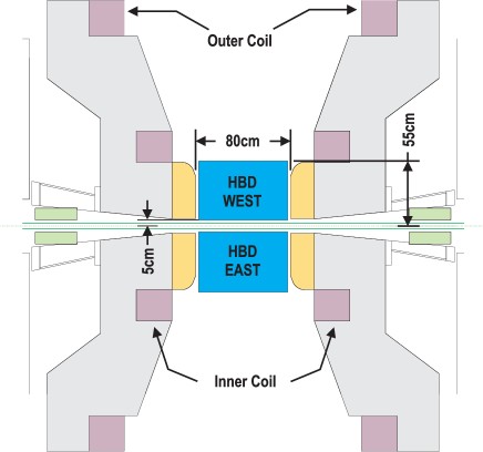
The main task of the HBD is to recognize and reject conversions and Dalitz decays. The strategy is to exploit the fact that the opening angle of electron pairs from these sources is very small compared to the pairs from light vector mesons. In a field-free region, this angle is preserved and by applying an opening angle cut one can reject more than 90% of the conversions and Dalitz decays, while keeping most of the signal. The PHENIX central arm magnetic field consists of an inner and outer coil that can be operated independently. The field free region, necessary for the operation of the HBD, is generated by allowing the current in these two coils to flow in opposite directions. In this so-called “” mode, the inner coil located at a radius of 60 cm counteracts the action of the outer coil resulting in an almost field free region extending out to 50-60 cm in the radial direction. The size of the HBD is constrained by the available space in the field free region, from the beam pipe (at r 5 cm) up to the location of the inner coil. Fig. 1 shows the layout of the inner part of the PHENIX detector together with the location of the coils and the HBD.
The system specifications of the HBD were defined by Monte Carlo simulations performed at the ideal detector level aiming at reducing the combinatorial background originating from conversions and Dalitz decays by two orders of magnitude. At this level of rejection, the quality of the low-mass pair measurement is no longer limited by the background originating from these sources, but rather by the background originating from the semi-leptonic decay of charmed mesons. The simulations showed that the goal can be achieved with a detector that provides electron identification with an efficiency of 90%. This also implies a double electron hit recognition at a comparable level. The separation between single and double electron hits is one of the main performance parameters of this detector. On the other hand, a moderate hadron rejection factor of 50 is sufficient. It is also important to have a larger acceptance in the HBD compared to the fiducial central arm acceptance to provide a veto area for the rejection of pairs where only one partner is inside the fiducial acceptance.
The requirements on electron identification limit the choice to a Cherenkov-type detector. In order to generate enough UV photons in a 50 cm long radiator to ensure good distinction between single and double hits, we adopted a windowless scheme without mirror and chose pure CF4 as radiator and detector gas. The use of a UV transparent window between the radiator and the detector element and of a mirror, as commonly done in RICH detectors, limits the bandwidth to about 8-9 eV. The choice of CF4 both as the radiator and detector gas in a windowless geometry results in a very large bandwidth (from 6 eV given by the threshold of CsI to 11.1 eV given by the CF4 cut-off) and consequently a very large figure of merit N0. The N0 value is estimated to be close to 700 cm-1 under ideal conditions with no losses. The large value of N0 ensures a very high electron efficiency, and more importantly, is crucial for achieving good double-hit resolution.
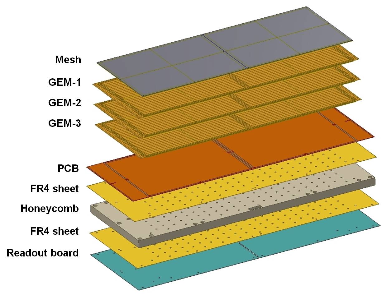
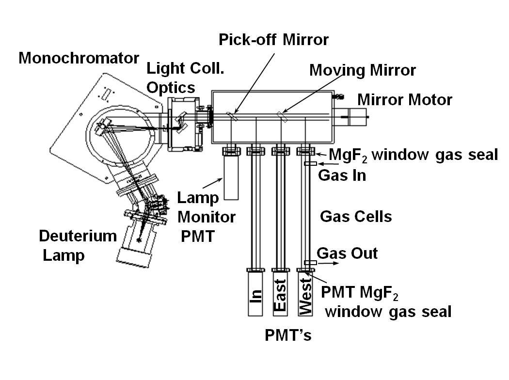
In this windowless proximity focus configuration, the Cherenkov light from particles passing through the radiator is directly collected on a photosensitive cathode plane, forming an almost circular blob image rather than a ring as in a conventional RICH detector. After consideration of relevant options, we chose a triple GEM detector with a CsI photocathode evaporated on the top surface of the first GEM foil as the active detector element. The signal is collected by a pad readout at the bottom of the GEM stack (see Fig. 2). In this reflective photocathode scheme, the photoelectrons are pulled into the holes of the GEM by the strong electric field inside the holes and the photocathode is totally screened from photons produced in the avalanche process.
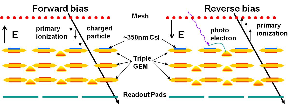
The hadron blindness property of the HBD is achieved by operating the detector in the so-called reverse bias mode as opposed to the standard forward bias (FB) mode (see Fig. 2). In the reverse bias (RB) mode, the mesh is set at a lower negative voltage with respect to the GEM and consequently the ionization electrons deposited by a charged particle in the drift region between the entrance mesh and the top GEM are mostly repelled towards the mesh (see Fig. 2 right panel). Consequently, the signal produced by a charged particle results only from (i) the collection of ionization charge from only a thin layer of m above the top GEM which is subject to the entire 3-stage amplification, and (ii) the collection of ionization charge in the first transfer gap (between the top and the middle GEMs) which is subject to a 2-stage amplification only. The ionization electrons produced in the second transfer gap and in the induction gap generate a negligible signal since they experience one and zero stages of amplification, respectively. For a drift region and a transfer gap of 1.5 mm each and a total gas gain of 5000, the mean amplitude of a hadron signal drops to of its value in the forward bias mode [8].
The readout pad plane consists of hexagonal pads with an area of 6.2 cm2 (hexagon side length a = 1.55 cm) which is comparable to, but smaller than, the blob size which has a maximum area of 9.9 cm2. Therefore, the probability of a single-pad hit by an electron entering the HBD is very small. On the other hand, a hadron traversing the HBD will produce a signal predominantly localized in a single pad. This provides an additional strong handle in the hadron rejection of the HBD.
The relatively large pad size also results in a low granularity thereby reducing the cost of the detector. In addition, since the signal produced by a single electron is distributed between 2-3 pads, one expects a primary charge of several photoelectrons per pad, allowing the operation of the detector at a relatively moderate gain of a few times 103. This is a crucial advantage for stable operation of a UV photon detector.
3 HBD design, construction, and testing
3.1 Design overview
The detector design derives from the system specifications and the space constraints discussed in Section 2. In addition, special care was taken to minimize (i) the amount of material in order to reduce as much as possible the number of photon conversions in the central arm acceptance and (ii) the dead or inactive areas due to frames or spacing between adjacent detector modules in order to achieve the highest possible efficiency. Table 1 summarizes the most important design parameters.
| Acceptance | 0.45 =135o |
|---|---|
| GEM size () | 23 27 cm2 |
| GEM supporting frame and cross (w x d) | frame: 51.5 mm2, cross: 0.31.5 mm2 |
| Hexagonal pad side length | a = 15.5 mm |
| Number of pads per arm | 1152 |
| Dead area within central arm acceptance | 7% |
| Total Radiation length within central arm acceptance | 2.40% |
| Weight per arm (including HV and gas connectors) | 10 kg |
The HBD is made of two identical arms, located close to the interaction vertex. The entrance window is located just after the beam pipe at r5 cm. The detector extends to r60 cm in the radial direction and 65.5 cm along the beam axis (see Fig. 1 and Fig. 3 left panel). Each arm covers 135o in azimuthal angle and 0.45 units in pseudorapidity . This extended acceptance with respect to the central arms (which cover 90o in and 0.35 units in ) provides a very generous veto area for efficient rejection of close pairs where only one track falls inside the fiducial acceptance.
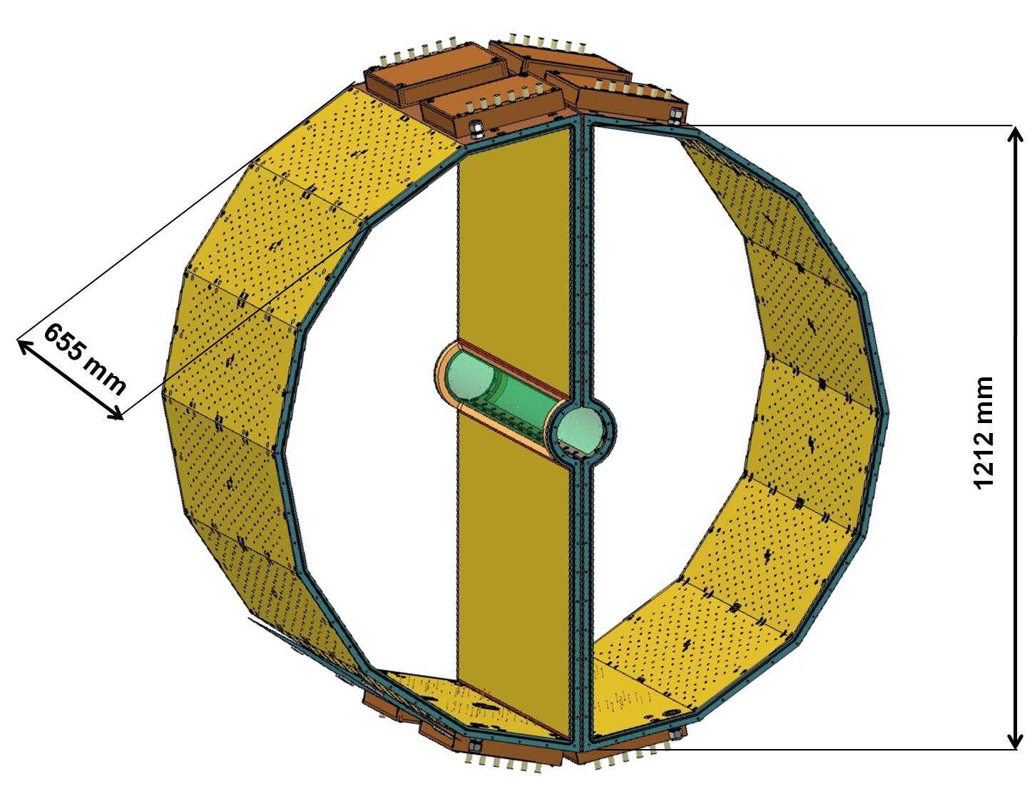
The right panel of Fig. 3 shows an exploded view of one HBD arm, displaying the various elements of the detector. Each arm consists of a 50 cm long radiator directly coupled to a triple GEM photon detector. The latter is subdivided in 12 detector modules, 6 along the axis 2 along the z axis. With this segmentation, each detector module is 23 27 cm2 in size. In the 2009 and 2010 RHIC runs, 10 modules were instrumented in each arm covering an azimuthal range of 112.5o which is considerably larger than the azimuthal range of 90o covered by the central arm detectors.
3.2 Detector vessel
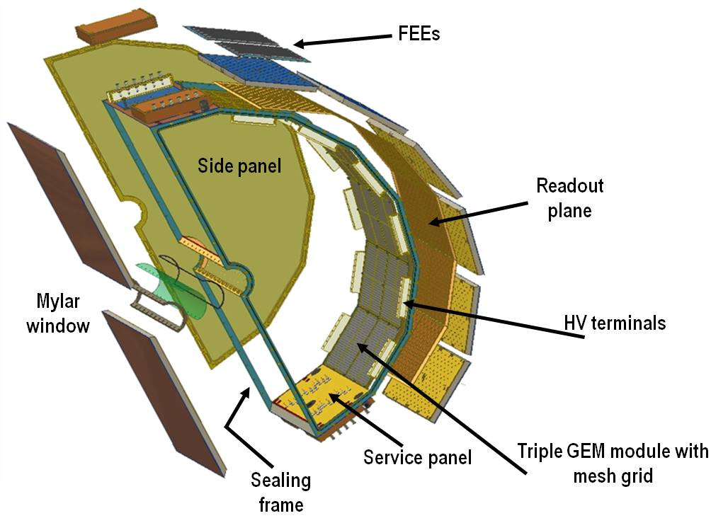
The detector vessel has a polygonal shape formed by panels glued together as shown in Fig. 3. Eight panels of 63.0 23.7 cm2 and two vertical panels of 63.0 54.8 cm2 define the polygonal shape. The panels consist of a 19 mm thick honeycomb core sandwiched between two 0.25 mm thick FR4 sheets. Six of the eight panels define the HBD active area. The other two panels, outside the active area, are service panels. Gas-in and gas-out connections, HV connectors serving the GEMs, and a small UV-transparent window are located on these two panels.
Two supporting frames made of FR4, 19 mm thick (dictated by the thickness of the honeycomb core of the panels) and 7 mm wide, connect all panels together on each side providing mechanical stability and rigidity to the entire box. A thin window around the beam pipe is used to further reduce the radiation length in the HBD fiducial acceptance. The window is made of a 50 m thick layer of aclar and a 25 m thick layer of black kapton on the inside to minimize reflections. It is glued on a semi-cylindrical FR4 frame bolted to the supporting frame along the beam axis and is therefore easily removable. The two sides of the box are closed with covers made of 12.5 mm thick honeycomb core sandwiched between two 0.25 mm thick FR4 facesheets that are bolted on the supporting frame with an o-ring seal. Each side panel also has a 12.5 mm thick (dictated by the thickness of the honeycomb core of the side covers) and 15 mm wide frame around its perimeter to provide rigidity in the bolting area.
Fig. 4 presents an exploded view of a single back-side panel, showing the various components of one HBD panel (two detector modules) and the readout board attached to it. The mesh and the three GEM foils are mounted on FR4 fiberglass frames. The frames have a width of 5 mm and a thickness of 1.5 mm that defines the intergap distance. To prevent sagitta of the foils in the electrostatic fields, the frames have a supporting cross (0.3 mm thick) in the middle. The three GEM foils and the mesh are stacked together and attached to the detector vessel by 8 pins. These pins, located at the corners and the middle of the frame, keep the tension on the GEM foils and the mesh while maintaining a minimum deformation of the 5 mm wide frames. Special tooling was developed to stretch the foils and the mesh and to glue them onto the narrow frames. The design allows for only 1 mm clearance between two adjacent detectors. With this design, the resulting total dead area within the central arm acceptance is calculated to be 7%.
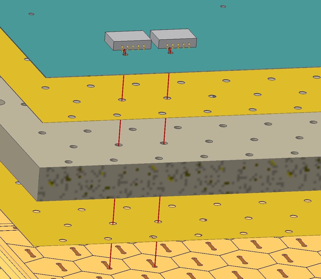
The detector anode is a double-sided printed circuit board (PCB) with a hexagonal pad pattern on the inner side and short signal traces (seen at the bottom of Fig. 5) on the other side. The side length of the hexagonal pads is a = 15.5 mm resulting in 96 pads in each detector module and a total of 1152 pads in each arm. Plated-through holes in the PCB connect the pads to the signal traces. Short wires are soldered at the edges of these traces (1.5 cm from the plated-through holes), passed through small holes in the panels and soldered to traces on the readout board located outside the detector that carry the signals to the preamplifiers (see Fig. 5). The PCB is made of 50 m thick kapton foil with 5 m copper cladding, in one single piece (140 63 cm2). The PCB is glued onto the eight panels which define the outside polygonal shape of the detector vessel (see Fig. 3).
Special attention was taken in the design to ensure gas tightness of the detector vessel. The plated-through holes are effectively sealed by the panels that are glued on the back side of the PCB. Making the PCB in one piece and gluing it to the panels behind prevents any potential leaks at the junctions between adjacent panels. The junctions between adjacent panels of the vessel are easily sealed by gluing a 50 m thick kapton strip along the inner side of the junction. The leak rate in each vessel, which has a total volume of 313 l, was measured to be 0.12 cc/min.
Each detector vessel alone weighs 5 kg and adding all other components (HV connectors, gas in/out, GEM foils, preamplifier cards…) results in a total weight of less than 10 kg per arm. The total radiation length of the detector vessel within the central arm acceptance is calculated to be 0.82%. To this, one must add the contribution of the readout board and pre-amps that is attached to the vessel (estimated to be 1.03%) and the 50 cm CF4 radiator gas (estimated to be 0.56%) to give a total of 2.4 % of a radiation length for the entire detector. The material budget is itemized in Table 2.
| Component | Material | X0 (cm) | Thickness (cm) | Area () | Rad. Length (%) |
| Vessel | |||||
| Window | Aclar/kapton | 15.8/28.6 | 0.0075/0.0050 | 100 | 0.040 |
| Mesh | SS | 1.67 | 0.003 | 11.5 | 0.021 |
| GEM | Kapton | 28.6 | 0.0053 | 64 | 0.034 |
| GEM | Copper | 1.43 | 0.00056 | 64 | 0.134 |
| GEM frames | FR4 | 17.1 | 0.154 | 6.5 | 0.228 |
| PCB | Kapton | 28.6 | 0.005 | 100 | 0.017 |
| PCB | Copper | 1.43 | 0.0005 | 80 | 0.028 |
| Facesheet | FR4 | 17.1 | 0.0252 | 100 | 0.292 |
| Panel core | Honeycomb | 8170 | 1.905 | 100 | 0.023 |
| Total vessel | 0.82 | ||||
| Readout | |||||
| Readout board | FR4/copper | 17.1/1.43 | 0.05/0.001 | 100 | 0.367 |
| Preamps + sockets | Copper | 1.43 | 0.0005 | 100 | 0.66 |
| Total readout | 1.03 | ||||
| Gas | CF4 | 9240 | 51.5 | 100 | 0.56 |
| Total | 2.4 |
3.3 GEM electrodes
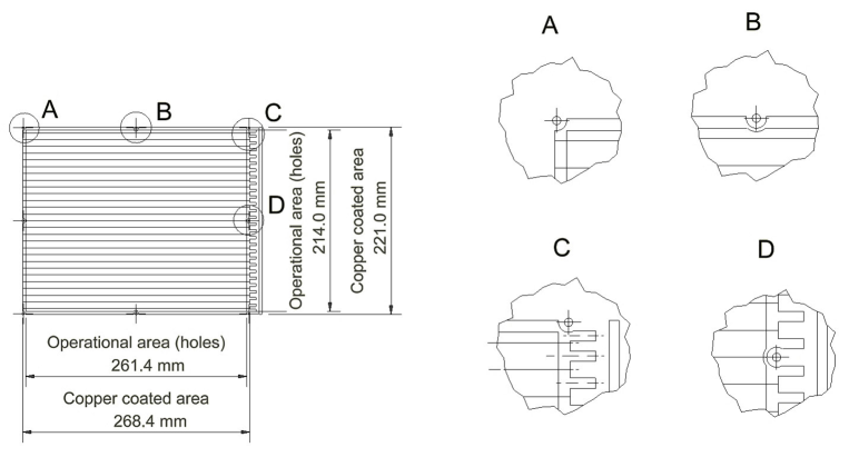
The GEMs for the HBD were all produced at the Technical Support Department at CERN. Each GEM is made of a 50 m thick, metal-clad (5 m thick copper on each side) polymer foil commonly known as kapton. It is chemically etched to produce a highly dense pattern of 60-80 m diameter holes with 140 m pitch. The copper coated area of the foils is 268.4 221 mm2, whereas the operational area i.e. the area with holes is 261.4 214 mm2. The top face of each GEM foil is divided into 28 high voltage segments: 26 central segments of 8 mm each and a first and last segment of 6.5 mm. The gap without copper between the segments is 200 m. Fig. 6 gives the detailed geometry of the GEM foils, showing the various dimensions.
All GEM foils were electrically tested at CERN prior to shipping to the Weizmann Institute. The tests were done in a clean room in dry air (30 humidity). The foils were accepted if the leakage current was below 5 nA at 600 V.
Upon arrival at the Weizmann Institute the foils were again electrically tested before framing. The test was done in air, either in a clean room or on a laminar flow table. HV was applied on the top surface of the GEM foil to each of the 28 strips with the bottom surface grounded. Since the humidity in the test area was not as low at it was during the initial test at CERN the voltage was raised up to only 550 V. However, the criteria for accepting a good foil was the same as it was at CERN, namely less than 5 nA of leakage current. A few foils exhibited a high current or even a short during testing. The foils which showed high leakage current were gently blown with clean and dry compressed nitrogen in order to remove any residual dust that could cause the high leakage current. If after this cleaning procedure the foil still showed high leakage current it was rejected. However, this happened very rarely.
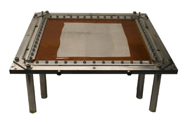
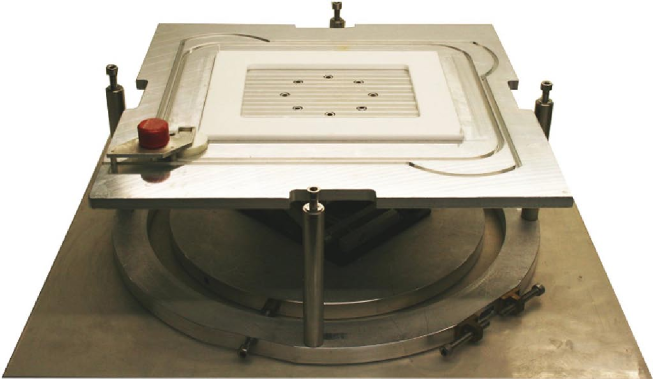
After passing the HV test the foils are ready to be glued on FR4 frames. The frames are 5 mm wide and with inner dimensions of 263.4 216.0 mm2 so that the ”dead” area of the foil, i.e. the area without holes, is 1 mm wide along the inner sides of the frame. This 1 mm spacing prevents glue from filling the holes during framing. First the foils are stretched using a custom designed stretching fixture (see Fig. 7). The 400 400 mm2 foil is placed inside L-shaped frames along each of the four sides, covered with aluminum bars and tightened down with a set of screws. The foil is then stretched using two bolts on each of the four sides of the frame to equally distribute the tension across the foil.
After stretching, the foil is carefully aligned with respect to the FR4 frame in order to match the eight mounting holes in the foil to those in the frame, using a positioning device which also serves as glue dispenser (see Fig. 8). The latter consists of a rigid base on which a small lifting table is mounted that contains a large plate the size of the foil. The FR4 frame is mounted on top of this plate together with a Teflon frame and eight Teflon pins that protrude several mm. The stretching device together with the stretched foil is then mounted a few millimeters above the positioning device for the hole alignment. The positioning device allows for a fine adjustment of the position of the large plate. Once the holes are aligned, the stretching device is momentarily removed to apply glue to the FR4 frame. A custom designed glue dispenser moves along a grove on the plate and deposits a uniform layer of glue of 100 m thickness onto the FR4 frame. The glue used is Araldite AY103 epoxy with HY991 hardener mixed in a proportion of 100:40 by weight. The glue is pumped prior to use in a desiccator in order to remove residual air bubbles and had to be applied within about one hour after mixing with full polymerization taking approximately 16 hours at 30-35oC. After applying the glue, the stretching device together with the stretched foil is brought back to the positioning device. After verifying the alignment, the lifting table is raised in order to bring the FR4 frame in contact with the foil. The assembly is then fixed and allowed to cure for typically 24 hours.
The foils are then cut and removed from the stretching frame. First, a rough cut is made around the FR4 frame using a scalpel (Fig. 7 shows the remaining part of the foil after this cut). Then a precise cut, very close to the frame, is made in order to remove the remaining Kapton. The foil is then cleaned by gently blowing it with clean dry nitrogen. Another electrical test is performed by raising each high voltage strip to 550 V in air as had previously been done. In some rare cases, some foils do not pass the acceptance criteria of less than 5 nA of leakage current. These foils are then washed with deionized water, rinsed with alcohol, blown dry and tested again. This process is sometimes repeated two times. If the leakage current still exceeds our limit after the second trial, the foil is rejected.
GEMs that pass the high voltage tests then have 20 M surface mounted resistors installed on each high voltage segment. When soldering these resistors, the GEM is placed inside a Plexiglas box such that only the soldering pads for the resistors protrude out for soldering in order to protect the active area of the GEM foil. After soldering the resistors, the foils are again tested up to 550 V as a final high voltage test before shipping them off to Stony Brook University for assembly into the HBD vessel.
3.4 Assembly and testing
3.4.1 GEM storage prior to assembly
To ensure a dust and water-free environment, GEMs that arrive at Stony Brook are stored under high vacuum. A turbo-molecular pump is used to generate vacuum in the low Torr range. Prior to insertion in vacuum, each GEM is further washed and tested.
GEMs are gently sprayed with deionized water for 30 seconds, followed by a rinse with clean isopropyl alcohol. The GEMs are then blown dry with compressed gas that was passed through a gas ionizer to facilitate removal of any dust particles. The GEMs are then placed in high vacuum for 24 hours to ensure removal of all moisture from the kapton and FR4 frames. GEMs that contain moisture are found to have large leakage currents (on the order of a few A at dV = 100 V). This washing process is repeated on any GEMs which develop anomalously high leakage current and successfully recovers 30% of these GEMs.
After drying in vacuum, each GEM is moved to a high voltage test station on a laminar flow table with an ISO Class 1 atmosphere. Three electrical tests are then performed in air:
-
1.
The leads of each GEM are checked to have continuity to the top or bottom of the GEM. This is most easily tested by confirming the capacitance of the GEM through the leads with a hand-held multimeter.
-
2.
Each individual strip on the top side of the GEM is tested for continuity through the resistors to the HV input trace. With the bottom of the GEM grounded, the top side of the GEM is raised to -100 V. A voltage probe is used to determine that the proper voltage is present on each of the 28 strips on the top side of the GEM. During this process, the leakage current is carefully monitored. GEMs drawing less than 5 nA are accepted.
-
3.
High voltage is finally applied to the GEM to monitor stability and leakage current. A current limit of 1 A is set on the power supply to limit damage to the GEM in the event of a discharge. With the bottom side of the GEM grounded, the top side is slowly brought to 550 V. GEMs that are stable and have leakage currents less than 5 nA are accepted. GEMs which initially display moderately high leakage currents (10-500 nA), but no discharges, are left at voltage for up to an hour. Often the current falls back into the acceptable range.
GEMs that pass these tests are returned to high vacuum for storage, while those that fail are rewashed and tested again. GEMs which continue to fail after two cycles of washing are not used in the HBD.
3.4.2 Copper GEM assembly
All GEMs are dust sensitive and must be handled in a clean room or (preferably) upon a laminar flow table. Once coated with CsI, the devices are also water sensitive and will lose their quantum efficiency if exposed to an atmosphere with high water concentration for an extended period of time. For this reason, CsI-coated photosensitive GEMs are handled in the inert atmosphere of a glovebox. Unfortunately, since a glovebox is a closed-loop system it cannot maintain the level of cleanliness found on the laminar table. Because of this, strategies that minimize handling of the HBD (and GEMs) in the glovebox were found to produce the best results. The most successful procedure for HBD assembly involved assembling the bottom two layers of all GEM stacks in the cleanest available environment (the laminar flow table), and then adding the CsI-coated GEMs in the dry glovebox environment. This procedure limited exposure to the glovebox environment to 2-3 weeks.
For installation of the Cu GEMs, the HBD vessel is mounted on a rotating fixture and placed in front of the laminar flow table. With clean air blowing through the interior of the vessel, the standard copper GEMs (two per module) are mounted in place over the readout pads as shown in Fig. 9. After mounting, each GEM is re-tested in situ for continuity and stability (tests no. 1 and 3 above) to ensure no damage was caused during installation.
Once all standard GEMs are installed and re-tested, the vessel is moved into a sealed glovebox to accept the CsI-coated gold GEMs at the top of the triple-GEM stack. Once sealed, the glovebox recirculates nitrogen through a purifier and achieves H2O concentrations of 10 ppm. Regular sweeps of the interior of the glovebox with an ULPA vacuum cleaner mounted inside the glovebox atmosphere ensure that particulate contamination is at an acceptable level.
One critical choice for the glovebox was the selection of the material of the gloves themselves. While Butyl gloves provide the best water barrier, they are not highly rated with regard to generation of particulate matter. Hypalon gloves were selected as having the best rating for particulate matter, and were found to elevate the baseline water concentration of an empty glovebox from 2-3 ppm to 7-8 ppm, which was still quite acceptable.
3.4.3 Evaporation of CsI onto Au plated GEMs
GEMs are made photosensitive by the evaporation of a thin layer of CsI on the GEM electrode surface. This layer is not chemically stable on a copper substrate since CuI is more tightly bound than CsI. For this reason, a special subset of the GEM production included GEMs whose metallic surface was overlayed with Ni (diffusion barrier) and then Au (chemically inert layer) [11]. Not surprisingly, these GEMs were seen to have identical gain and voltage stability characteristics as the standard copper GEMs and were handled in an identical manner during the testing and framing stages performed at the Weizmann Institute of Science.
Reflective photocathodes exhibit a quantum efficiency that saturates as a function of the cathode thickness. For CsI, this saturation point is found at 200 nm thickness. HBD photocathodes were made to have 300 nm thickness to ensure full sensitivity in spite of possible non-uniformities of the coating.
GEM photocathodes are manufactured at Stony Brook by evaporating a 300 nm-thick layer of CsI to their top surface using an evaporator that was on loan from INFN [12]. The evaporator was used many times in the past to evaporate photocathodes for RICH detectors used in CEBAF Hall A kaon experiments [13] and is of sufficient size to evaporate 4 HBD photocathodes simultaneously.
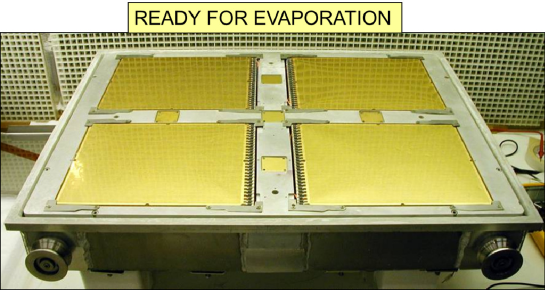
Gold GEMs are mounted four at a time into a sealed transfer box and placed into the evaporator for CsI photocathode deposition. Additionally, several small (2 cm 2 cm) Cu-Ni-Au circuit cards (called chicklets) are also mounted into the box to be used as a monitor of the quantum efficiency (QE). A set of four GEMs and five chicklets ready for evaporation is shown in Fig. 10. Once in the evaporator, the lid of the transfer box is removed to expose the GEMs. The evaporator is pumped down to a vacuum of Torr with a combination of a turbopump and a cryopump. While pumping, the transfer box containing the GEMs is heated to 40 ∘C to drive off water and other contaminants.
Facing each GEM is a molybdenum crucible with a single piece of CsI weighing 0.8 g. Once ultra high vacuum is achieved, the crucible is resistively heated to vaporize the CsI. A quartz thickness monitor positioned near the GEM surfaces is used to determine the deposition rate of the CsI. By varying the current through the crucibles, the rate is kept near 1 nm/s. The final thickness of the CsI layer is typically 300 nm.
After CsI deposition, the transfer box is moved to the QE measurement section of the evaporator. It was observed that the QE of newly deposited photocathodes can change (typically improve) by a factor of 2 over a period of 8 hours, so the measurement is not performed until this time has passed. A deuterium lamp shines through a 160 nm filter, enters the vacuum via a MgF2 window, and shines onto a movable mirror. This mirror can be rotated to allow the light to be directed either onto the GEM surface or onto a reference phototube of known QE. Once the light source has been calibrated using this phototube, the QE of the new CsI photocathode can be determined relative to the tube. A mesh with 300 V is used to draw photoelectrons from the CsI surface, which is measured as current by a picoammeter. The transfer box and phototube can both be translated inside the evaporator, allowing a scan of the entire surface of each photocathode. This measurement ensures the photo-sensitivity of each cathode across its entire surface, but only at a single wavelength. The small chicklets are later transferred to Brookhaven National Laboratory, where a scan across the wavelength range 120 nm to 200 nm is performed using a vacuum photospectrometer. It was found that every evaporation during the entire history of the project produced identical photo-sensitivity and uniformity.
3.4.4 Installation of GEM photocathodes
After the QE scan, the evaporator is backfilled with ultra high purity argon up to atmospheric pressure. The transfer box containing the gold GEMs with CsI photocathodes is then sealed in the argon atmosphere before the evaporator chamber is opened to air. The sealed transfer box is put into the glovebox through a load-lock system, which prevents any room air from entering the glovebox. The transfer box is not opened until it is inside the dry nitrogen atmosphere of the glovebox, ensuring that no humidity affects the photocathodes.
The glove box is set up in three modules, each with a distinct purpose. The first module has the rail system that accepts the transfer box from the evaporator, with a winch mounted on the ceiling to lift the transfer box lid.
The second module serves as the high voltage testing station for the gold GEMs after CsI deposition. Here the gold GEMs undergo all the above mentioned electrical tests, with the exception that the voltage in step 3 is decreased from 550 V to 500 V in the nitrogen atmosphere of the glove box. It is common for a gold GEM to exhibit several discharges upon the first application of high voltage after CsI deposition, but stabilize afterwards. Rarely a gold GEM exhibits a short or anomalous leakage current after deposition. If so, it is washed and the testing/deposition process is repeated.
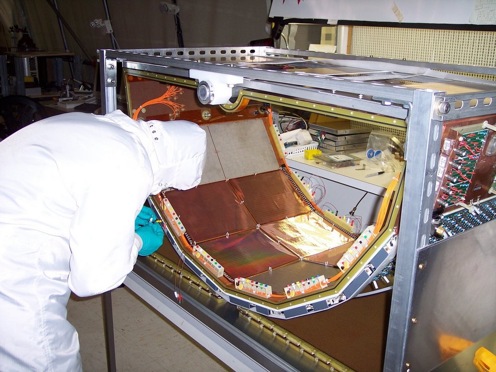
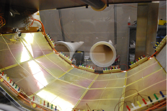
The third station houses the HBD vessel. The vessel is mounted in a rotating fixture that can be turned to allow access to the edge modules (normally out of reach of the gloves). After the gold GEMs are mounted, all three GEMs in a stack are tested in situ under high voltage. The mesh is then installed over the stack, and 500 V is applied across the drift gap to ensure that there is no electrical continuity between the GEM and mesh. A completed HBD vessel is shown in Fig. 11. The irredescent color of the GEM surfaces is created by the CsI coating.
Once all the interior components of the HBD are assembled, final tests are done to ensure that the device is fully functional. Each GEM is tested by measuring the capacitance across its HV input leads, and finally for high voltage stability. Following these tests, the sides of the vessel are installed while the vessel is still inside the glovebox, sealing the dry nitrogen atmosphere inside. The vessel is then brought out of the glovebox and onto a test bench, and purged with CF4.
3.5 Cosmic ray tests
Because many materials of the HBD (FR4, kapton) outgas water, it is necessary to store the HBD during testing with a high flow rate recirculating gas system. This system recycles CF4 gas at a rate of 2.2 slpm, and maintains water levels below 20 ppm, and oxygen below 2 ppm. Measurements of higher water contamination than oxygen are indicative of a system that is well sealed against leaks, but outgasses water from its interior surfaces.
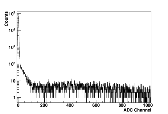
While under flow of CF4, the HBD modules are turned on one-by-one with the mesh high voltage set in the forward bias mode. This polarity of mesh voltage makes the HBD sensitive to ionizing particles and thereby cosmic ray muons. A small scintillator is placed above the sector under test and used as a trigger for pulse-height spectra taken by a CAMAC-based DAQ system. Eight hours of tests not only provide an excellent stability measurement, but also sufficient statistics from 14 pads (those shadowed by the trigger scintillator) to measure the gain of each module. A typical measurement from the cosmic ray data is shown in Fig. 12. The spectrum contains three components: (i) Pedestal (fit with a Gaussian function), (ii) Single photoelectrons from scintillation (Exponential), and (iii) Ionization from ionizing tracks (Landau). Of these three components, the response to the single photoelectrons from scintillation proved to be the most stable in establishing each module’s gain. These data were later used to set the operating voltage for each module.
3.6 Scintillaton Cubes
The photocathodes which were produced during the evaporation, installation and assembly were required to perform at maximum efficiency for the duration of the entire experiment, which spanned a period of almost two years. As described in Section 5, the HBD gas system was designed to maintain the detector gas at extremely low levels of water and oxygen, and performed extensive monitoring of these levels throughout the run. However, in order to be sure that the photocathodes did not deteriorate over time, an independent means of monitoring their quantum efficiency was developed.
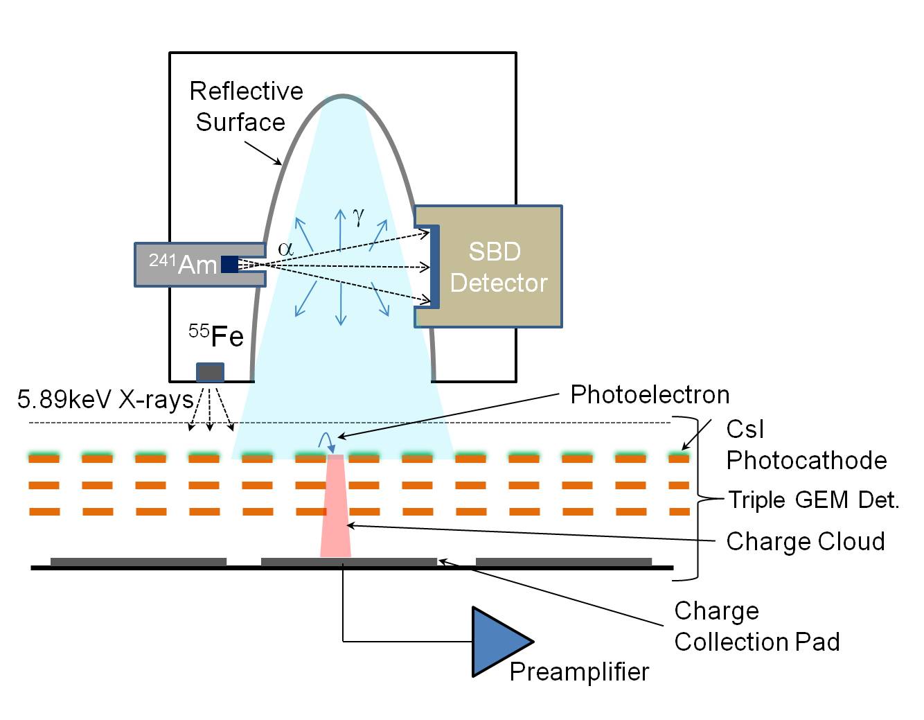
The method utilizes the scintillation light produced in CF4 to illuminate a small region of the photocathode which could be used to determine the photoelectron yield. It is then assumed that the rest of the photocathode is the same, since all photocathodes are inside the same gas volume for each half of the detector. Fig. 13 shows a schematic representation of this device. It consists of a lucite cube, which we refer to as a “scintillation cube”, in which a small (1 Ci) 241Am source is mounted. Approximately 1 cm away, a silicon surface barrier detector (SBD) is mounted to detect alpha particles which pass through the gas. The alpha particles deposit 4 MeV in the gas, and still have enough residual energy to trigger the SBD, which is used to externally trigger on the source. The scintillation light produced in the gas is focused onto the photocathode illuminating essentially one pad and producing 4-5 photoelectrons. An 55Fe source is also mounted in the cube which produces 5.9 keV X-rays that convert in the gas and allow a determination of the gas gain in the same region of the detector. Using the gas gain and the peak of the photoelectron distribution, the photoelectron yield can be determined. While this does not give us a measure of the absolute quantum efficiency, it can be used to monitor any changes in the quantum efficiency over time. Measurements of the photoelectron yield were performed several times throughout the experiment, and, as discussed in Section 7.5, no change in the quantum efficiency was observed.
4 Readout electronics
As shown in Fig. 5, the readout pads are connected by wires passing through the honeycomb back panels to individual hybrid preamplifiers located on readout boards mounted on the back of the detector. These wires were kept very short (2 cm) in order to minimize pickup and noise. The preamps plug into sockets on the readout boards, which also contain power and ground planes that form part of the overall ground plane of the detector. The entire detector is shielded by virtue of the ground planes on the readout boards and by copper cladding on all of the other FR4 structural panels. This essentially forms a complete Faraday shield for the detector, which is very important and effective in minimizing the noise on the front end readout electronics.
4.1 Hybrid preamps
The charge signal from each readout pad of the GEMs is amplified by a custom designed hybrid preamplifier (IO1195-1) developed by the Instrumentation Division at BNL. A simplified schematic circuit diagram is shown in Fig. 14. A detailed schematic can be obtained from BNL’s Instrumentation Division [14]. It uses an FET input (2SK2314) that is capable of accepting bipolar signals, but is used with only negative inputs with the HBD. The gain was set to give an output of 100 mV for an input signal of 16 fC (100,000 e), which corresponds to an average primary charge of 20 photoelectrons at a gas gain of . It has a peaking time of 70 ns and a decay time of 1 s. When connected to the GEM pad, the noise was measured to be 1000 e, which is equivalent to 0.2 photoelectrons (p.e.) at a gain of . The input to the preamp incorporates an additional FET that is used for discharge protection, which adds slightly to the noise, but helps to protect against damage from sparks. It should be noted that throughout the entire operation of the detector, not a single preamp was ever damaged due to sparking.
The output has a differential driver which has a maximum dynamic range of 1.5 V, corresponding to an input signal of up to 300 p.e., and delivers its differential output signal to a shaper located in the Front End Module (FEM). The cable used to connect the preamp to the shaper (Meritec Hard Metric 700319-01) is 10 m long and consists of 2 isolated 26 gauge parallel wires per channel with an overall shield and has an impedance of 100 . The preamp operates with 5 V and draws 165 mW per channel. The preamps were designed with a small overall profile (19 mm 15 mm) in order to minimize their mass (see Table 2).
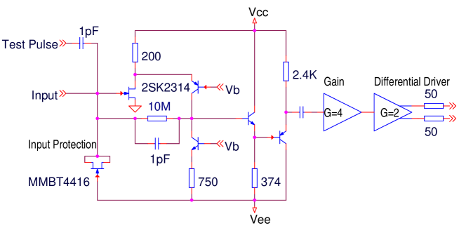
The preamp also includes a 1 pF capacitor that allows injecting a known amount of charge into the input stage. A test pulse of known amplitude is generated externally and brought in on the readout boards where it is distributed in groups of 8-12 channels to the individual preamps. The test pulse provides a convenient way to test and calibrate all the preamps on the detector and to monitor the electronic gain of the system.
4.2 Front End Module
The overall layout for the HBD FEM is shown in Fig. 15, and further details are given in [15]. The FEM receives the preamp signals using a differential receiver, which provides some additional shaping, and then digitizes them using a 65 MHz 8 channel 12 bit flash ADC (Texas Instrument ADS5272).
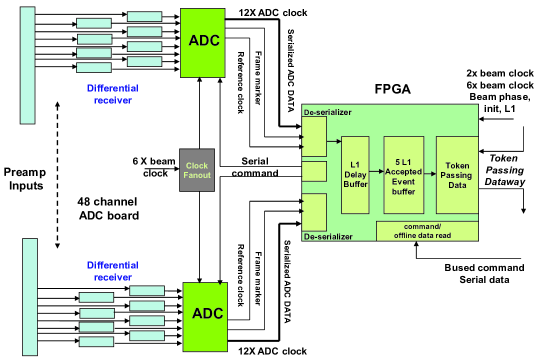
Each FEM contains six 8 channel ADCs for a total of 48 channels per module. The gain of the shaper was set such that a preamp input charge of 16 fC (105 electrons) produces a signal of 160 ADC channels (0.1 fC/ch). The preamp signal was set in the range of 1.5 V around the ADC common mode voltage, which effectively uses only half of the full dynamic range of the ADC. The ADC clock is derived from the 9.6 MHz RHIC clock at six times its frequency, i.e. 57.6 MHz, in normal data taking mode. The output of the ADC is serialized at 12 times the ADC clock and sent along with additional reference signals to an ALTERA Straitx III 60 FPGA where the data is de-serialized. The FPGA has 8 independent serializer/de-serializer blocks which are used for the eight channels of each ADC. It also provides a de-serialized function that outputs 6 bit wide data at 120 MHz, which are then regrouped into 12 bit wide ADC data within the FPGA. The PHENIX DAQ requires event buffering for up to 5 events and 40 beam crossings for its Level 1 trigger, which is also accomplished within the FPGA. The FPGA could also provide a Level 1 trigger output for the PHENIX DAQ, but this feature was never implemented during data taking.
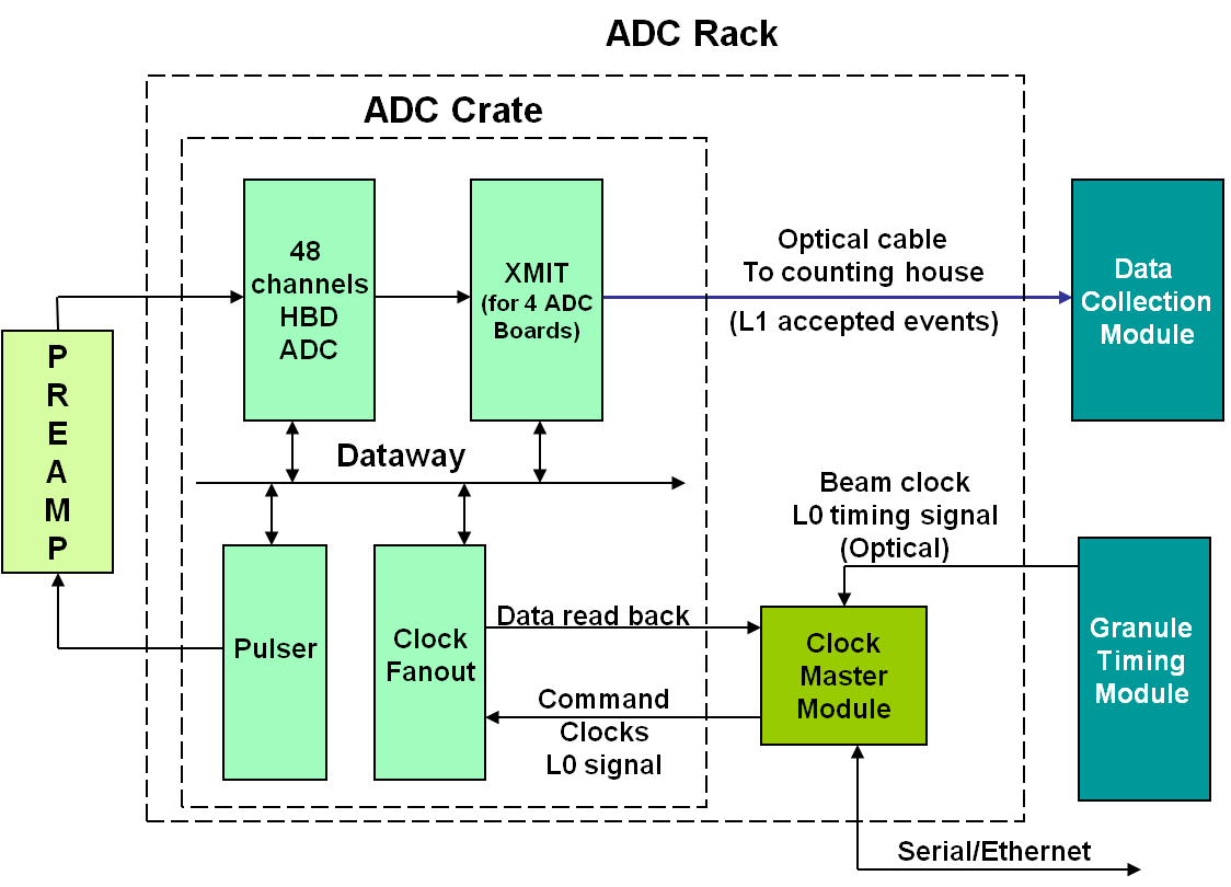
The FEM system and its interface with the overall PHENIX DAQ are shown in Fig. 16 and are further described in [15]. The FEMs are hosted in a set of 6U VME crates located in a single rack close to the detector. A custom dataway is used as a bus for serial data transmission between adjacent modules, and a Clock Master Module is used to interface with the PHENIX Granule Timing Module that provides synchronization with the PHENIX timing and control system, and also provides a separate interface for slow downloads. The Level 0 (L0) and Level 1 (L1) timing signals and serial data are generated within the Clock Master Module and sent to the FEMs. Upon receiving an L1 trigger, 12 samples of data per ADC channel are sent by optical fiber at six times the beam crossing frequency to a set of Data Collection Modules located in the PHENIX Control Room with an average transfer time of 40 s.
5 Gas system and monitoring
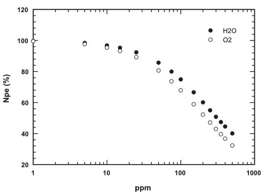
Maintaining high gas purity is a critical factor for the overall performance and operation of the HBD. In particular, impurities such as water and oxygen adversely affect the performance in several ways. Both water and oxygen have strong absorption peaks for Cherenkov light in the spectral range of sensitivity of the CsI photocathodes, and even small levels of either of these contaminants can produce a significant loss of photoelectrons. This is illustrated in Fig. 17,
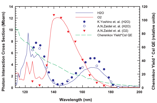
which shows the photon interaction cross sections for water and oxygen in the wavelength range of interest. Fig. 18 shows how this translates into a loss in the number of photoelectrons in a 50 cm long radiator. The main source of oxygen contamination is from leaks in the detector vessel. While these leaks are very small ( 0.12 cc/min), they nevertheless allow some diffusion of oxygen into the detector. The main source of water is from outgassing within the detector itself, particularly from the GEM foils and pad readout plane, which are made of kapton, and from the walls of the vessel, which are made of FR4. These components produce a constant source of water inside the detector which could only effectively be reduced by maintaining a high gas flow rate.
In addition, prolonged exposure to water can cause a deterioration in the CsI quantum efficiency [18], and can also affect the gain stability of the GEMs [19], although these effects were not problems at the levels at which the HBD was operated in PHENIX. Finally, CF4 is an aggressive gas requiring that all gas system components be resistant to chemical corrosion, and, in addition, CF4 is also very expensive.
These stringent demands require a sophisticated gas system that not only delivers high quality gas to the detector, but also monitors the levels of the critical contaminants to high precision. A recirculating gas system, shown in Fig. 19, is implemented in order to
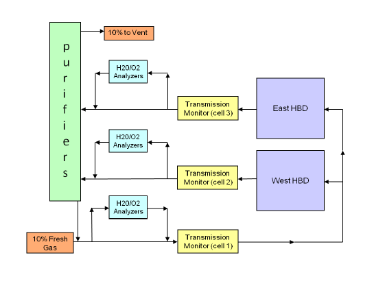
limit gas consumption and reduce operating costs [20]. The system delivers clean gas ( 1 ppm of H2O and O2) to the detector. The output gas is repurified by a set of filters and scrubbers before being reused. In addition, a percentage of fresh gas (typically 10%) is introduced during recirculation in order to help maintain the required level of purity. The main components of the system are housed in the PHENIX Gas Mixing House, which is located approximately 100 meters from the detector, and is connected to the detector though stainless steel pipes. The input gas is common to both detector arms up to a gas monitoring station located just outside the PHENIX intersection region, where it is split into separate inputs lines to the East and West detectors. Each detector has separate gas returns to the monitoring station. The flow rate was typically 3.75 l/min to each detector, and the operating pressure was 1.4 Torr above atmospheric pressure.
In order to measure and control the high gas purity required, extensive monitoring of the oxygen and water levels is implemented throughout the system. Oxygen and water sensors (GE Panamatrics O2X1 and Kahn Cermet II) are installed in the Gas Mixing House to measure the levels of the input gas at the source and the return gas before repurification. The Kahn Cermet II water sensors were chosen for their compatibility with CF4. Additional sensors are also installed for the input and return gases in the monitoring station, which measure the water and oxygen levels approximately 50 meters from the detector.
These sensors provide continuous information on the contaminant levels. However, their sensitivity at the low ppm levels achieved during normal operation is not sufficient to determine the true level of impurities in the gas. Therefore, a completely independent monitoring system was built to measure the actual UV transmission of both the input gas and the output gas of each detector.
The gas transmission monitor is shown in Fig. 20 and also further described in [20, 21]. It consists of a vacuum ultraviolet spectrometer (McPherson Model 234/302) and a set of three transmission cells that are used to measure the transmission of the common input gas and separate output gases of each detector. A scanning monochromator combined with a translatable mirror delivers a collimated beam of monochromatic light from a deuterium lamp down one of three 51 cm long transmission cells equipped with a CsI photocathode phototube (Hamamatsu R6835) on the end. One transmission cell is used for measuring the input gas and two for the output gas. A portion of the beam is also measured by a separate phototube in order to monitor the lamp intensity. The phototubes are operated in a photodiode mode and their photocathode currents are measured using two Keithley 6487 picoammeters. The monochromator, translatable mirror, and readout of the picoammeters are controlled by a Labview program running on a PC in the monitoring station.
The entire spectrometer and each transmission cell can be pumped and also purged with pure argon. After almost two years of operation of the spectrometer under vacuum, it was found that there was a significant loss in light intensity due to the buildup of deposits on the beam optics. All of the beam optics were subsequently replaced and, during the last year of operation, the main compartment of the spectrometer containing the beam optics was operated at atmospheric pressure under a flow of pure argon. However, the transmission cells were still evacuated for reference scans in order to determine the CF4 transmission relative to vacuum.
The gas transmission is defined as the double ratio of the currents, I, in the cell and in the monitor PMTs. :
The gas transmittance was measured continuously throughout each run, with scans being done sometimes several times a day to once a week or more as necessary. A typical set of input and output transmission spectra is shown in Fig. 21. Using the measured transmission values and the known absorption cross sections for water and oxygen (see Fig. 17), a fit is performed to determine the true impurity levels in the gas. The spectra are fit over a wavelength range from 111-200 nm including a component due to the intrinsic absorption in CF4 and components due to water and and oxygen impurities. This method not only allows a more precise determination of the actual impurity levels, but gives a direct indication of the total integrated absorbance in the gas.
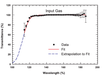
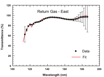
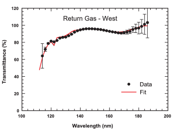
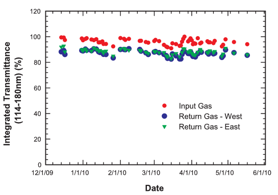
The input spectrum shows virtually no additional absorbance other than the intrinsic absorbance of the gas. The two output spectra exhibit a shape that is dominated by water absorption with a small component of oxygen (see again Fig. 17). As determined by these fits, the impurity levels of the input gas were typically less than 2 ppm of both water and oxygen, and the output gas typically showed 20-30 ppm of water and 2-3 ppm of oxygen. Fig. 22 shows the integrated transmittance over the range from 114-180 nm for a roughly five month time period during Run 10 at RHIC, and shows that the input gas was in the range from 90-100%, and the output gas was in the range from 80-90%. This was sufficient to keep the transmission loss of photoelectrons to 5% throughout the entire run.
6 High voltage system
The high voltage supply for the HBD is based on the LeCroy 1450 high voltage system, but modified with a number of additional features to improve calibration, enhance voltage and current monitoring, and provide additional trip protection capabilities. The main high voltage supply is a LeCroy 1458 mainframe equipped with a set of six LeCroy 1471N high voltage modules capable of supplying up to 200 A at 6 kV. Two channels of a 1471N unit are used for each HBD module, one to power the voltage divider for the GEMs and another to supply high voltage to the mesh. The configuration of the voltage divider and power supply to the GEM stack and the mesh is shown in Fig. 23. The 20 M resistors in series with each of the 28 segmented HV strips of the GEM are mounted on the GEM foils, while all other resistors are outside the HBD vessel. The internal resistors are used to prevent a short in one strip from affecting the high voltage to other strips in the same GEM. As described below, if a short occurs in one strip, the external divider resistor can be easily changed to compensate for the short, keeping the total effective resistance across the GEM constant.
Each of the three GEMs in a stack is powered by its own separate divider. The values for the divider resistors are chosen to provide equal voltages across each of the GEMs, relatively high fields in the two transfer gaps, and an even larger field in the induction gap, in order to improve the electron collection efficiency in the three gaps [7]. This effectively results in higher overall gain of the triple GEM stack without increasing the voltage across the GEMs. The total resistance of each leg of the divider is 84 M, giving a total resistance of 28 M for the three legs in parallel. In order to achieve a typical operating gain of 4000, the total applied voltage to the top of the divider chain is 4000 V, resulting in a total current of 143 A, and an applied voltage across each of the GEMs of 476 V, which is comfortably below the breakdown voltage for the GEMs in CF4 [7].
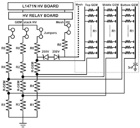
A number of additional features are built into the high voltage system to prevent excessive voltage from being applied to the GEMs or between the top GEM and the mesh. A pair of back-to-back Zener diodes installed between the mesh and the upper electrode of the top GEM limit the voltage to less than 250 V to ensure that no voltage capable of causing breakdown in this gap could be be applied. In addition, the 1471Ns HV modules were modified to incorporate a trip detection circuit that is able to recognize a trip in one channel and initiate a trip in another. This is used to trip the mesh of a given module if the GEM tripped or vice versa. The output of this circuit is connected to a custom designed “Relay Board” that utilizes high voltage relays to disconnect a tripped channel from the high voltage power supply and quickly discharge the stored energy in both the GEM stack and mesh.
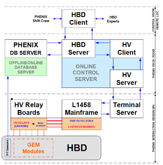
The high voltage is controlled by a High Voltage Control and Monitoring System (HVC) [22] that is designed to provide precision control of the high voltage to the detector, allowing programmable ramps, setting of standby and operational voltages for different gain settings, modification of the high voltage to compensate for pressure and temperature (P/T) changes, monitoring and recording of all voltages and currents, including storage of all values into a data base, and several modes of trip detection and recovery. The system is based on modern Optimal Control Theory and is implemented in a client-server environment using mainly Java. The overall system is shown in Fig. 24. The HBD HV Client/Server interacts through the main PHENIX HV Client/Server to communicate with the LeCroy mainframe and perform the basic HV control functions, and also provides a GUI to interact with the operators in the PHENIX Control room, or with other operators connected remotely.
In addition to the factory calibration, an in situ calibration of each 1471 module was done using the actual divider chain of each GEM. This allows precise monitoring of the current in each divider and enables detection of any additional current drawn by the GEM to a level of 100 nA, which would be an indication of a short, or partial short, in any of the GEM modules. If such an increase in current is detected, the HVC initiates a “virtual trip” and notifies the operator that intervention is required. This feature is in addition to the normal fast trip detection provided by the 1471 which causes a trip if the peak current exceeds a certain value for a short time, as in the case of a discharge. During normal operation, the fast trip thresholds are set at 20 A, and the slow or virtual trip thresholds are set to or 2 A, above the standing current value.
It should be noted that if a partial short does occur, it does not necessarily trip the power supply, but results in a small increase in current drawn by the divider chain due to the appearance of an additional resistance in parallel with the nominal 10 M resistor across each of the GEMs. However, the internal resistors in series with each of the segmented HV strips limit this parallel resistance to 20 M, even in the case of a dead short. In either case, a partial or complete short lowers the resistance, and hence the voltage across the affected GEM, thus lowering its gain. These types of shorts can be compensated for by measuring the total internal resistance of the individual GEM (20 M plus the resistance of the short) and changing the external 10 M resistor to an appropriate value to restore the total resistance to 10 M. Up to two complete shorts can be compensated for in this way without having to change any other resistors in the divider chain. In practice, during the 2010 RHIC run, only two modules showed two complete shorts and two showed partial shorts, all of which were compensated for by simply changing a single external resistor.
7 HBD operation and monitoring
A number of parameters need to be carefully adjusted and monitored to ensure good performance of the detector over a run which is typically 4-6 months long. These include setting the HV for each detector module to reach the desired operating gain, optimizing the reverse bias field in the gap between the mesh and the top GEM to achieve maximum hadron rejection while keeping maximum photoelectron collection efficiency, monitoring the gas gain variations due to pressure and temperature changes, and monitoring the gas quality and photocathode sensitivity. The monitoring of the gas quality was already discussed in Section 5. The other parameters are discussed in the present section.
7.1 Gain determination
The excellent noise performance of the readout electronics (see Section 8.1) allows the detector to be operated at a relatively low gain. During the RHIC runs of 2009 an 2010 the HBD was operated at a gain of 4,000. This gain is achieved with a voltage across the GEM 470 V, which is comfortably below the breakdown voltage of the GEMs (typically around 550 V in CF4 [7]).
The gain of each detector module is conveniently and precisely determined by exploiting the scintillation light produced by charged particles traversing the CF4 radiator. The scintillation signal is easily identified in the low amplitude part of the pulse height distribution as illustrated in Fig. 25. In the FB mode (upper panels) the spectrum has two clear components: a steep exponential distribution at very low amplitudes attributed to scintillation photons and a longer tail at higher amplitudes which is due to ionization of the gas in the drift gap. When the detector is operated in RB mode (lower panels), the latter is largely suppressed as the ionization charges get repelled to the mesh, whereas the exponential part due to scintillation remains unaffected. The scintillation signal has another characteristic feature: it produces single pad hits which are not associated to any charged track identified in the outer PHENIX detectors.
The gain G of the detector is obtained from:
| (1) |
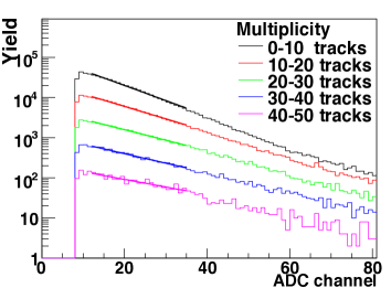
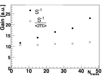
where S is the slope of the exponential shape at low amplitudes and is the average number of scintillation photons in a fired pad. In p+p collisions is very close to 1 and the gain is readily given by the inverse slope of the exponential distribution: G S-1. In Au+Au collisions however, the inverse slope increases with the number of charged particles traversing the detector as shown in the top and bottom right panels of Fig. 26. Due to the large scintillation yield of CF4, as the number of tracks increases, the probability of scintillation pile up increases and the primary charge in the scintillation signal corresponds on the average to more than one photoelectron. Assuming that the number n of scintillation photons per pad follows a Poisson distribution P(n) with an average , then is given by:
| (2) |
where P(0) is the probability to have no hit in a pad: P(0) = e-μ. Therefore:
| (3) |
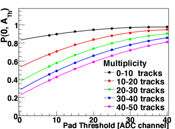
P(0) is not directly accessible since the data are always collected with an amplitude larger than some threshold value Ath and what is really measured is P(0, Ath), i.e. the probability of no hit with an amplitude larger than Ath. P(0) is determined by fitting the variation of P(0, Ath) vs Ath with some arbitrary function and extrapolating it to Ath= 0 as illustrated in the bottom left panel of Fig. 26. The gain derived using Eq. 3 is independent of the collision centrality as shown in the bottom right panel of Fig. 26.
The online gain was determined by the inverse slope of the exponent in p+p collisions. The same procedure was also used for the online determination of the gain in Au+Au collisions but selecting only very peripheral events. In both cases, the real gain calculated offline with the extrapolation procedure outlined above is only a few percent lower.
7.2 Gain equilibration
The detector gain is not uniform over its entire active area. There are two types of gain variations. There are spatial gain variations across each GEM’s area that arise from small changes in the size of the holes and from the mechanical tolerances of the various gaps. The second type of gain variations is global gain variations as a function of time which are due to changes of the atmospheric pressure and the temperature.
Gain uniformity, both in space and time, is essential for the HBD performance since its analog response is used to distinguish single from double electron hits. In order to correct for the spatial gain variations we use a gain equilibration procedure which brings all the pads in a given module to the average gain G in that module. Using a large statistics run, the average gain G is calculated from the gain Gi of each pad i determined using the procedure outlined in the previous section. The signal ai in a given pad is then corrected according to the expression:
| (4) |
An example showing the spread of gain values across the pads of one module, before and after pad gain equilibration, is shown in Fig. 27.
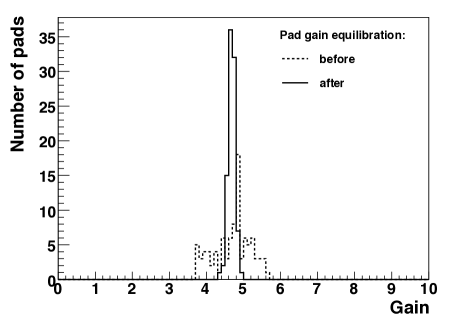
One can see that before equilibration the spread of gains is quite large with an rms of 0.45 which gets reduced to 0.10 after equilibration.
7.3 Gain variations with P/T
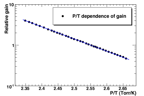
The gas gain in CF4 is very sensitive to variations of the gas density i.e. changes in P/T. The temperature of the detector is maintained fairly constant at 21oC by the temperature control in the experimental hall. However, the gas pressure varies since the detector is kept at a constant overpressure of 1.4 Torr above the atmospheric pressure and the atmospheric pressure varies greatly according to weather conditions. The detector is quite sensitive to these changes as can be seen in Fig. 28. A change of P/T by 6% induces a factor of 2 change in the gas gain. The solid line represents a fit of the data with an exponential function demonstrating that the gain varies exponentially with P/T.
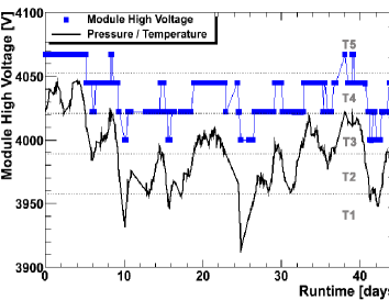
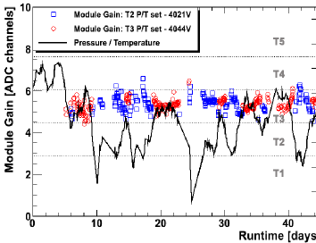
To avoid these large excursions of the gain, we defined 5 pre-determined P/T windows such that over each of them the gain varies by not more than 20%. We compensated the gain variations by automatically varying the operating HV whenever the P/T values crossed the window boundaries. The left panel of Fig. 29 shows the applied voltage to a given detector module and the P/T values over an extended period of 45 days during Run-10. The measured gain of the same module during the same time period is shown in the right panel, demonstrating that the gain is kept constant within 10%.
7.4 Reverse bias
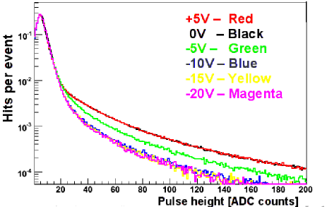
Optimizing the reverse bias mode of operation is of prime importance for the performance of the detector. As shown in [8], the ionization signal in the gap between the mesh and the top GEM drops sharply as the field is reversed and the primary charges get repelled towards the mesh. The signal drops quickly by almost a factor of 10 within 10 V, while the photoelectron collection efficiency drops much more slowly. Achieving maximum hadron rejection while keeping maximum photoelectron collection requires setting the relative voltage between the mesh and the top GEM very close to 0 with a precision of a few volts out of 4000 V applied to the voltage divider, which is far beyond the precision of the absolute high voltage values of the LeCroy 1471N power supplies. An accurate and fast method to adjust the mesh HV with respect to the GEM divider voltage was developed that exploits the scintillation signal. For each module, a series of short measurements were done where the gain was kept constant and the voltage across the gap between the mesh and the top GEM was varied in steps of 5 V. An example of such a voltage scan is shown in Fig. 30 for one particular module. For a meaningful comparison among the different spectra, the ordinate is normalized to represent the number of hits per event. One sees that the yield of the scintillation signal remains unaffected when the voltage of the mesh varies from +5 to -20 V with respect to the top GEM, whereas the ionization signal sharply drops within this voltage scan. For this module the optimal mesh voltage is -10 V with respect to the top GEM, i.e. the minimal voltage needed that produces the maximal reduction of the ionization tail.
7.5 Monitoring photocathode sensitivity
Maintaining high quantum efficiency of the CsI photocathodes was crucial for achieving maximum photoelecton yield and it was therefore important to monitor their stability and performance throughout the run. Monitoring was accomplished using two scintillation cubes mounted inside the two halves of the detector described in Section 3.6. Alpha particles from the 241Am source mounted inside the cube produce scintillation light which is focused on the CsI photocathode in one location inside each detector. The amount of light is sufficient to produce 4-5 photoelectrons, which have a Poisson distribution that can be used to determine the photoelectron
yield. In addition, the 55Fe source mounted in the cube in approximately the same location provides a means to determine the gas gain, which allows a determination of the peak of the Poisson distribution in terms of photoelectrons. The number of photoelectrons determined using the gas gain can also be compared to the number given by the shape of the Poisson distribution convoluted with the fluctuations due to gas gain and electronic noise. The two methods generally agreed quite well.
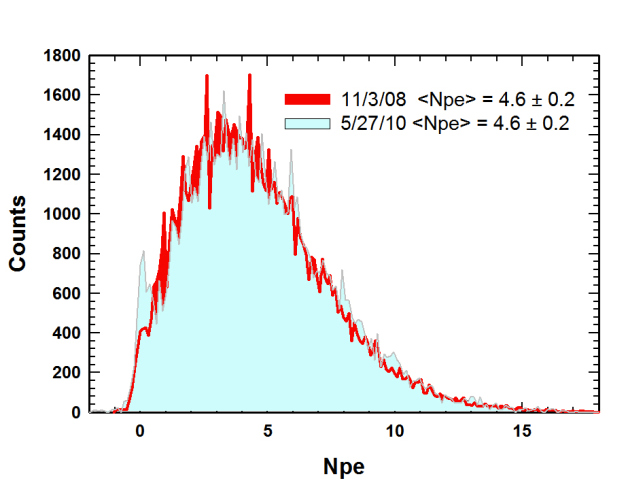
Measuring the photoelectron yield from the cube requires setting up a special readout configuration that is rather disruptive to the normal operating mode of the detector, and consequently, the measurements of the photoelectron yield from the cubes were not done very frequently (typically only once or twice per run). However, each time the measurements were done, we observed no change in the photoelectron yield, and hence the quantum efficiency of the photocathodes, from when the photocathodes were originally produced. Fig. 31 shows the photoelectron distribution measured with the scintillation cube in the West detector in November of 2008 and in May of 2010, demonstrating that the photoelectron yield of 4.6 0.2 did not change over this period of more than 18 months.
8 Performance
8.1 Noise
The signals from the GEM readout system are amplified by pre-amplifiers installed outside of the HBD detector, and sent to the front end module (FEM), 5 m away from the detector, as described in Section 4. Fig. 32 shows the mean value and width () of the
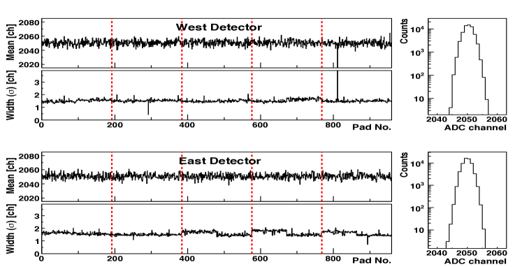
pedestal distributions for all pads in the West and East detectors. The pedestal mean values sit close to the middle of the dynamic range (4096 ADC counts). As shown in the figure, the noise level is almost the same in all pads with a typical sigma value of 1.5 ADC channels. The histograms on the right of Fig. 32 show the pedestal distributions for one single pad demonstrating a Gaussian distribution over more than three orders of magnitude. To reduce the data volume, an online zero-suppression was applied requiring the pad signal to be larger than 5 ADC channels i.e. larger than the pedestal mean.
The left panel of Fig. 33 shows a typical FADC histogram for an electron signal in the detector.
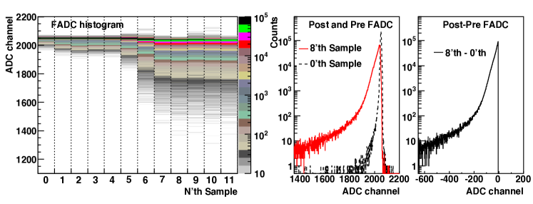
Twelve samples are taken at a rate of 57.6 MHz, corresponding to 17.4 ns time bins, and spanning an interval of 209 ns. In the offline analysis, the signal is defined as the difference of the samples (8+9+10) - (0+1+2). The zero-suppression is applied to the difference of sample 0 and 8. In the right plot, the difference of sample 8 and 0 is shown. The width of the distribution is narrower than the sample 8 itself. This is because the low frequency component of the noise is eliminated by subtracting the 0th sample. This subtraction also makes it possible to calculate the net charge when signal pile-up occurs.
8.2 Pattern recognition
The pad size (hexagon shape with side a = 15.5 mm and area = 6.2 cm2) was chosen to be comparable but smaller than the blob size (area = 9.9 cm2) such that an incident electron produces a signal distributed over a small cluster of a few pads. For single electrons the cluster size is typically 2-3 pads whereas a somewhat larger cluster is produced by close pairs from conversions or Dalitz decays. On the other hand a hadron typically produces a single pad hit.
A simple cluster finding algorithm is used to identify electron candidates in the detector. Clusters are built around a seed pad having a charge larger than a selected threshold (typically 3-5 photoelectrons). In a first step, the fired pads among the first six neighbors of the seed are added to the seed. A pad is considered fired if it has a signal larger than typically one photoelectron. In a second step clusters that have in common at least one fired pad are merged together to form a single larger cluster. The total charge of the cluster is determined as the sum of charges of the pads assigned to the cluster. The center of gravity of the cluster is taken as the hit position of the incident particle.
8.3 Position resolution
The HBD position resolution is determined from the matching of tracks defined in the PHENIX central arm detectors to HBD clusters. Fig. 34 shows the matching distribution i.e. the distance between the track projection point onto the HBD photocathode plane and the closest HBD cluster, in the (left panel) and Z (right panel) directions. These distributions were obtained from the p+p run of 2009 using a highly pure sample of electron pairs originating from Dalitz decays (with a mass = 50-150 MeV/c2) fully reconstructed in the PHENIX central arms. The matching distributions have almost no background of random matching as expected from a highly pure sample of electrons and from a very efficient detector. The electron detection efficiency will be discussed in Section 8.7.
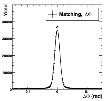
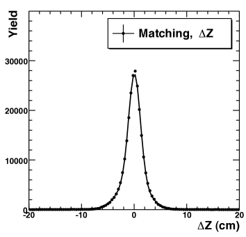
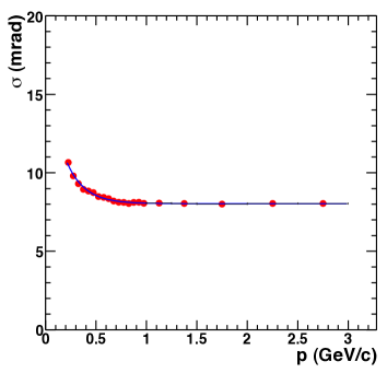
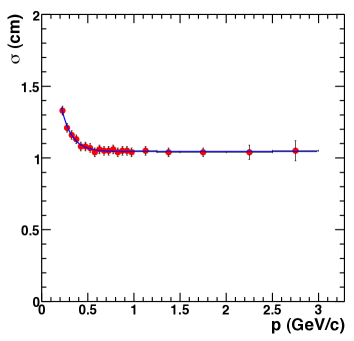
The distributions exhibit a Gaussian shape as demonstrated by the fits in the figure. They are used to align the HBD with respect to the central arm detectors by requiring the centroid of the distributions to be centered at 0. The values of the fits are presented as function of the track momentum in Fig. 35. They show the expected 1/p dependence at low momenta and a constant value at high momenta representing the intrinsic detector resolution. The latter is dominated by the size of the hexagonal pads. The position resolution of single pad hits is expected to be given by 2a/= 0.9 cm. For electron tracks, the center of gravity hit determination leads to a better resolution resulting in the asymptotic value of 8 mrad or 4.8 mm. This value is taken as the HBD intrinsic position resolution since the central arm track is determined with much better precision. In the Z direction the asymptotic resolution of 1.05 cm results from the quadratic sum of the intrinsic detector resolution and the Z resolution of the vertex position which is about 1 cm in p+p collisions.
8.4 Hadron response and hadron rejection factor
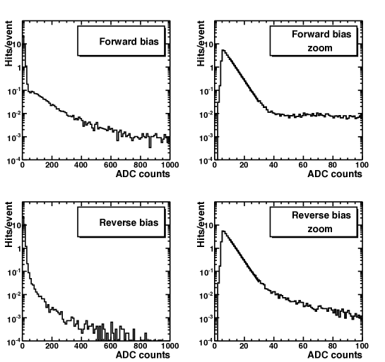
The left panel of Fig. 36 shows the HBD response to hadrons in the FB and RB modes. Hadrons identified in the central arm detectors are projected into the HBD and the amplitude of the closest cluster within matching windows in and Z is plotted. The signal is expressed in terms of the primary ionization charge, using the measured detector gain. The FB spectrum is well reproduced by a Landau distribution characteristic of the energy loss of minimum ionizing particles. The measured mean amplitude is consistent with an energy loss of dE/dx = 7 keV/cm [23] and a primary ionization of 50 eV/ ion-pair.
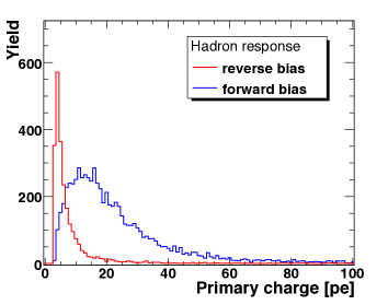
In RB, there is a sharp drop in the pulse height as the primary charges get repelled towards the mesh. In this mode, the pulse height distribution results from the collection of (i) ionization charges from a thin layer of about 100 m above the first GEM surface and (ii) ionization charges from the entire first transfer gap, which are subject to a two-stage amplification [8].
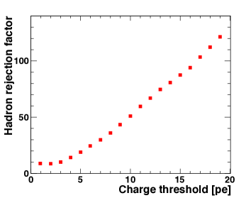
We define the hadron rejection factor as the ratio of the number of hadron tracks identified in the central arm detectors to the number of corresponding matched hits in the HBD with a signal larger than a pre-determined charge threshold. The hadron rejection factor derived from the hadron spectra measured in RB is shown in the right panel of Fig. 36 as function of the charge threshold. The rejection is limited by the long Landau tail and depends on the charge threshold that can be applied without compromising too much the single electron detection efficiency. Rejection factors of the order of 50 can be achieved with an amplitude threshold of 10 e.
8.5 Single versus double electron response
As mentioned in the Introduction, the combinatorial background originates mainly from Dalitz decays and conversions. Most of these pairs are reconstructed in the HBD as a double electron cluster (overlapping electron and positron hits) due to their small opening angle and the coarse granularity of the HBD pad readout. The HBD exploits these two facts and reduces the combinatorial background by rejecting central arm electron tracks if the associated hit in the HBD has a double hit response or if there is a nearby hit within an opening angle of typically 200 mrad. This is done by two cuts, an analog cut and a close hit cut, respectively. The analog cut requires good separation between single and double electron hits, whereas the close hit cut requires good hadron rejection in order not to veto the signal with the overwhelming yield of hadrons.
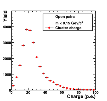
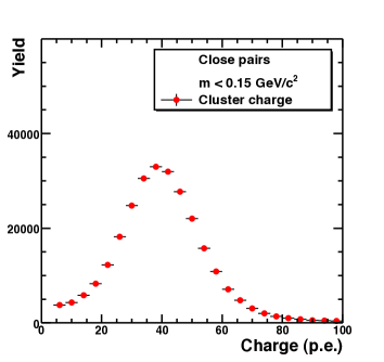
In order to study the HBD response to single and double electrons, we select a sample of pairs in the mass region below 0.15 GeV/c2 where the combinatorial background is negligible. This sample is divided into two categories: if both the electron and positron tracks reconstructed in the PHENIX central arms are matched within 3 in both and Z directions to two separate HBD clusters we interpret this as the response of the HBD to single electrons. If they are matched to the same HBD cluster we interpret it as the HBD response to a double electron. The HBD single electron response is shown in the left panel of Fig. 37, whereas the HBD double electron response is shown in the right panel. The former is peaked at around 20 photoelectrons, whereas the latter is peaked at about twice that value, at 40 photoelectrons. The mean value of the tagged single electrons is significantly higher, probably reflecting the fact that this sample contains a small fraction of double electron hits. We therefore take the peak values of 20 and 40 photoelectrons to represent the mean HBD response to single and double electrons respectively.
8.6 Figure of merit N0 and photon yield
The average number of photoelectrons Npe in a Cherenkov counter with a radiator of length L is given by:
| (5) |
where is the average Cherenkov threshold over the sensitive bandwidth of the detector and N0 is the figure of merit of the Cherenkov counter.
The ideal figure of merit, i.e. in the absence of any losses, is obtained by integrating the CsI quantum efficiency (QE) times the CF4 gas transmission (TG) over the sensitive bandwidth of the detector. The HBD is sensitive to photons between the ionization threshold of the CsI photocathode (6.2 eV) and the CF4 cut-off (the 50% cut-off point is at 11.1 eV and the transmission drops to zero at 12.4 eV). For the CsI QE in CF4 we use our measured values given in [8] where it was shown that the QE increases linearly from 6.2 eV to 10.2 eV (corresponding to the highest energy where it was measured). We assume the same linear dependence to extrapolate the QE from 10.2 eV till the absolute cut-off at 12.4 eV. For TG we use our measured values (see below). We then obtain an ideal value for N0 of:
| (6) |
In the actual detector, this figure gets degraded by a number of factors that reduce the overall photoelectron yield. These include the transparency of the radiator gas, TG, the optical transparency of the entrance mesh, TM, the optical transparency of the top GEM (which reduces the effective photocathode area), TPC, the loss of photoelectrons due to the reverse bias mode of operation, , the transport efficiency of the photoelectrons, once extracted from the photocathode, into the holes of the GEM, , and the loss of signal due to the pad amplitude threshold that is applied to the readout, . Some of these efficiencies are wavelength independent and straightforward to measure or estimate, while others are wavelength dependent and may have greater uncertainties. In the following we discuss all these factors and quote their average values in Table 3.
The optical transparency of the mesh, TM, is simply determined by the opacity of the wire mesh and was calculated to be 88.5%.
The optical transparency of the photocathode, TPC, gives the effective area of the photocathode and is determined by the hole pattern in the GEM foil. However, the GEM holes are not perfectly cylindrical and have a tapered shape that consists of an outer hole in the copper layer and an inner hole in the kapton. By measuring the photocathode efficiency of a solid planar photocathode and comparing it with that of a photocathode deposited on a GEM foil, we determined that the effective photocathode area of the GEM is given by the average of the inner and outer hole diameters. This leads to an average value for the optical transparency of the GEM foil of 81% as given in Table 3.
The radiator gas transparency TG consists of the intrinsic transmission of CF4 combined with the absorption caused by any impurities such as oxygen and water. The intrinsic transmission of the HBD gas is essentially given by the transmission of input gas as shown in the top panel of Fig. 21, and the transmission including the oxygen and water impurities in the output gas is shown in the lower panels of Fig. 21. The shape of the transmission spectrum at the shortest wavelengths is not measured with high precision due to limitations in the light output of the transmission monitor. In order to obtain the transmission down to the UV cutoff, it is assumed that the shape of the spectrum is a symmetric S-shaped curve with a 50% transmission point at 111 nm, which is then extrapolated down to an absolute cut-off of 100 nm. We estimate that this approximation leads to an uncertainty of 10 % in our estimation of the photoelectron yield. Using typical transmission curves with 20 ppm of water and 3 ppm of oxygen, we obtain an average value of 89% for the gas transmission as given in Table 3.
The transport efficiency, , for transferring photoelectrons produced on the photocathode to the holes in the GEMs was measured in [24]. The value is independent of wavelength and is given as 80% in Table 3.
Finally, the losses due to reverse bias operation, , as described in [8], were minimized by optimizing the reverse bias operating point for each module, as described in Section 7.4. These losses, along with the loss of signal due to the amplitude threshold applied in the readout, , is estimated to be 90% as given in Table 3.
With all of these losses, the expected figure of merit is computed to be N = 328 cm-1 with an estimated uncertainty of 14%. The uncertainty comes primarily from the CF4 transmission near its cut-off, and from the extrapolation of the CsI QE from from 10.2 eV to the CF4 cut-off. Using the calculated average = 28.8 [25] and an average radiator length of L = 51.5 cm, the expected number of photoelectrons is 20.42.9. A more accurate calculation based on the convolution of the QE with the gas transmission and (which varies with wavelength due to the chromatic aberration) according to:
| (7) |
gives a very similar value of Npe = 20.32.8.
| N0 ideal value | 714 cm-1 |
|---|---|
| Optical transparency of mesh | 88.5% |
| Optical transparency of photocathode | 81% |
| Radiator gas transparency | 89% |
| Transport efficiency | 80% |
| Reverse bias and pad threshold | 90% |
| N0 calculated value | 328 46 cm-1 |
| Npe expected | 20.4 2.9 |
| Npe measured | 20 |
| N0 measured value | 322 cm-1 |
The experimental number was obtained from a sample of resolved Dalitz pairs as defined in Section 8.5, i.e. pairs reconstructed in the central arms with a mass 150 MeV/c2 matched to resolved clusters in the HBD. As shown in Fig. 37, the HBD response to these single electrons gives a most probable value of N 20 photoelectrons corresponding to a measured figure of merit N = 322 cm-1, in very good agreement with the calculated values. The observed N0 value is very large compared to those achieved in any other gas Cherenkov counter [26, 27, 28, 29].
8.7 Single electron efficiency
The HBD single electron identification efficiency is a key factor for the dilepton physics with the HBD. The electrons reconstructed in the PHENIX central arms cannot be used to determine the HBD single electron efficiency since most of them do not originate from the vertex but from downstream conversions. We have used two methods to determine the HBD electron efficiency. In the first method, we select a sample of reconstructed Dalitz open pairs with low mass where the number of the conversions is relatively small and where the combinatorial background is negligible, namely 25 50 MeV/c2. The conversions in this mass window are effectively removed by applying a cut on the orientation of the pairs in the magnetic field [5]. The electrons in this sample are matched to hits in the HBD within a 3 matching window and the ratio of the matched hits to the total number of electrons define the HBD single electron efficiency. This ratio is plotted in Fig. 38 as function of the cut. The figure demonstrates that the efficiency averaged over the entire detector is close to . Most of the losses occur near the edges of the detector modules. Excluding the boundaries results in an efficiency close to 100 %.
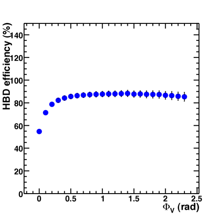
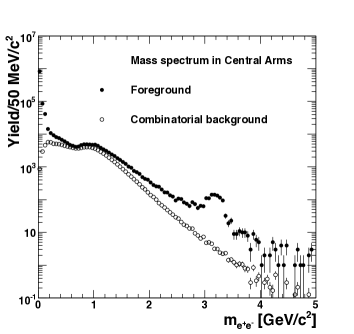
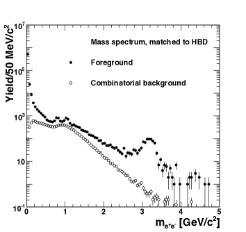
In the second method, we use the sample of fully reconstructed pairs in the high mass region ( 2.5 GeV/c2) from the p+p run of 2009. This sample is dominated by decay into pairs with a relatively low background, consisting of combinatorial pairs and correlated pairs from the semileptonic decays of charmed mesons. The left panel of Fig. 39 shows the invariant mass spectrum measured (solid dots) in = 200 GeV p+p collisions using the PHENIX central arms only. The combinatorial background evaluated by a mixed event technique is shown by the open circles. The right panel shows the same mass spectrum after requiring a matching of the electron and positron tracks to hits in the HBD. The matching to the HBD effectively removes conversions occurring downstream of the HBD and misidentified electrons in the central arms and consequently the combinatorial background is considerably reduced as demonstrated in the right panel. On the other hand, the yield is almost preserved. A proper evaluation of the yield can be obtained by fitting the mass spectrum (after subtraction of the combinatorial background) in the vicinity of the peak with a Gaussian function (for the ) plus an exponential function for the open charm contribution. Comparing the so extracted yield before and after matching to the HBD, gives also a single electron efficiency of for the entire HBD detector.
9 Summary
We described the concept, construction, operation and performance of the Hadron Blind Detector that was developed for the PHENIX experiment at RHIC. The HBD is a Cherenkov detector with a 50 cm long CF4 radiator connected in a windowless configuration to a triple GEM coupled to a pad readout and with a CsI photocathode layer evaporated on the top face of the GEM stack. The detector was successfully operated in the 2009 and 2010 RHIC runs where large samples of p+p and Au+Au collisions, respectively, were recorded. The detector showed very good performance in terms of noise, stability, position resolution, hadron rejection, single vs. double hit recognition and single electron detection efficiency. The novel concept of using CF4 in a windowless configuration results in an unprecedented bandwidth of sensitivity from 6.2 eV (the threshold of the CsI photocathode) up to 11.1 eV (the CF4 cut-off). This translated in a measured figure of merit N0 of 330 cm-1, much higher that in any other existing gas Cherenkov detector.
10 Acknowledgements
We are grateful to the PHENIX Collaboration for their support and help during the various phases of the HBD upgrade project. We are grateful to Franco Garibaldi and his group from INFN, Roma for loaning to us their CsI evaporation facility. We are grateful for the technical support of Mr. Richard Hutter, Mr. Richard Lefferts and Mrs. Lilia Goffer. We acknowledge support of the work at Brookhaven National Lab by the U.S. Department of Energy, Division of Nuclear Physics, under Prime Contract No. DE-AC02-98CH10886, at Columbia University’s Nevis Labs by the U.S. Department of Energy, Division of Nuclear Physics, under Prime Contract No. DE-FG02-86ER40281, at Stony Brook University by the U.S. National Science Foundation under contract PHY-0521536 and by the U.S. Departement of Energy, Division of Nuclear Physics under contract DEFG - 0296ER40980, and at the Weizmann Institute of Science by the Israeli Science Foundation, the Minerva Foundation with funding from the Federal German Ministry for Education and Research and the Leon and Nella Benoziyo Center for High Energy Physics.
References
- [1] K. Adcox et al., Nucl. Phys. A757 (2005) 184.
- [2] see e.g. review articles in Landolt-Boernstein New Series Vol I-23, (2010), arXiv:0903.0415 and arXiv:0901.3289.
- [3] A. Adare et al., Phys. Rev. Lett. 104 (2010) 132301.
- [4] K. Adcox et al., Nucl. Instr. and Meth. A499 (2003) 469.
- [5] A. Adare et al., Phys. Rev. C81 (2010) 034911.
- [6] F. Sauli, Nucl. Instr. and Meth. A386 (1997) 531.
- [7] A. Kozlov et al, Nucl. Instr. and Meth. A523 (2004) 345.
- [8] Z. Fraenkel et al., Nucl. Instr. and Meth. A546 (2005) 466.
- [9] I. Tserruya, Nucl. Instr. and Meth. A563 (2006) 333.
- [10] C. Woody et al., Proc. of the 2006 IEEE NSS/MIC Conference, San Diego, CA, Oct. 16-23, 2006 and Proc. of the 2009 IEEE NSS/MIC Conference, Orlando, FL, Oct. 25-31, 2009.
- [11] J. Almeida et al., Nucl. Instr. and Meth. A361 (1995) 524.
- [12] F. Cusanno et al., Nucl. Instr. and Meth. A502 (2003) 251.
- [13] F. Cusanno, F. Garibaldi, E. Cisbani, S. Colilli, G. De Cataldo, R. De Leo, F. Giuliani, M. Gricia, L. Lagamba, M. Lucentini, B. Reitz, F. Santavenere, G. M. Urciuoli, Nucl. Instr. and Meth. A525 (2004) 163.
- [14] BNL Instrumentation Division, http://www.inst.bnl.gov/
- [15] C-Y. Chi et.al, Proc. of the 2007 IEEE NSS/MIC Conference, Honolulu, Oct. 25 - Nov. 1, 2007.
- [16] A. N. Zaidel and E.Ya. Sheider, Vacuum Ultraviolet Spectroscopy, Ann Arbor-Humphrey Science Publishers, 1970.
- [17] K. Yoshino, J.R. Esmond, W.H. Parkinson, K. Ito and T. Matsui, J. Chem. Phys. 211 (1996) 387.
- [18] A. Breskin et.al., Nucl. Instr. and Meth. A471, 333 (2000).
- [19] B. Azmoun et al., Proc. of the 2006 IEEE NSS/MIC Conference, San Diego, CA, Oct. 16-23, 2006.
- [20] S. Stoll et al., Proc. of the 2007 IEEE NSS/MIC Conference, Honolulu, Oct. 24 - Nov. 1, 2007.
- [21] B. Azmoun et al., Proc. of the 2010 IEEE NSS/MIC Conference, Knoxville, TN, Oct. 30 - Nov. 5, 2010.
- [22] M. Proissl, Masters of Science thesis, Physics Department, Stony Brook University, December 2009.
- [23] D. S. Denisov, Nucl. Instr. and Meth. A306 (1991) 200.
- [24] B. Azmoun et al., IEEE Trans. Nucl. Sci. 56-3 (2009) 1544.
- [25] R. Abjean, A. Bideau-Mehu, Y. Guern, Nucl. Instr. and Meth. A292 (1990) 593.
- [26] R. Baur et al., Nucl. Instr. and Meth. A343(1994) 87.
- [27] J. Seguinot and T. Ypsilantis, Nucl. Instr. and Meth. A433 (1999) 1.
- [28] Y. Akiba et al., Nucl. Instr. and Meth. A433 (1999) 143.
- [29] E. Nappi and J. Seguinot, Nuovo Cimento 28 (2005) 1.