Klein Tunneling and Berry Phase in Bilayer Graphene with a Band Gap
Abstract
Klein tunneling in gapless bilayer graphene, perfect reflection of electrons injecting normal to a junction, is expected to disappear in the presence of energy band gap induced by external gates. We theoretically show that the Klein effect still exists in gapped bilayer graphene, provided that the gaps in the and regions are balanced such that the polarization of electron pseudospin has the same normal component to the bilayer plane in the regions. We attribute the Klein effect to Berry phase (rather than the conventional value of bilayer graphene) and to electron-hole and time-reversal symmetries. The Klein effect and the Berry phase can be identified in an electronic Veselago lens, an important component of graphene-based electron optics.
pacs:
72.80.Vp, 73.23.Ad, 03.65.Vf, 73.40.LqIntroduction.— Klein tunneling in graphene is a striking phenomenon Katsnelson , analogous to the behavior of relativistic particles. In monolayer graphene, it predicts that a low-energy electron (massless Dirac fermion) injecting normal to a potential step perfectly transmits through the step regardless of the step height. This effect results from the chirality of the electron Katsnelson ; NetoRMP ; Beenakker ; Cheianov , i.e., the backscattering is forbidden by the orthogonality of the pseudospins of two electrons moving in the opposite direction. It is also attributed to Berry phase Ando ; Novoselov1 ; Zhang1 of the pseudospin, as it is accompanied by a jump in reflection phase by around the normal injection Shytov . Experimental efforts have been done to observe the perfect transmission Gordon ; Gorbachev and the phase jump Young .
On the other hand, Bernal-stacked bilayer graphene has different features from the monolayer. Its low-energy electrons are massive Dirac fermions having pseudospin of different origin from the monolayer, showing Klein tunneling of the opposite behavior, perfect reflection of electrons injecting normal to a junction Katsnelson . However, little attention has been paid to the bilayer Klein effect, although it may play a crucial role in bilayer graphene electronics, which has attracted much attention because of the tunability of energy band gap McCann ; Ohta ; Castro ; Oostinga ; Zhang2 ; Nandkishore . For instance, it has not been reported whether the effect survives in the presence of a band gap, which is difficult to avoid in the junction formed by external gates. It is also meaningful to see the fundamental link of the effect with Berry phase of the bilayer Novoselov2 , and with electron focusing in Veselago lens Veselago ; CheianovLens for electron optics.

In this Letter, we study the Klein effect in Bernal-stacked bilayer graphene bipolar ( or ) junction with band gap. The Klein effect is found to survive in the presence of the gap, provided that the gaps in the and regions are balanced such that electrons have the same value of in the regions, where is the component of pseudospin polarization vector [see Eq. (3)] normal to the bilayer plane. We attribute the effect to Berry phase and to the electron-hole and time-reversal symmetries defined in a single valley of graphene. The Berry phase results in the jump by of the transmission phase through a (or ) interface around the normal incidence of electrons to the interface. On the other hand, the Klein effect disappears, i.e., the transmission of electrons with normal incidence is finite, when differs between the and regions. We show how to detect this effect and the Berry phase in a Veselago lens.
Setup.— The junction in Fig. 1 is formed by position-dependent potential energy and a band gap,
| (1) |
Assuming that and smoothly vary in the length scale of lattice constant, we ignore the mixing between K and K′ valleys of the graphene. An electron state with low energy in the K valley is governed by the massive Dirac Hamiltonian McCann of the junction,
| (2) |
and the K′ valley is described by a similar Hamiltonian. has the pseudospin components describing the lattice sites A1 and B2 of the bilayer, where Al and Bl denote the two basis sites of layer . is the pseudospin Pauli operator, is the momentum measured relative to the valley center, is the interlayer (B1-A2) coupling, and m/s. We assume the low-energy regime of , ignore the trigonal warping McCann by assuming , and also ignore the case of [i.e., in Eq. (3)] in which electron states with are evanescent waves inside the band gaps. Without loss of generality, we set hereafter; see Fig. 1(b).
We calculate the transmission coefficient and probability of an electron with through the junction, as a function of its incidence angle to the interface at ; at the normal incidence. We below consider electrons in the K valley only, as the K′ valley shows the same result; while is valley dependent at finite in a junction Schomerus , it is independent in the junction in Fig. 1 because of its left-right symmetry with respect to . The electron has the wave function of due to the translation invariance along , where is the wave vector along and is written as a superposition of propagating and evanescent waves. The continuity of and at under Eq. (2) determines Katsnelson .
For further discussion, it is useful to see the pseudospin polarization vector of the electron, where is the wave function in the region of . While is parallel to the bilayer () plane (i.e., ) in the case of zero band gap, one can show from Eq. (2) that for finite gap it has a finite value of as
| (3) |
where propagation angle in region .
As shown in Fig. 2(a), we find that the Klein effect survives ( at , irrespective of and ) even in the case of finite gap, provided (i.e., ) and electron wavelength ; the condition of suppresses electron tunneling through the central region with width , and in the region. Notice that the condition of includes the zero-gap case of . The Klein effect also occurs in a () interface, provided .
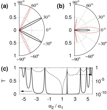
The Klein effect in the zero-gap case of Katsnelson can be understood from the fact that for electrons with normal incidence of , the pseudospin polarization vectors of the and regions are orthogonal to each other, resulting in the perfect reflection of . In the case of finite gap with , however, naive application of this argument cannot explain the Klein effect, as is not orthogonal to as shown in Fig. 1(b). We find that when , there exists a unitary operator rotating electron pseudospinor such that the resulting polarization vectors ’s in the and regions are orthogonal to each other; see Fig. 1(c). Mathematically, after the pseudospinor rotation by , the continuity equations of and at become identical to those of the zero-gap case of , which guarantees the Klein effect in the case. Physically, the rotation by allows us to explain the Klein effect by Berry phase at the interface of (or at ), as below.
To see the connection to the Berry phase, we rotate the Hamiltonian by at in the case,
| (4) | |||
We here write the expression of , , where , , is the identity, and for the electron (hole)-like band. The term in causes the chiral property that the pseudospin of is parallel to in both electron-like and hole-like bands; this property of the same chirality between electron and hole bands is introduced by the sign factor in our definition of . Because of the chirality, the pseudospin rotates following the rotation of during the scattering process at the interfaces of , and the vectors constitute the parameter space for the Berry phase associated to the pseudospin of the electron propagating with real . Note that has the same form as the Hamiltonian of the zero-gap case, and that should not be interpreted as a Hamiltonian, since the rotation is performed at the given energy .
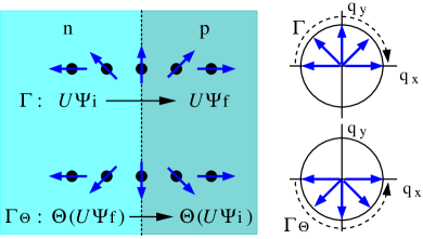
Another important feature of the case is the symmetry of described by the antiunitary operator ,
| (5) |
Here, is the electron-hole conversion operator Beenakker , is the effective time-reversal operator Beenakker , transforming to and defined in a single valley, and is the complex conjugation operator. It is a good symmetry, , and plays an important role as below. Note that has not been discussed in literature.
Now, combining the chirality and the symmetry in , we are able to connect the Klein effect with Berry phase ; see Fig. 3. We consider an incident (electron-like) state of which injects normal to the interface with at , and its transmitted (hole-like) state . The evolution from to is denoted by . The vector of the state rotates by angle (clockwise or counterclockwise) due to the electron-hole conversion during the evolution, and the pseudospin of the state rotates following the rotation of due to the chirality. On the other hand, the symmetry guarantees that there is another degenerate state injecting normal to the interface, and that it evolves from to along the reversal process denoted by , in which the rotation of and pseudospin is opposite to that of . The evolution of pseudospin along differs from that along by rotation, i.e., the difference forms a loop encircling once the origin of the space, which causes Berry phase . The Berry phase makes the destructive interference between and , hence resulting in the perfect reflection of at the interface, the bilayer Klein effect. Here, is the transmission coefficient through the interface.
In addition to the perfect reflection, the Berry phase also induces the phase jump of by around normal incidence of . We derive around ,
| (6) |
Here, and . This result is understood by considering a state injecting to the interface with incidence angle of , . The evolution of this state approximately follows . There is another state with following . As varies from to , the evolution changes from to , hence the phase of jumps by the Berry phase at .
Next, we discuss the case. In this case, the symmetry argument in Fig. 3 is not applicable, and is nonzero at ; see Fig. 2(b) and (c). To see more details, we derive at in an junction with ,
| (7) |
Here , , and . The first term of shows the suppression of the Klein effect in the case of . It oscillates with . The second term comes from the tunneling via the evanescent waves in the central region.
We compare the bipolar junction with a bilayer monopolar ( or ) junction. The monopolar case has different symmetry from Park . So, electrons injecting normal to the monopolar junction is not perfectly reflected, regardless of and .
Electronic Veselago lens.— We examine spatial interference pattern produced by negative refraction of waves in the junction. The pattern will provide the direct evidence of the Klein effect and the Berry phase , and can be probed by scanning tunneling microscopy.
For an electronic Veselago lens in a clean junction CheianovLens [see Fig. 4], we calculate the intensity of the refracted waves in the region. , and is the refracted waves of K (K′) valley; for the details, see Ref. Supplement .
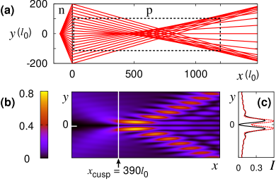
In Fig. 4(b), we plot near a cusp point , where the caustic curve of the classical trajectories is singular; see Fig. 4(a). We find that along the line of is zero, even at . For , the Klein effect of gives ; see Eq. (6). For , the intensity is determined by the interference of the three refracted waves Supplement propagating from the source to with incidence angles and , respectively, at the junction interface. In the limit of , the intensity is approximately given by , where is the dynamical phase of the refracted wave with incidence angle to the interface. In this case, , because of and the destructive interference coming from the Berry phase effect of ; for comparison, Fig. 4(c) shows the case where the Klein effect disappears. The result of is a clear manifestation of the Klein effect and the Berry phase . This result is contrary to the maximum intensity at the cusp point in the cases of a monolayer graphene junction CheianovLens and of geometrical optics with negative refractive index. We also discuss another way of detecting the Klein effect in an armchair nanoribbon in Ref. Supplement .
Conclusion.— We have studied the Klein effect in bilayer graphene. The effect can survive in the presence of energy band gap, and can be identified in a Veselago lens. We summarize our findings, by comparing the Klein effect in bilayer graphene and that in monolayer graphene. Both the effects result from Berry phase associated with pseudospin (but of different origin). The correspondence between them is found in the chirality ( for monolayer; for bilayer), the parameter space of the Berry phase (; ), symmetry (time reversal; in Eq. (5)), and destructive interference and phase jump (in reflection amplitude; in transmission) at normal incidence to the junction. Our findings will play an important role in graphene-based electron optics.
Note that, in experiments, it would be easier to study the Klein effect with a finite band gap than that of the zero-gap limit, since an (or ) junction can be realized by three (two) parallel gate electrodes, while the latter requires three (two) pairs of top and bottom gates.
This work is supported by NRF (2009-0078437).
References
- (1) M. I. Katsnelson, K. S. Novoselov, and A. K. Geim, Nature Phys. 2, 620 (2006).
- (2) A. H. Castro Neto et al., Rev. Mod. Phys. 81, 109 (2009). A. K. Geim, Rev. Mod. Phys. 81, 109 (2009).
- (3) C. W. J. Beenakker, Rev. Mod. Phys. 80, 1337 (2008).
- (4) V. V. Cheianov and V. I. Fal’ko, Phys. Rev. B 74, 041403(R) (2006).
- (5) T. Ando, T. Nakanishi, and R. Saito, J. Phys. Soc. Jpn. 67, 2857 (1998).
- (6) K. S. Novoselov et al., Nature 438, 197 (2005).
- (7) Y. Zhang et al., Nature 438, 201 (2005).
- (8) A. V. Shytov, M. S. Rudner, and L. S. Levitov, Phys. Rev. Lett. 101, 156804 (2008); A. Shytov et al., Sol. Stat. Comm. 149, 1087 (2009).
- (9) N. Stander, B. Huard, and D. Goldhaber-Gordon, Phys. Rev. Lett. 102, 026807 (2009).
- (10) R. V. Gorbachev et al., Nano Lett. 8, 1995 (2008).
- (11) A. F. Young and P. Kim, Nature Phys. 5, 222 (2009).
- (12) E. McCann and V. I. Fal’ko, Phys. Rev. Lett. 96, 086805 (2006); E. McCann, Phys. Rev. B 74, 161403(R) (2006).
- (13) T. Ohta et al., Science 313, 951 (2006).
- (14) E. V. Castro et al., Phys. Rev. Lett. 99, 216802 (2007).
- (15) J. B. Oostinga et al., Nature Mater. 7, 151 (2007).
- (16) Y. Zhang et al., Nature 459, 820 (2009).
- (17) R. Nandkishore and L. Levitov, arXiv:1101.0436 (2011).
- (18) K. S. Novoselov et al., Nature Phys. 2, 177 (2006).
- (19) V. G. Veselago, Sov. Phys. Usp. 10, 509 (1968).
- (20) V. V. Cheianov, V. I. Fal’ko, and B. L. Altshuler, Science 315, 1252 (2007).
- (21) H. Schomerus, Phys. Rev. B 82, 165409 (2010).
- (22) S. Park and H.-S. Sim, Phys. Rev. Lett. 103, 196802 (2009).
- (23) See supplemental material.
Appendix A Supplemental material for “ Klein Tunneling and Berry Phase in Bilayer Graphene with a Band Gap ”
In this material, we discuss the details (the calculation method and the properties) of the Veselago lens. We also discuss how to detect the Klein effect in a bilayer graphene nanoribbon.
Appendix B I. Electronic Veselago lens in bilayer graphene
In this section, we provide the method of calculating the properties of the Veselago lens, and also more information about the Veselago lens.
The wave intensity in the Veselago setup (a bilayer graphene junction) is obtained, using the plane-wave expansion method Cincotti . The setup is formed by the potential energy and band gap ,
The electron point source is located at in the region, where . The wave diverging from the source, , is described by the out-going wave of angular momentum zero,
Here, the upper (lower) sign corresponds to K (K′) valley, we used the cylindrical coordinate whose origin is at , , is the Hankel function of the first kind, is the wave vector of the wave, and is the normalization constant of the pseudospin part. The energy of the wave, related to by , is set to be as in the main text.
In the calculation of wave refraction, we apply the following approximation. In the spatial region where is satisfied, can be approximately written Cincotti in terms of plane waves,
where , , and . Here, can be regarded as the propagation angle of the plane wave in the region. The setup in Fig. 4 of the main text satisfies the condition of , hence the above approximation is well applicable to it; we have checked that the error due to the approximation does not alter the main features discussed in the main text. The approximation allows us to express the refracted waves in terms of the transmission coefficient through the junction, which is mentioned in Eq. (6) of the main text,
and , are defined in the same way as and , except for the subscript . The propagation angle of the refracted wave is governed by the conservation of , . We calculate by using the boundary matching method of plane waves at , and then obtain the wave intensity from . As we are considering the regime where the intervalley scattering is absent, the total intensity is the sum of and , i.e., there is no interference between the waves of K and K′ valleys.
Hereafter, we give additional information about the Veselago lens. We first mention the Klein effect in the smooth junction where and vary smoothly around . In the main text, for the sharp junction in which the values of and jump at , we find the feature that along the line of in the region of , when the condition of is achieved. This feature robustly appears in the smooth junction. The robustness comes from the facts that the symmetry in Eq. (5) of the main text is still valid, and that the value of is almost constant McCann_smooth when varies sufficiently smoothly.
Next we mention about electron propagation in the Veselago lens setup shown in Fig. 4 of the main text. In the region, the interference between three different refracted waves can appear at ; in contrast, there appears only a single refracted wave at . The three different waves propagate from the source to as follows. One of them propagates from the source to the junction interface with incident angle to the interface, and then it arrives at after its refraction at the interface. Here, the relation between and is found to be , where . Another wave follows the path with , which is the mirror-reflection (about axis) path of the wave with . The other wave follows the path with normal incidence of ; the transmission amplitude of this wave through the interface of is in fact zero, when the condition of for the Klein effect is achieved. The interference between the three waves shows the clear signature of the Klein effect and the Berry phase , as shown in the main text.
Appendix C II. Klein effect in armchair nanoribbon
In the main text, we find that the Klein effect and the Berry phase can be detected in the Veselago lens. In this section, we discuss another way of experimentally detecting the Klein effect in a bilayer graphene armchair nanoribbon.
The nanoribbon has armchair edges along axis and shows metallic behavior in the absence of external potential and band gap. Its stacking configuration is shown in Supplementary Figure 1(a). We consider an junction in the nanoribbon, formed by the potential energy and band gap ,
To see the signature of the Klein effect that the transmission probability of an electron through the junction is zero at normal incidence of , one needs to study the energy regime having only one transverse mode, which corresponds to the state with in the bulk limit Gonzalez . Focusing on this energy regime, we numerically calculate the transmission probability through the junction, by combining the tight-binding method and Green’s function Datta ; Sim2 ; as mentioned in the main text, is the transmission coefficient, and the energy of the incident electron is set by .
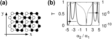
In Supplementary figure 1(b), we plot as a function of , where . We choose , , , , and the width of the ribbon , where is the lattice constant of graphene. Here, the subindex () refers to the region of and (). We choose and spatially varying over the length scale of around and ; in this case the intervalley mixing is prevented.
The transmission probability shows the perfect reflection of at . This shows the Klein effect, the transmission zero at normal incidence of in the bulk limit, hence, one can observe the Klein effect with tuning by gate voltages. This signature of the Klein effect (the perfect reflection) is distinguishable from the transmission valleys between resonance peaks. It is because the perfect reflection is independent of parameters such as , while the resonance peaks do depend on those parameters; is an electron wavelength in the region.
The Klein effect in the armchair nanoribbon is robust against the details of the shapes of and around the interfaces of the junction, provided that the valley mixing is negligible. The robustness implies that the Klein effect will survive in the presence of screened-Coulomb interaction, because the interaction may induce small change of the spatial shape of and at the interfaces Zhang .
The above finding appears in a metallic armchair ribbon with arbitrary width, provided that the energy regime has one transverse mode corresponding to the states with in the bulk limit. Note that it is difficult to observe the effect in ribbons with non-metallic armchair edges or with zigzag edges. This is because there is no state corresponding to the state injecting normal to the junction, i.e., because the band dispersion of the ribbon in the low-energy regime is different from that in bulk limit due to the edges.
The perfect reflection may disappear in the presence of valley-symmetry-breaking disorders, e.g., short range disorders and edge disorders. Such disorders induce valley mixing, and hence the Berry phase argument based on the time reversal and electron-hole symmetries defined in a single valley is not applicable.
References
- (1) G. Cincotti, F. Gori, M. Santarsiero, F. Frezza, F. Furno, and G. Schettini, Opt. Commun. 95, 192 (1993).
- (2) E. McCann, Phys. Rev. B 74, 161403(R) (2006).
- (3) J. W. Gonzalez, H. Santos, M. Pacheco, L. Chico, and L. Brey, Phys. Rev. B 81, 195406 (2010).
- (4) S. Datta, Electronic Transport in Mesoscopic Systems (Cambridge University Press, Cambridge, UK, 1995).
- (5) H.-S. Sim, C.-J. Park, and K. J. Chang, Phys. Rev. B 63, 073402 (2001).
- (6) L. M. Zhang and M. M. Fogler, Phys. Rev. Lett. 100, 116804 (2008).